

Abstract
Novel printed electronics are projected to grow and be manufactured in the future in large volumes. In many applications, printed electronics are envisaged as sustainable alternatives to conventional (PCB-based) electronics. One such application is in the semi-quantitative drug detection and point-of-care device called 'GREENSENSE' that uses paper-based printed electronics. This paper analyses the carbon footprint of GREENSENSE in order to identify and suggest means of mitigating disproportionately high environmental impacts, labeled 'sustainability hotspots', from materials and processes used during production which would be relevant in high-volume applications. Firstly, a life cycle model traces the flow of raw materials (such as paper, CNCs, and nanosilver) through the three 'umbrella' processes (circuit printing, component mounting, and biofunctionalization) manufacturing different electronic components (the substrate, conductive inks, energy sources, display, etc) that are further assembled into GREENSENSE. Based on the life cycle model, life cycle inventories are modeled that map out the network of material and energy flow throughout the production of GREENSENSE. Finally, from the environmental impact and sustainability hotspot analysis, both crystalline nanocellulose and nanosilver were found to create material hotspots and they should be replaced in favor of lower-impact materials. Process hotspots are created by manual, lab-, and pilot-scale processes with unoptimized material consumption, energy use, and waste generation; automated and industrial-scale manufacturing can mitigate such process hotspots.
Export citation and abstract BibTeX RIS

Original content from this work may be used under the terms of the Creative Commons Attribution 4.0 license. Any further distribution of this work must maintain attribution to the author(s) and the title of the work, journal citation and DOI.
Nomenclature
| Ag | Silver |
| Ag-ink | Nanosilver Ink |
| Al | Aluminium |
| AT | Austria |
| CNC | Cellulose Nanocrystals |
| CNF | Cellulose Nanofibers |
| CO2 | Carbon dioxide |
| DE | Germany |
| ECD | Electrochromic Display |
| EoL | End-of-Life |
| ES | Spain |
| FR | France |
| Gen 2 | Generation II Device |
| Gen 3 | Generation III Device |
| IL | Israel |
| IoT | Internet of Things |
| LCA | Life Cycle Assessment |
| LCI | Life Cycle Inventory |
| MA | Morphine antibody ink |
| MBGO | Methylene blue/graphene oxide Ink |
| MnO2 | Manganese dioxide |
| NFC | Near-field Communication |
| PCB | Printed Circuit Board |
| PET | Polyethylene terephthalate |
| polyNHS | Poly(N-isopropyl acrylamide-co-(N-methacryloxysuccinimide))ink |
| SE | Sweden |
| Supercap | Supercapacitor |
| TRIS Buffer | Buffered tris(hydroxymethyl)aminomethane (TRIS)-solution |
| WEEE | Waste Electrical and Electronic Equipment |
| Zn | Zinc |
1. Introduction
1.1. Background
With the advent of the IoT as a part of the 4th Industrial Revolution (Roselli et al 2015), the demand for smart devices in the fields of textiles, packaging, medical/health-monitoring, etc, is expected to boom (Kokare et al 2021). This growth in demand for smart devices is anticipated to be met by a new generation of 'printed electronics', rather than the conventional PCBs. Printed electronics enable the continuous manufacturing of flexible circuits in large volumes and at low costs for a variety of applications (Glogic et al 2021), and are therefore anticipated to spearhead the transition into a world of interconnected devices, sensors, and services (Wiklund et al 2021).
This new printed electronics technology is expected to enable 'electronics everywhere' (Hakola et al 2021), and their massive production volumes are expected to also give rise to environmental concerns, such as those associated with the creation and mismanagement of large volumes of WEEE (Glogic et al 2021, Nassajfar et al 2021). Despite these concerns, printed electronics are interesting for researchers and the industry because they seem to offer means to mitigate the foreseen environmental issues through the following manufacturing benefits (Wiklund et al 2021):
- Eco-design and resource efficiency.
- Minimization of energy use during production (and use-phase).
- Reduction in the use of hazardous substances.
- Possibility to use biodegradable materials.
1.2. GREENSENSE
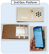
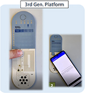
The project GREENSENSE (LEITAT 2018) envisages a point-of-care device for semi-quantitative drug detection in bio-fluids to tackle drug abuse in society. The GREENSENSE point-of-care solution is obtained by the integration of printed components, such as an ECD along with an energy storage unit (a battery or supercap), together with dedicated microchips on paper-based printed circuits. As a part of the project, specifically two different device (paper-based printed electronic) configurations were developed as shown in table 1: the Gen 2 configuration harvests energy from supercaps and solely relies on NFC connectivity for data transmission; the Gen 3 configuration visually presents the results on an ECD and utilizes a primary battery as the power source 10 .
Table 1. Comparison of Gen 2 and Gen 3 configurations of GREENSENSE.
| Gen 2 | Gen 3 | ||
|---|---|---|---|
Components:
|
|
|
Components:
|
| Use: Unpacking the sensor activates the supercapacitor and powers up the device; the saliva sample may then be placed on the biosensor for drug detection; the data about drug detection will be transferred to an app on the mobile phone using the NFC antenna. | Use: Once turned on using the printed buttons, the device draws power from the battery; the saliva sample can be tested using the biosensor; the results of the drug detection may be read directly on the ECD of the device or be transferred to a mobile app using the NFC antenna. | ||
Various synthetic and biological materials (Yang et al 2011, Li et al 2020) may be employed in the substrate of printed electronics; however, paper was selected for GREENSENSE as it has the advantage of being a flexible, cheaply available, and biodegradable material with low environmental impacts and an established recycling system (Hakola et al 2021). Due to its surface roughness and porosity, the paper is coated with a film of CNCs to facilitate the printing of circuit layout using conductive Ag-ink (Fernandes et al 2020). The overall goal of GREENSENSE is to prepare a paper-based, low-impact, and functional printed electronic system that benefits society without posing major environmental harm in the face of improper disposal or leakage to nature.
1.3. An early-stage sustainability assessment
The components (e.g. energy storage units, ECD, etc) and processes (e.g. circuit printing, components assembling, etc) utilized in the GREENSENSE point-of-care device are still in their infancy and consequently not optimized for large-scale production or supply to the market. For such an early-stage technology, a sustainability assessment is pivotal and can prove to be a powerful tool to weed out potential environmental problems already during the development phase. According to literature, the materials selected and the processes applied for manufacturing or integrating components at the early stages of development contribute to the majority of the environmental impacts in any finalized product (Kunnari et al 2009). Consequently, a sustainability assessment conducted at the early-design phase is necessary to actively steer the development process toward more sustainable products by recommending materials, designs and processes with lower environmental footprints (EFs). On the other hand, using a sustainability assessment to balance functionality and sustainability for mature technologies (with optimized and rigid processes and supply chains) may not be as fruitful: the recommendations from a sustainability assessment may be viewed by the product developers as unrealistic and challenging to adopt (lock-in effect).
A LCA is the best tool to assess the environmental impacts from existing as well as novel materials, processes, and technologies (Glogic et al 2021). By comprehensively analyzing the material consumption, energy requirements, and waste generation throughout the respective lifecycles of materials, processes, and products, LCAs serve as decision support tools that aid in sustainable material selection, product eco-design, sustainable disposal and EoL, and policy development to minimize environmental impacts (Liu et al 2014).
Although there are LCA studies in literature focusing on the environmental impacts of printed and flexible electronics (Kanth et al 2012, Liu et al 2014, Wan et al 2015, 2017, Välimäki et al 2020, Glogic et al 2021, Hakola et al 2021, Kokare et al 2021, Nassajfar et al 2021), LCA results have not yet been consolidated into a framework to support the future development of sustainable printed electronics. The research presented here is an LCA of the GREENSENSE manufacturing and integration chain that aims to offer guidance on the development of sustainable printed electronics. By limiting the LCA's scope to the production phase and additionally conducting a hotspot analysis, the largest sources of environmental impacts during the manufacturing of GREENSENSE have been highlighted, broken down into explicit shares, and attributed to the respective materials and components.
Focussing on prototyping, production, and design phases in LCAs allows for the selection of sustainable materials, eco-design, and finally results in environmentally friendlier products (Manjunatheshwara and Vinodh 2021). The use phase and the EoL are also relevant in an LCA; however, product developers have limited control over these stages of the life cycle. The use phase is dependent on the user of the product and the EoL is largely determined by the waste management system. In contrast, the materials and processes used during the production phase are at the discretion of the product developer and they can be optimized to minimize environmental impacts. Another reason for focusing on the production phase is that GREENSENSE, like many prospective printed electronics applications, is anticipated to be manufactured in large volumes as it is a single-use and disposable point-of-care device with a short lifespan (Keskinen 2012). The large quantities of waste envisioned from such a readily disposable device are likely to be ineffectively managed by the current electronic waste management system; i.e. despite all favorable attempts for recycling, there is a possibility that these devices and the valuable materials contained in them will end up in the environment or landfills (Hakola et al 2021). As a result, the design of the GREENSENSE device is reliant on compostable biomaterials, such as paper, so mismanagement at the EoL and the leakage to nature or landfilling causes minimum environmental impact. Apart from the release of toxic substances and the persistence of waste in nature, not undertaking the recycling of electronics leads to the loss of valuable materials and critical resources to the environment (Li et al 2020). Thus, the sustainability hotspot assessment of the production processes can be crucial in quantifying, justifying, and also minimizing the exact impacts created by materials that, by design (for composting), are intended to be lost to nature. For a device designed for composting, the materials used should not only fit the criteria of being biodegradable and biocompatible but also have low sourcing impacts. The best design for compostable electronics would include utilizing minimal quantities of non-critical and non-precious functional materials so that their loss to nature does not create resource efficiency concerns. Thus, the objective of this sustainability assessment is to identify the critical materials and design considerations, underscore the major sustainability roadblocks for GREENSENSE, and finally produce recommendations that inform eco-design principles relevant to the entire printed electronics sector.
2. METHODS
2.1. Production model for GREENSENSE
The production of GREENSENSE is a collaborative effort within a consortium consisting of research institutes and companies spread across different countries (LEITAT 2018). Each consortium member undertook the development of materials and manufacturing of components that were finally assembled into the GREENSENSE devices. Figure 1 illustrates the entire GREENSENSE production chain consisting of lab-, pilot-, and industrial-scale processes. In-depth details about the production of individual components are available in chapter S7 of the supplementary material. Additionally, figure 1 also denotes processes that occur at an industrial scale; processes not classified as industrial utilize a mix of pilot- and lab-scale equipment and thus cannot be further classified categorically as either lab or pilot scale. Hence, all non-industrial processes in figure 1 lie within the lab- to pilot-scale spectrum.
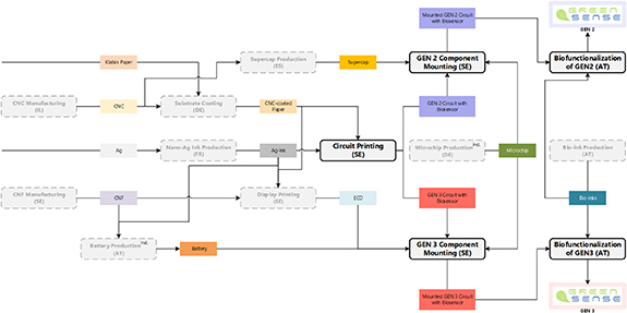
Figure 1. Process diagram illustrating the materials, components, and processes utilized for manufacturing the Gen 2 and Gen 3 configurations of GREENSENSE; the country or the geographical region of the respective processes have been listed below the process name in the round '()' brackets as abbreviations; superscript 'ind.' indicates an industrial-scale process, otherwise, the process is somewhere in the spectrum ranging from lab- to pilot-scale; the three umbrella processes: circuit printing, component mounting, and biofunctionalization have also been highlighted.
Download figure:
Standard image High-resolution imageThe process model in figure 1 depicts the production of the Gen 2 and Gen 3 architectures of the GREENSENSE device. As expressed in table 1, Gen 2 and Gen 3 differ in terms of functionality: Gen 2 is a compact system, that relays on NFC communication that uses 2-supercaps as an energy source, whereas Gen 3 integrates an ECD to provide a readout of the results and utilizes a battery as an energy source. The added functionality of Gen 3 makes the device larger, and more complex and differentiates its production processes (e.g. assembling a larger number of components) from those of Gen 2.
The complex production model in figure 1 has been further simplified here by underscoring three 'umbrella processes': circuit printing, component mounting, and biofunctionalization. Each of the materials used, processes applied, and components developed for GREENSENSE can be classified into a corresponding umbrella process. In the correct sequence, the following umbrella processes encapsulate the entire production model of GREENSENSE.
2.1.1. Circuit printing
The first umbrella process is circuit printing. This includes the sourcing and functionalization of the substrate and monolithic printing (via flatbed screen printing technology) of the circuit, electrodes for the biosensor, and an NFC antenna. The substrate used in the case of the GREENSENSE device is paper (Hakola et al 2021) that has been coated with a 2–4 µm film of CNCs (Börjesson and Westman 2015, Sharma et al 2020). On this prepared substrate, the circuit, antenna, and sensor electrodes were printed using an Ag-ink (Fernandes et al 2020) in combination with a variety of commercially available carbon, Ag/AgCl, and dielectric inks. The outcomes of circuit printing are the two printed electronic circuits on which components are mounted to prepare the Gen 2 and Gen 3 biosensing platforms respectively.
2.1.2. Component mounting
Once the printed circuit is ready, the electronic components are mounted using a Ag-based conductive adhesive in this second umbrella process. Gen 2 and Gen 3 share the rigid components (the microchip and two capacitors) which are mounted using an automated process developed by adapting tools and processes commonly used in the assembly of standard PCBs. Apart from the rigid components, the Gen 2 device incorporates two-supercaps for energy storage whereas Gen 3 incorporates a primary battery. Furthermore, Gen 3 has an ECD to display the results. The mounting of the supercaps, the primary battery, and the ECD is performed manually.
2.1.3. Biofunctionalization
This final umbrella process is biofunctionalization (Petersen 2017) and it involves the activation of the sensor electrodes using specifically formulated bioinks (Jose et al 2016). The nature of the biofunctionalization dictates the performances of the biosensor (e.g. selectivity, detected analyte, and sensitivity); the GREENSENSE platform has been biofunctionalized to detect morphine in saliva.
2.2. LCA
LCAs are effective tools to understand the environmental impacts of existing as well as novel technologies (Glogic et al 2021). In literature (Schmidt and Pizzol 2014, Zheng et al 2018), the LCA methodology as per ISO 14040 has been explained in great detail and specifically applied for both, conventional as well as novel printed electronics. The following steps explain the LCA methodology applied in this study.
2.2.1. Goal and scope definition
A production or a cradle-to-gate LCA (Zheng et al 2018) was conducted for the system described in figure 1. The functional unit for the assessment was determined to be a single unit of the Gen 2 and Gen 3 devices produced. As mentioned previously and explained in table 1, the functionality of a single unit of Gen 2 and Gen 3 differs: Gen 3 has an additional display (ECD) to read out the results from the biosensor's drug detection. This difference in functionality implies that a comparison between the two configurations is moot from the LCA perspective due to the absence of functional equivalence (Kim et al 2017). That being said, the goal of this study is not to compare the impacts of the two configurations, but rather to identify the sustainability hotspots in their production chains and bust sustainability myths for material scientists and developers of printed electronics.
2.2.2. Modeling the LCI
The first step in modeling the LCIs was to collect the data from all the consortium partners on their specific processes: quantities related to material inputs, material composition, energy requirements, waste production, and any other emissions were obtained through technical process surveys. The information from the surveys was further modeled into LCIs using the background data from v3.7.1 of the Ecoinvent database (Wernet et al 2016). The LCIs are comprised of datasets on individual materials, components, and processes. The energy consumption in each dataset is regionalized and modeled based on the respective energy mixes of the processes' country or geographical region abbreviated in figure 1. Nevertheless, certain specific activities have been excluded from LCI modeling, particularly those related to transportation and infrastructure. Since the manufacturing of the GREENSENSE devices is limited to lab and pilot scale, the transportation of materials and components between facilities was carried out by using parcel delivery services that handle small-volume packages. Since such a transportation model is neither representative of a real supply chain nor traceable, it was excluded from the LCI modeling. Additionally, setting up of infrastructure (such as the construction of research facilities or manufacturing of equipment) utilized during GREENSENSE is also beyond the scope of the modeled inventory; this is primarily because the same equipment and facilities are involved in multiple research projects and attributing shares to a single project was not possible. Notwithstanding, energy consumption for rooms and operation of equipment for manufacturing GREENSESNE is modeled in the LCIs as it was possible to measure and report in the initial data survey on the processes.
2.2.3. Impact assessment
Finally, the impact assessment was carried out as per the ILCD's 2018 method (Fazio et al 2018) within the activity-browser (Steubing et al 2020) framework of Brightway2 (Mutel 2017). Furthermore, the climate change impacts (carbon footprints) were calculated and have been presented in kilograms of CO2 equivalents (kg CO2 eq.). As mentioned earlier, comparing the results from the impact assessment of both configurations is not sensible because of the differing functionalities. However, it is also true that the carbon footprints of Gen 2 and Gen 3 have limited interpretability individually and require contextualization. Therefore, solely for the purpose of contextualizing (and not comparing) the results of the impact assessment, the carbon footprints of both configurations have been juxtaposed further on.
2.3. Sustainability hotspot analysis
The results from the impact assessment are the carbon footprints of the materials, components, and processes used during production. A further step is to identify the climate change hotspots in the production process by tracing the impacts back to the respective materials used, energy consumed, waste generated, and emissions. This is achieved by mapping the 'flow of impacts' across the processes and materials during production. The impact flow has been represented with a Sankey diagram plotted using the ipython Sankey widget (Lupton and Allwood 2017).
With the help of the Sankey diagram, key hotspots have been identified and classified as:
- Materials hotspots from materials with a disproportionately high impact considering their used quantity.
- Process hotspots from unoptimized processes that use excessive quantities of materials and energy and generate excessive quantities of waste.
3. Results
3.1. Impacts from individual components and processes
The climate change impacts from the processes and the components used in the manufacturing of the Gen 2 and Gen 3 devices are illustrated in figure 2. These impacts have been classified into the respective umbrella processes, i.e. circuit printing, component mounting, and biofunctionalization. Finally, the total climate change impacts from the production of the GREENSENSE devices have been calculated by adding up all the impacts from the umbrella processes. Furthermore, the climate change impacts from the production of GREENSENSE have been contextualized by juxtaposing the results for Gen2 and Gen 3; these impacts can be further compared to impacts from common items and products (see table S1).

Figure 2. The total climate change impacts for the manufacturing of Gen 2 and Gen 3 GREENSENSE devices obtained by adding up the impacts from specific materials, components, and processes in the respective umbrella processes: circuit printing, component mounting, and biofunctionalization; superscript 'ind.' indicates an industrial-scale process, otherwise, the process is somewhere in the spectrum ranging from lab- to pilot-scale.
Download figure:
Standard image High-resolution imageFigure 2 shows that the total carbon footprint of the Gen 3 (3.269 kg CO2 eq.) device exceeds that of Gen 2 (1.354 kg CO2 eq.). The larger size of the Gen 3 device entails higher material usage (e.g. substrate and Ag-ink for circuit). Moreover, the presence of an additional and heterogeneously mounted ECD on the Gen 3 circuit, has an additional impact (0.424 kg CO2 eq.) that is associated with the component in itself and with the process and materials used for its mounting. The larger size of the Gen 3 device also means that it requires a substrate with a larger area and consequently, the substrate impacts in Gen 3 are higher than that of Gen 2. Finally, the larger size of the Gen 3 device also influences the efficiency of the biofunctionalization process since the larger Gen 3 devices can only be functionalized individually, whereas multiple Gen 2 devices could be simultaneously functionalized in a batch. Therefore, for the same amount of energy required for biofunctionalizing each Gen 3 sensor, up to four Gen 2 sensors can be biofunctionalized and this is reflected in the higher biofunctionalization impact of the former (0.484 kg CO2 eq. for biofunctionalizing Gen 3 versus 0.148 kg CO2 eq. biofunctionalizing for Gen 2). Essentially, the cost of higher functionality of Gen 3 is its higher carbon footprint in the LCA.
The power source is the only component for which the impacts of Gen 2 exceed that of Gen 3. Due to the voltage requirement of the microchip (>3.5 V), its operation is made feasible by the use of several energy storage units that are connected in series. The Gen 2 device requires two supercaps to operate while the Gen 3 device uses a single energy unit consisting of three monolithically-integrated batteries. When it comes to the impacts due to the energy sources, the manufacturing of a single battery unit (0.152 kg CO2 eq.) is comparable to those of a single supercap (0.142 kg CO2 eq.). Despite having a lower energy density than the battery unit, supercaps have a high impact because they are produced to a great extent manually at the lab scale in contrast to the semi-automated and industrial-scale manufacturing of the battery units.
Apart from the battery, the microchip is also manufactured at an industrial scale. The negligible impacts from the microchip (0.008 kg CO2 eq.) in figure 2 exemplify the inherent environmental advantage of optimized industrial-scale processes: the impacts from the battery and the microchip are minute in comparison to the impacts from the other components manufactured at a lab or pilot scale.
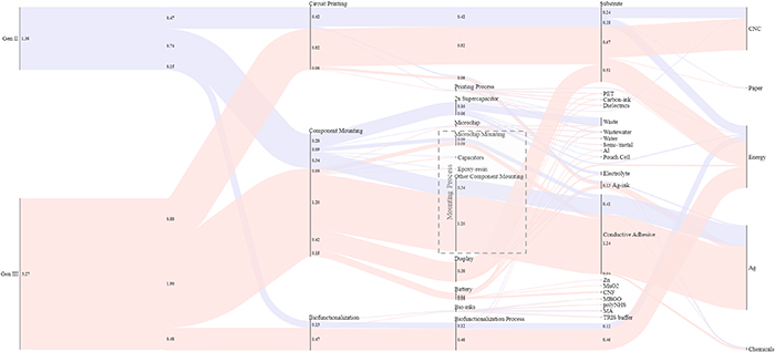
3.2. Impact contributions and sustainability hotspots
The Sankey diagram in figure 3 further dissects the climate change impacts depicted in figure 2 based on the information in the supplementary material. The overall carbon footprints of the Gen 2 and Gen 3 devices are illustrated on the left side of the Sankey diagram, while the flow of the climate change impacts (referred to further as just 'impacts') is traced across each umbrella process (i.e. the circuit printing, component mounting, and biofunctionalization), and listed towards the middle-left of the Sankey diagram. The footprints are further traced to the components and processes (from figure 2) in the middle of the Sankey diagram. Finally, all the impacts can be eventually traced and attributed to the materials and energy required during production, and they are shown in the middle- and far-right of the Sankey diagram.
Figure 3. Contribution to the total climate change impacts (in kg CO2 eq.) of the Gen 2 (lilac) and Gen 3 (rose) GREENSENSE configurations on the left; the flow of impacts is traced across each umbrella process (i.e. the circuit printing, component mounting, and biofunctionalization) listed towards the middle-left of the Sankey diagram; the impacts are further traced to the components and processes in the middle of the Sankey diagram; finally, all the impacts are eventually traced and attributed to materials and energy required during production and shown towards the middle-right and far-right of the Sankey diagram; the 'other component mounting' represents the impacts from the manual mounting of the display and energy sources which is a manual process and thus distinguished from the automated mounting of the microchip represented by 'microchip mounting'.
Download figure:
Standard image High-resolution image
As depicted in figure 2 and the right area of figure 3, a large share of impacts from both Gen 2 and Gen 3 manufacturing arise from the substrate. Within the substrate, the paper has a minority share in the impacts of around 1% despite being the essential material for the substrate and having a mass share of 99% (see figure S1). Whereas, the CNC, despite having a dry mass share of just ca. 1%, contributes over 56% of the impacts in the substrate. The remaining 43% of the impacts in the substrate are ascribed to the energy required for the pilot-scale coating of the paper with CNC. This impact profile of the substrate is also crucial for the ECD that is printed, as a stand-alone component, on the same substrate material and subsequently integrated into the Gen 3 circuit.
The waste generated during production processes requires treatment, and this is found to be a substantial source of impact specifically for the production of supercaps and other lab-scale processes. Most of these lab-scale processes also have a high impact due to unoptimized energy consumption. Biofunctionalization is one such lab-scale process that is conducted in batches, and the largest share of its impacts arise from the energy requirements for the process rather than the bioinks actually used for biofunctionalization.
The Ag, present in the Ag-ink and the conductive adhesive, is a precious metal that has a high sourcing impact. Thus, Ag is by far the biggest sustainability hotspot in the production of GREENSENSE as it is the largest sole contributor to the total impacts of Gen 2 and Gen 3. Interestingly, as seen in figures 2–3, the impact from the Ag-ink itself is relatively small compared to the conductive adhesive and the substrate. This highlights the benefits of additive manufacturing for smaller circuits with small conductive areas as only adding on the required amount of materials through the efficient printing process proves to be eco-friendly. A much larger impact may be attributed to the conductive adhesive used to integrate the microchip and 'other components' (to represent the mounting of the display and power source in figure 3) on the circuit. The reason for distinguishing the mounting of the microchip from that of the 'other components' in figure 3 is the automated nature of the former. The machine-based mounting process of the microchip uses a minimal and optimized amount of conductive adhesive. All the 'other components' are mounted by hand, which inadvertently leads to an unoptimized and excessive use of the Ag-based conductive adhesive, and consequently, a higher impact from the mounting process.
4. Discussions
4.1. Key hotspots
The results underscore material and process hotspots in the production chain with disproportionately high impacts. These impacts may arise as a result of the following reasons: use of materials with high environmental impacts (environmentally intensive materials); unoptimized processes and design inefficiencies leading to excess material and energy usage or waste production.
4.1.1. Material hotspots
Material hotspots are created by environmentally intensive materials when they are used in small quantities. This is observed in the case of CNC used as a coating for the paper substrate. Counterintuitively, CNC is one of the environmental hotspots in the production of Gen 2 and Gen 3 despite being benign and a renewable material originating from abundant biomass. It is the high energy requirement for the manufacturing of the nanomaterial, that makes this material a hotspot, particularly from a global warming perspective (Gao et al 2018). In our assessment, 98% of the impacts from CNC originate from the high energy demand required for isolating and producing the nanomaterial; therefore replacing the feedstock (pulp from virgin wood) to waste biomass or agricultural residues will have a limited sustainability benefit (Tao et al 2017). This raises a larger argument about how bio-based materials are always perceived as 'green' alternatives to fossil materials, which is not always true in reality. There are of course established bio-materials with a low impact such as paper; however, there is a growing interest in the printed electronics community to use novel biopolymers (Nassajfar et al 2021) with a 'green' reputation that may not hold (Ivanović et al 2021).
Another key material hotspot in the production process of GREENSENSE is Ag, which is even more environmentally intensive to procure than CNC. From a global warming perspective, the procurement of 1 kg of Ag has a climate change impact of ca. 458 kg CO2 eq., which is ca. 72-times higher than that of 1 kg copper (Wernet et al 2016) that is used in conventional PCB-based electronics solutions. Ag is a precious and difficult-to-mine metal that consequently is environmentally intensive to procure. The high impact of Ag in conductive inks is a widely-known issue in the printed electronics community (Välimäki et al 2020, Nassajfar et al 2021). Despite several efforts to develop alternative conductive inks based on copper, Zn, and carbon with lower environmental impacts (Glogic et al 2021, Majee et al 2021, Wiklund et al 2021), the printed electronic sector still heavily relies on the use of Ag because of its easy processability, electrical performances, and stability.
A new learning from the present study is the large impact of component mounting due to the use of Ag-based conductive adhesives. In fact, the Ag from the conductive adhesive contributes the largest share of impacts in the production of GREENSENSE. This is interesting because while the Ag-ink has a significant impact, it is dwarfed completely by the impacts of the conductive inks. At the time of the present study, no further research was found on the development of conductive adhesives using alternative metals with lower environmental impact. Since many complex components are difficult to print directly or integrate monolithically on the substrate, the demand for component mounting may rise with the growth in applications for printed electronics. Hence, the exploration of more sustainable mounting adhesives or processes (e.g. low-temperature soldering) would be viable and could significantly aid in reducing the impacts from printed electronics. Changing the materials used for the mounting process would be an obvious approach to reduce its impact; however, a less obvious but equally relevant approach would be to optimize the design of the device to facilitate the monolithic integration of components.
4.1.2. Process hotspots
Apart from the materials, unoptimized processes also create sustainability hotspots in the production chain. Particularly lab-scale production processes result in higher impacts as a consequence of the unoptimized material and energy consumption. In comparison, large-scale production processes benefit from enhanced efficiency, optimized material use, and energy consumption, along with minimized waste generation as a result of scaling up a process (Piccinno et al 2016). Additionally, some lab-scale processes are very energy demanding because material development occurs in clean rooms, which draw a lot of power (Kunnari et al 2009). Thus, in the present study, it is seen that industrial processes simply outclass laboratory processes in terms of impacts; this was also anticipated at the data collection phase when the process surveys from labs highlighted the large amounts of energy required, materials used, and waste generated per unit quantity of the output. The majority of the energy hotspots are created by the substrate coating process and biofunctionalization, neither of which is an industrial-scale process (details in chapter S7). Moreover, the treatment of waste is also seen to create significant impacts in the lab-scale manufacturing of supercaps.
Another underlying reason for process hotspots may be design limitations. Certain processes may be automated and optimized even at a lab scale; moreover, devising a product design that is ideal for automated processes is challenging and tedious (Bonnassieux et al 2021). For example, the biofunctionalization process is automated but performed with a lab-scale device that only allows conducting this step in batches. Furthermore, the area that the machine can biofunctionalize in one go is constrained; thus, the larger size of Gen 3 implies that only a single platform can be biofunctionalized in a batch, and consequently, the energy impact for biofunctionalization per Gen 3 device rises. Similarly, the lab-scale mounting of the microchip is achieved with an automated machine that minimizes the use of the high-impact conductive adhesive. However, not all components are designed to be mounted by machines, and these components have to be mounted on the circuit manually.
A clear example of how the system design can affect its overall impact can be deduced by semi-empirically comparing the overall impacts of Gen 3 when the ECD is monolithically integrated within the circuit substrate. The monolithic integration of the ECD on the circuit substrate will avoid the need for additional substrate (that accounts for ca. 80% of the overall ECD impact) and will remove the need for the use of Ag adhesive for its assembling (ca. 60% of the overall adhesive usage in Gen 3). Thus, this change in the system can be expected to reduce the overall impact of Gen 3 by ca. 40%. It must be noted that this semi-empirical evaluation does not account for other factors that might come into play due to the monolithic integration of ECD such as a higher system complexity that might affect production, yield, and subsequently increase waste production.
Hence, the high impacts of the mounting of components may be attributed to the high impacts from the Ag-based conductive adhesives and the design of components that cannot be mounted by automated machinery. Both of these lead to the creation of process hotspots during 'other component' mounting.
4.2. Limitations
Data availability is always restricted to some extent in LCA studies. In general, there is a dearth of data to model the LCIs for proprietary commercial formulations, especially for novel developments (Kunnari et al 2009). Past LCAs (Wan et al 2017) had access to no data for certain components of printed electronics and relied extensively on assumptions for their evaluation. For the present research, being a part of a consortium allowed access to much of the proprietary data that would not have been available otherwise. Nevertheless, it was not possible to obtain all the needed data for certain commercial inks, specifically carbon and dielectric inks. Those datasets have been created by adopting relevant proxies that pre-existed in the Ecoinvent database or modeled based on literature and assumptions. The said assumptions and proxies, however, were deemed to be reasonable given that their impact shares are unlikely to be comparable to CNC and Ag and drastically alter the final outcomes of this research.
Another limitation arises from the direct comparison of results based on lab- and industrial-scale data. As mentioned earlier, lab-scale processes are unoptimized and the data from such processes cannot capture the environmental benefits observed in industrial- and mass-scale production. This was highlighted by the negligible impacts from the industrial manufacturing of microchips in comparison to the other processes in the assessment. Although there are methods in literature (Piccinno et al 2016) to scale up lab processes and model impacts from industrial-scale production, the data required to build and the relevant scaled-up process models were unavailable. Nevertheless, the comparison between impacts from different scale processes is still relevant and valid as lab-scale results can still provide some insights into possible impacts from their scaled-up counterparts. Furthermore, the lab- or pilot-scale data and the higher corresponding impacts are representative of current reality and state-of-art. Projecting and presenting lower industrial-scale impacts (with uncertainty) using non-standardized upscaling methods (Shibasaki et al 2007, Piccinno et al 2016) may present an overly optimistic picture (unless verified through actual scaled-up manufacturing of printed electronics in reality) that may be misused for marketing purposes. Since completed industrial manufacturing of printed electronics is presently not widespread, data for modeling upscaling is unavailable, and attempts in this direction will possess limited scientific merit (Cucurachi et al 2018, Maranghi et al 2020).
Finally, the scope of the present assessment is limited to the carbon footprint from the production process. Other environmental impact categories, such as ecotoxicity, water footprint, etc have been excluded from this assessment as it was considered improbable that they would provide more information on or underscore different hotspots (Esnouf et al 2019). Nevertheless, there is a risk of 'burden-shifting' and negligence toward other environmental impacts by solely focusing on carbon footprints (Algunaibet and Guillén-Gosálbez 2019, Jackson and Brander 2019) or having a 'carbon-tunnel vision' (Jensen 2021). A possible solution could be to consider the EF 3.0 (European Commission 2021) or the ReCiPe 2016 (Huijbregts et al 2017) methods for impact assessment that can simultaneously compute and aggregate impacts over multiple categories but the final aggregated environmental scores obtained often lack physical meanings (Kalbar et al 2017). For the printed electronics sector, particularly organic and bio-based electronics, more research is required to understand which environmental impact categories are pertinent to specific applications in order to minimize environmental burden shifting (Johnsen and Løkke 2013). However, the product environmental footprint (PEF) category rules for IT equipment (European Commission 2018) identify total climate change, resource use (minerals and metals), resource use (fossils), and particulate matter/respiratory inorganics emissions as the most relevant impact categories for conventional electronics and PCBs; these impact categories would be particularly relevant and could be applied in studies that aim to benchmark the impacts from printed electronics against conventional electronics.
There are other production concerns related to printed electronics considered to be beyond the scope of this assessment, such as occupational health and safety risks from the fumes emitted during the handling and curing of inks in the printing process (Kunnari et al 2009, Keskinen 2012). These issues related to inks could be mitigated by using water or sustainable solvent in the ink media (Yang et al 2011, Larsen et al 2021), but quantifying the benefits of the same to the occupation health and safety of workers would not be possible within the scope of an LCA. Additionally, apart from the high impact related to Ag, there are various eco-toxicological concerns associated with the release of nano-Ag (Keskinen 2012, Wiklund et al 2021) into the environment particularly from compostable printed electronics. However, these are concerns more relevant in EoL studies in which the leakage of nano-Ag to the environment from single-use and compostable printed electronics would be the prime focus. Nevertheless, all the externalities (Moreau et al 2021) mentioned above are expected to have a bearing on the sustainability of the GREENSENSE device and we hope to further explore them in future research. Finally, as stated earlier, this assessment excludes the EoL and focuses on the production phase because the product designers and material scientists can tweak the latter's efficiency and sustainability but have limited control over the former. Regardless, assessing the EoL and understanding the best waste treatment options are also pertinent to developing sustainable printed electronics. For readers interested in the EoL of printed electronics, we recommend our other study (Sudheshwar et al 2023) which looks at the topic in detail and highlights the importance of circular economy criteria (Hummen and Sudheshwar 2023) and recycling in the lifecycle of paper-based printed electronic systems like GREENSENSE.
5. Recommendations
The intention behind the use and development of printed electronics that utilize biodegradable substrates (such as paper) is to minimize environmental impacts in the case of mismanagement at the EoL. However, such an approach does not focus on the recycling of materials and may simply cause the leakage of precious resources, with high sourcing impacts, to the environment. Thus, it is necessary to focus on the production of such electronics and mitigate the key material and process hotpots from the perspective of sustainability. A production LCA can serve as a guiding tool in the selection of lower-impact materials at the development stage and ensure safe and sustainable eco-design for early-stage technologies.
The LCA presented in this assessment focuses on the production of GREENSENSE and it highlights the heavy dependence of printed electronics on Ag, which is a material with high sourcing impacts and is used in conductive inks and adhesives. Thus, there is a need for the printed electronics sector to explore conductive inks and adhesives for additive manufacturing based on metals with lower environmental impacts. Another material hotspot in the assessment was CNC, which was surprising, as it is a biomaterial; thus, it is important to reassess the general perception about biomaterials being that they always have low environmental impacts and are 'green' to procure.
Finally, the hotspot analysis highlights the discrepancy in the impacts arising due to the scale of a process: smaller unoptimized processes at a lab scale have higher impacts because per quantity of output, they have high energy and material consumption/usage along with more waste and emissions. Thus, industrial processes outclass lab- or pilot-scale processes in terms of environmental impacts. Additionally, when possible, monolithic integration should be adopted for the circuit components in additive manufacturing of printed electronics as it leads to the use of lower material quantities. Finally, novel component designs, processes, and tools (machines) should be developed to minimize manual steps in the manufacturing of components and systems for printed electronics.
Data availability statement
The data generated and/or analyzed during the current study are not publicly available for legal/ethical reasons but are available from the corresponding author on reasonable request.
Funding
This project has received funding from the European Union's Horizon 2020 research and innovation program under Grant Agreement No. 761000 GREENSENSE.
Footnotes
- 10
GREENSENSE generation I platform utilized a conventional PCB system and has thus been excluded from this assessment.
Supplementary data (0.5 MB PDF)