


Abstract
Nanocomposites formed by silver nanowires (AgNWs) embedded in a polymer matrix are a convenient way to deposit thin films with electrical conductance and high transparency on different substrates. Nanocomposite resists containing AgNWs in a poly(methyl methacrylate) solution can be effectively used to produce conductive coatings in a straightforward manner. Here, we show that by adding a sacrificial layer of polyvinylpyrrolidone on a glass substrate, prior to the nanocomposite resist, it is possible to obtain large-area free-standing films of about 450 nm with electrical conductance and high transparency. The films can be transferred to different surfaces and materials including non-flat substrates. The formation of conductive stacks by piling two layers was also demonstrated. The optical, electrical, and structural properties of these free-standing films were studied obtaining films with transmittance T(%) = 78% at 550 nm, sheet resistance Rs = (670 ± 40) Ω sq−1 and surface roughness Ra = (50 ± 10) nm. We studied the strain resistance behavior of films transferred to polyethylene terephthalate sheets under bending tests finding a sensitivity of (0.51 ± 0.01) Ω deg−1 and a gradual increase in the resistance during cycling. In addition, thin flexible supports can be added by covering the nanocomposite film with polydimethylsiloxane (PDMS) prior to its release, enhancing the mechanical robustness and improving the manipulation of the films.
Export citation and abstract BibTeX RIS
1. Introduction
Transparent and flexible conductive films are essential elements of many developing technologies. They are part of sensor devices, solar panels, antennas, electromagnetic shielding, electrodes and many more. In particular, the current technological trend aims at achieving coatings with high electrical conductivity, high transmittance in the visible spectrum, good adhesion to flexible substrates and adequate mechanical properties. Among the different strategies to achieve electrical conductivity, the use of silver nanowires (AgNWs) as filler material within a matrix, usually polymeric, stands out as shown by recent reviews [1, 2]. The electrical percolation obtained at low metal phase concentration is favored by the high aspect ratio of AgNWs. In addition to percolation, the inclusion of AgNWs in a nanocomposite constitutes a mechanical reinforcement [3]. It is thanks to this that under certain conditions conductive nanocomposites can operate without the need for a supporting substrate, thus transitioning from being coatings to become self-supporting films.
Self-supported thin films possess intrinsic properties of interest due to their low dimensionality and low mass. In addition, their ability to be transferred to non-flat surfaces makes them especially useful for building 3D electrical architectures. They are of particular interest for the fabrication of microresonators, microelectromechanical systems (MEMs) [4, 5], supercapacitors [6], membranes, artificial skins [7], biosensors [8] and more.
Precedents of free-standing conductive films were developed in the last decades making use of electronic properties of graphene oxide [9], carbon nanotubes [10], and conductive polymers [5, 11]. Free-standing conductive films containing AgNWs were previously studied by several groups. In 2015 a peeled-off nanocomposite film formed by AgNWs and the photopolymer NOA63 was reported for the fabrication of flexible organic light-emitting devices [12]. Films containing AgNWs and graphene oxide transferred to poly(methyl methacrylate) (PMMA) films, 25 µm thick, were reported by Bang et al [13]. In 2018, a polyimide-AgNWs thin film was reported as a self-supported conductive film with low surface roughness, a sheet resistance of 7–13 Ω sq−1 and optical transmittance surpassing 90% [14]. The films were shown to possess high thermal and mechanical stability as a self-supported film but could not be transferred to other surfaces or deposited over a 3D structure. Most recently, 3 µm thick films of AgNWs deposited on a Ni mesh standard out as an interesting alternative for electromagnetic shielding [15]. Transparent and conductive films based on AgNWs-polydimethylsiloxane (PDMS) layers were reported with interesting folding properties [16].
In previous works, we showed that nanocomposites based on AgNWs dispersed in PMMA resists were suitable for building transparent heaters [17] and for the microfabrication of microstructures either by soft-lithography techniques or by direct electron beam lithography [18]. Here, via a two-step spinning process, we report on the straightforward method for the fabrication and transferring of free-standing thin conductive films. The method is based on a AgNWs-PMMA nanocomposite resist and a sacrificial layer. The released thin films can be transferred to different materials and surfaces with excellent adhesion while retaining their conductive properties.
2. Materials and methods
2.1. Synthesis of AgNWs-PMMA nanocomposites
AgNWs were synthesized by a standard polyol method following Jiu et al [19]. Briefly, 0.2 g of polyvinylpyrrolidone (PVP, 360 000 g mol−1) were added to 25 ml of anhydrous ethylenglycol (EtGOH, 99.8%, Sigma-Aldrich) at 60 °C. After complete dissolution and cooling to room temperature, 0.25 g of AgNO3 (99.9999% Sigma-Aldrich) were added and dissolved in darkness under strong stirring. Then, 3.25 g of a 0.6 µM FeCl3 in EtGOH were added and the mixture was stirred for 1 min. The mixture was quickly transferred to a 100 ml Schott type flask, then sealed and placed in a pre-heated oven at 130 °C for 5 h. The AgNWs were washed and extracted using mixtures of acetone and isopropanol (IPA) and multiple cycles of centrifugation. AgNWs were finally dispersed in IPA as stock solutions.
The preparation of the nanocomposite resist begins with the centrifugation of 2 ml of AgNWs stock solution in IPA followed by the removal of the supernatant. Then, 250 µl of butanol (ButOH) were added followed by the addition of 250 µl of butyl acetate (ButAc) and strong vortex stirring. Then, 500 µl of a resist of PMMA in chlorobenzene (495k C7, MicroChem) was added drop by drop during stirring. The mixture was vigorously stirred using vortex agitation for several minutes.
2.2. Preparation of free-standing films
For the fabrication of the free-standing films, glass slides were cut into 25 mm × 25 mm squares and used as supports. First a sacrificial layer of PVP was deposited by spin coating approximately 2 ml of a 5%wt. solution of PVP 55 000 g mol−1 in IPA at ca. 4000 rpm for 60 s. Then, 100 µl of the AgNWs-PMMA nanocomposite resist was deposited on top covering the whole support slide. The spinner was initiated up to a final velocity of 4000 rpm for 30 s. The samples were retired and cured at 90 °C for 10 min.
In order to release the films, the edges of the samples were cut with a scalpel and the samples were immersed in an ethanol (96%) bath. After a few minutes of gentle agitation, the sacrificial PVP layer dissolved and the PMMA-AgNWs film was released. Tweezers were used when necessary to assist in the delamination of the nanocomposite film. The floating released film was collected using an ad-hoc designed tool (figure S1, supporting information) and transferred to the desired substrate. A scheme of the process is depicted in figure 1.
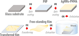
Figure 1. Scheme illustrating the manufacturing, release and transferring process of nanocomposite films.
Download figure:
Standard image High-resolution image2.3. Characterization
The AgNWs colloids and the nanocomposite films were characterized by thermogravimetric analysis (TGA) and differential scanning calorimetry (DSC), DSC Linset PT-1600, transmission electron microscopy (TEM) using a Philips CM200 at 200 kV, scanning electron microscopy (SEM) Zeiss Crossbeam 320, in either secondary electron scanning and scanning TEM (STEM) mode. Topography and conductive-tip atomic force microscopy (CAFM) images were acquired with a Solver Pro NT-MDT Scanning Probe Microscope. The thickness of the films was determined by using a mechanical stylus profilometer Tencor Instruments and an optical profilometer Veeco Wyko NT1100 on films transferred to a glass substrate and then metalized with a silver coating using a Tedpella Sputter coater Cressington 108 AutoSputter Coater.
The electrical properties of the free-standing nanocomposite film were studied with a Keithley 2450 Source Measure Unit. The transmittance was evaluated at 550 nm using a UV–visible spectrophotometer Biotraza 752. Four probe measurements were performed to obtain the sheet resistance [20]. The strain dependent resistance was evaluated using a homemade flexure test machine. A sample of the free-standing film transferred to a polyethylene terephthalate (PET) substrate was placed and the two-probe resistance was registered during repeated bending cycles from −17° to 17°, where 0° is the strain-free position.
3. Results and discussion
Statistic counting of the AgNWs length and diameter is presented in figure S2 (supporting information). A normal distribution fit on the histograms shows a maximum population of AgNWs with (120 ± 40) nm in diameter and (20 ± 10) µm in length; although a population of wires longer than 60 µm is observed, which have a major effect on electrical percolation [21]. AgNWs were used in the preparation of the nanocomposite resist and the formation of films on a PVP sacrificial layer as described in section 2.
After completing the release process, the nanocomposite films were transferred to different substrates for their characterization. A sample was transferred to a glass slide for optical imaging in dark field mode (figure 2(a)), or to a silicon wafer for SEM imaging as shown in figures 2(d) and (e), respectively. Another sample of the free-standing film was transferred to a copper grid for STEM characterization. Here, the sample is observed with a SEM microscope obtaining images under both secondary electrons (figure 2(b)) and transmitted electrons (figure 2(c)). Secondary electrons provide images of AgNWs on the surface of the film, therefore the presence of additional wires underneath could only be detected in transmission mode. Interestingly, no additional wires were observed, indicating that the thickness of the free-standing films was of the order of the diameter of the AgNWs and that the conductive network is formed by a single layer of AgNWs. SEM and STEM images also show the presence of bubbles or pores that are probably the result of a phase separation of the different solvents present in the nanocomposite resist during their evaporation [22]. The formulation of a stable colloid with rheological characteristics suitable for film formation by spin coating represents a considerable challenge. Here, we have worked with formulations containing, in addition to the nanowires and the polymer, co-solvents such as ButAc and ButOH in the stated proportions. The porosity of the final dry-film morphology is dictated mainly by the rate of evaporation and demixing of the different solvents as studied by Schaefer et al [22]. The spin coating process involves a very high evaporation rate followed by a slower rate during the subsequent heat treatment at 90 °C. Pore formation is presumed to occur during these processes, although further studies are needed on this point. A pore-size distribution histogram obtained from STEM and atomic force microscopy (AFM) images is presented in figure S3 (supporting information). TEM images of a single AgNWs in high magnification are presented in figures 2(f) and (g). A thin layer (ca. 1.5 nm) of PVP remaining from the polyol synthesis is highlighted.

Figure 2. (a) Optical microscopy images in dark field mode. STEM images of free-standing films of AgNWs-PMMA constructed from (b) secondary electrons and (c) transmitted electrons. (d) and (e) SEM images of a film transferred to a silicon wafer, (f) and (g) TEM image of a single AgNWs. A surrounding PVP thin layer is highlighted.
Download figure:
Standard image High-resolution imageThe formulation of the nanocomposite aimed to achieve electrical percolation in the network of AgNWs. With this goal in mind, the mass concentration of the AgNWs in the stock solution in IPA was measured by TGA using an isothermal run at 90 °C and a volume of colloid of 50 µl. The measurement was performed three times (figure S4 supporting information). An average mass concentration of (1.0 ± 0.6) g l−1 was obtained, corresponding to a concentration of AgNWs in the nanocomposite resist of (3.5 ± 1.0) g l−1. These concentrations are in accordance with previously reported values for achieving electrical percolation [9, 12, 15, 23].
In addition, DSC was also used to analyze the thermal degradation of the nanocomposite resist and PMMA resist as shown in figure S5 (supporting information). A broad and small endothermic dip at approximately 165 °C for the pure PMMA resist and at 200 °C for the nanocomposite was observed. These dips can be assigned to the glass transition temperature (Tg) of the polymer. A decomposition temperature of 350 °C was measured for a neat PMMA followed by an exothermic peak due to combustion [24]. For the AgNWs-PMMA nanocomposite the decomposition temperature was 360 °C. Both shifts of the characteristic temperature indicate a weak enhancement of the thermal stability of PMMA due to the incorporation of the AgNWs.
3.1. Using the free-standing films
The fabrication procedure described in section 2 (figure 1) made possible to transfer the films to different substrates. Thus, we successfully transferred the films to a flexible PET sheet, a polyimide film, a rigid plastic frame, a nitrile glove, a printed circuit board (PCB) through-hole board (figure S6, supporting information), a curved glass surface (test tube) and between a gap formed by two metallized glass substrates. Once the films are dry, an excellent adhesion provided by van der Waals forces was achieved to all of the surfaces tested. A set of pictures of the different materials explored is shown in figure 3. These samples were used for different purposes. Films transferred to polyimide frames were used to easily manipulate the films while retaining their flexibility. Rigid frames allowed the direct study of the physical properties of the free-standing films and as a tool to transfer them to other substrates. Films on PET were used to study the change in electrical resistance under strain by performing bending cycles, while through-hole PCB boards were used as a multi-electrode framework for the direct measurement of electrical resistance through back contacts, as explained in the next section.

Figure 3. Photographs of the free-standing films transferred to different surfaces. (a) Glass; (b) printed circuit board; (c) PET sheet; (d) a curved surface (test tube); (e) nitrile glove; (f) free-standing films with a PDMS coating on a rigid frame.
Download figure:
Standard image High-resolution image3.2. Physical properties of the nanocomposite free-standing films
Structural characterization of the film was performed in order to obtain the film thickness, its surface roughness and its microstructure. This was performed by multiple techniques including optical and mechanical profilometry, and AFM. Figure 4(a) shows a color-scale image obtained by optical profilometry of a border of the film transferred to a glass substrate. The height profile in figure 4(b) shows the step edge of the film giving (440 ± 40) nm. After averaging the measurements obtained in different regions of the sample, we obtain a mean thickness of (420 ± 30) nm. Stylus profilometry was employed to confirm the film thickness, obtaining (460 ± 20) nm as shown in figure 4(d), which agrees, within the margin of error, with that obtained by optical profilometry. In order to study the effect of the spinning velocity on the resulting thickness of the nanocomposite films, we prepared a series of samples on bare glass substrates and PVP-covered glass substrates by spin coating at different speeds. We measured the film thickness by stylus profilometry before and after the release of the film. Results are shown in figure 4(e). AFM in tapping mode was also employed for the analysis of the film thickness (figure 4(f)) finding a continuous surface that made possible to evaluate the overlap between both sides of the film, resulting in an abrupt step lower than 650 nm (figure 4(g)). As the film is folded on itself, under these conditions the observed height difference is the sum of the irregularities of each layer and their spacing, not being comparable to the values obtained by profilometry.
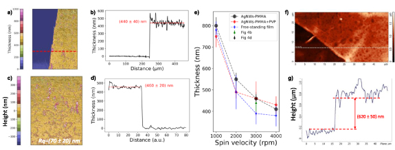
Figure 4. (a) Optical profilometry performed on an edge of a nanocomposite film transferred to a glass substrate; (b) height profile across the highlighted line in (a). Mean and standard deviation are indicated. (c) Topography of the exposed surface of the film for surface roughness analysis. (d) Stylus profilometry on an edge of a nanocomposite film transferred to a glass substrate; (e) effect of spin velocity during deposition of nanocomposite resist on bare glass substrates and PVP-covered glass substrates. Film thickness was measured by stylus profilometry before and after the release of the film. Values reported in panels (c) and (d) are included as black and green triangles, respectively (the reported uncertainties are one-standard deviation statistical uncertainty). (f) AFM scan on a film edge folded on itself; (g) height profile across the line highlighted in (f).
Download figure:
Standard image High-resolution imageThe surface roughness was also studied by optical profilometry (figure 4(c)) showing characteristic roughness of Ra = (50 ± 10) nm and Rq = (70 ± 20) nm for the arithmetic and quadratic averages, respectively. These high values are in accordance with the porous structure of the films shown in figure 2 and explain the low optical transmittance.
A deeper analysis of the topography was performed by AFM, showing a sponge-like structure pierced by the AgNWs in figure 5(a). This idea is reinforced by the corresponding phase contrast image (figure 5(b)) which suggests that some of the wires remain partially accessible over the PMMA. Figure 5(d) displays CAFM measurements between the Pt tip and a silver paint top electrode, placed about 1 cm away from the scanned area. Local current was mapped with a bias voltage of 2 V, along with its contact mode topography image (figure 5(c)), showing that these wires are also electrically accessible and part of a long range electrical conduction through the AgNWs-PMMA matrix.
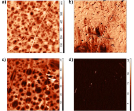
Figure 5. AFM images of the exposed surface of a nanocomposite film transferred to a glass substrate. (a) Topography in tapping mode, (b) phase mode image; (c) topography in contact mode and the corresponding current profile (d) obtained by CAFM with a bias voltage of 2 V. Scanned windows is 20 µm × 20 µm in all cases.
Download figure:
Standard image High-resolution imageThe electrical properties of the nanocomposite films were studied by performing two-point I–V sweeps or by direct four-probe resistance measurements. In this last case, four contact slots of silver paste were deposited on the samples before the release of the films. We could control the sheet resistance of the samples by tuning the concentration of wires reaching values down to 45 Ω sq−1. However, the standard system used in all samples showed a sheet resistance obtained by two-probe method of (670 ± 40) Ω sq−1 for the free-standing films.
An optical transmittance at 550 nm of (78 ± 1)% was measured on a self-supported film transferred to a plastic frame for manipulation. The transparency of the films can be appreciated in figure 3.
By transferring a sample on top of two metallized glass slides separated by a gap distance of ca. 1 mm (inset figure 6), forming a bridge-like structure, it was possible to study the resistance of the free-standing film by two-point I–V sweeps. An ohmic behavior was measured with a resistance of 51 Ω, with no changes visualized at currents up to 20 mA (figure 6). A table summarizing our results in comparison with other similar works [13, 25, 26] is presented in table S1, supporting information.
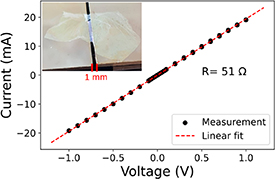
Figure 6. I–V curve of free-standing membrane with a separation of 1 mm. An ohmic behavior of 51 Ω was observed. Inset: photograph of the system.
Download figure:
Standard image High-resolution imageIn addition, the electrical properties of the nanocomposite films were studied by transferring the free-standing films to a PCB through-hole board. The film covered 3 × 5 electrodes in a square array with a pitch distance of 0.1 inch (2.54 mm). By contacting the back side of the board, we measured the resistance between each electrode and the central one in order to build the resistance map shown in figure 7. An ohmic behavior was measured for all pairs of electrodes. It is interesting to note that the resistance is not uniform across the film, with lower resistance values measured, in this case, on the top-left regions of the film. The topology of the percolating network, having fluctuations in the local concentration of AgNWs, may explain the non-uniform conductivity. Ideally, transferring the film on top of a multi-electrode array with a smaller pitch would allow the construction of a conductance map with a higher resolution that can be correlated with the network topology observed by optical microscopy.
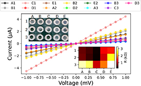
Figure 7. I–V curves measured between indexed electrodes and the reference (C2) of a nanocomposite film transferred to a through-hole PCB board with a square array of electrodes 0.1 inches apart. E3 presented a resistance value higher than the instrumental resolution. Top inset: photograph of the sample; bottom inset: resistance map constructed from the I–V curves.
Download figure:
Standard image High-resolution image3.3. Stacking of free-standing films
An important capability of the developed method for releasing and transferring free-standing films is the formation of stacks by piling up successive layers of the conductive nanocomposite. This would enable the realization of out-of-plane circuitry and also the covering of large areas by a mosaic arrangement of conductive patches. Transferring a free-standing film on top of another raises the question if the contact resistance is high enough to block the conductance or, on the opposite, a conduction path is established between stacking films. In order to answer this question a proof of concept test was realized by first depositing a stripe of the film on a glass substrate and then a second stripe was deposited partially covering the previous one. Optical microscope images can be seen in figures 8(b) and (c). Figure 8(a) shows I–V curves measured along a single stripe or through the connection between the two stripes. We measured a two-probe resistance of 1.5 kΩ in the former case and 10.1 kΩ for the latter. This result indicates that, although a high contact resistance exists between the two layers, an ohmic conductivity is retained, enabling the design of 3D architectures. This is consistent with the CAFM images (figure 5(d)), suggesting that the electric contact is only driven between some outer wires of both surfaces that casually got in mechanical and electrical contact. This would enable the design of 3D architectures.
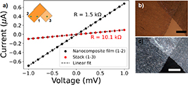
Figure 8. (a) I–V curves of a free-standing film and a stacking of them. Ohmic behavior was observed in both systems. (b) Brightfield and (c) darkfield mode light microscopy image of the stacking zone. Scale bars are 200 µm.
Download figure:
Standard image High-resolution image3.4. Free-standing membranes with a PDMS coating
The mechanical robustness of the free-standing films can be greatly enhanced by adding a second layer with high flexibility. Here, we tested the incorporation of a thin layer of PDMS produced by spin coating a 10:1 mixture of the Sylgard 184 PDMS kit on top of the nanocomposite as an additional step, following step 3 of the fabrication process depicted in figure 1. The deposited PDMS layer was thermally cured at 80 °C for 2 h before the release process (step 4, figure 1). By adding a small layer of PDMS, a conductive film with enhanced robustness was obtained. This facilitates greatly the manipulation of the film for its operation as a free-standing conductive film. We employed a plastic frame with a 1 cm × 1 cm open center to deposit a sample of the PDMS reinforced nanocomposite film (figure 3(f)). A resistance of the order of 10 kΩ was observed between contacts at a distance of about 1 cm.
3.5. Strain sensitive resistance
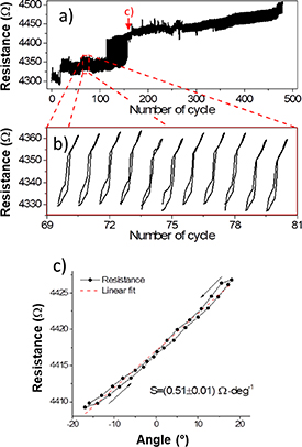
The sensitivity of the nanocomposite films to deformations and strain was tested by transferring the film to a PET sheet (105 ± 5) µm thick. A stripe of the sample (4 mm × 20 mm) was placed in a homemade motorized bending machine where it was submitted to bending cycles from −17° to 17° around a 4 mm radius axis. The results are shown in figure 9. Upon multiple cycles, the strain-free resistance of the film (at 0° bending) shows a progressive increment denoting a gradual damage of the AgNWs network (figure 9(a)). Sudden increases in the resistance occurred during the experiment, also pointing towards irreversible changes in the network. Individual cycles show an increase (decrease) in the resistance under tension (compression); however, the first cycles present a hysteretic behavior with a non-linear response (figure 9(b)). After approximately 100 cycles, the response become linear with a sensitivity to deformation of (0.51 ± 0.01) Ω deg−1 as calculated from data shown in figure 9(c).
Figure 9. Flexion tests performed on a nanocomposite film transferred to a PET sheet; (a) resistance measured under automated bending cycling from −17° to 17°; (b) detail view of bending cycles during the first stage of the essay; (c) example of a single bending cycle indicated with in panel (a) showing a linear response. Arrows indicate the direction of the bending test. The sensitivity was calculated as the slope in a linear fit.
Download figure:
Standard image High-resolution image
Clearly, the system will not be suitable for the construction of macroscopic strain sensors until stability is improved. Different strategies and further tests are underway to achieve these goals. However, the change in electrical resistance upon deformation of the film becomes interesting for sensing the structural stability of free-standing membranes, for the construction of gas pressure sensors, polymer MEMs and highly sensitive mechanical fuses.
4. Conclusions
We presented a method to produce large-area free-standing thin films formed by a percolative network of self-assembled AgNWs within a PMMA matrix. Under the studied conditions, the films show a sheet resistance of (670 ± 40) Ω sq−1, an optical transmittance of 78% and a film thickness of approximately 450 nm. We explored different possibilities for the application of the nanocomposite films and their transferring to non-flat surfaces that are not easy to coat by other means. We showed that curved surfaces and different materials like nitrile, PET and glass can be covered with excellent adhesion of the film. The electrical properties of the films were evaluated by means of bending tests obtaining a high-sensitivity response to flexion. The formation of multilayer stacking showed conductivity across stacked films. By adding a PDMS covering layer we improved the robustness of the films and facilitated their manipulation.
With these proof-of-concept tests, we intend to provide a novel strategy for the advancement of various developing technologies of current interest, such as artificial skin, biocompatible sensors, microelectromechanical devices and neuromorphic systems, among others.
Acknowledgments
Authors would like to thank Dra. Paula Angelomé (GQ-CAC-CNEA) for TGA measurements, Antonela Geuna (FQ-CAB-CNEA) for DSC measurements, Carlos Bertoni (GIA-CNEA) for his assistance in SEM and STEM imaging and Dr Alfredo Tolley (GF-CNEA) for his assistance in TEM imaging. We acknowledge funding from National Agency for the Promotion of Science and Technology (ANPCyT) through grant PICT Start Up 2019-00017. J I D S acknowledges fellowship from CONICET.
Data availability statement
The data that support the findings of this study are available upon reasonable request from the authors.
Supplementary data (1.0 MB PDF)