


Abstract
Organic photovoltaic (OPV) devices have the potential to be superior to other PV technologies for the use in applications that require very high flexibility or maximum specific power (power-per-weight ratio), such as textile integration, wearable electronics, or outer space applications. However, OPV devices also require encapsulation by barrier films to reduce the degradation driven by extrinsic factors, which in turn limits their flexibility and leads to lower specific power values. In this work, fully solution-processed (including both electrodes) semitransparent organic solar cells (OSCs) with performance comparable with conventional indium tin oxide-based devices are processed directly onto different barrier films of varying thicknesses. Direct cell fabrication onto barrier films leads to the elimination of the additional polyethylene terephthalate substrate and one of the two adhesive layers in the final stack of an encapsulated OPV device by replacing the industrial state-of-the-art sandwich encapsulation with a top-only encapsulation process, which yields significantly thinner and lighter 'product-relevant' PV devices. In addition to the increase of the specific power to 0.38 W g−1, which is more than four times higher than sandwich-encapsulated devices, these novel OSCs exhibit better flexibility and survive 5000 bending cycles with 4.5 mm bending radius. Moreover, the devices show comparable stability as conventionally encapsulated devices under constant illumination (1 sun) in ambient air for 1000 h. Finally, degradation under damp heat conditions (65 °C, 85% rh) was investigated and found to be determined by a combination of different factors, namely (UV) light soaking, intrinsic barrier properties, and potential damaging of the barriers during (laser) processing.
Export citation and abstract BibTeX RIS

Original content from this work may be used under the terms of the Creative Commons Attribution 4.0 license. Any further distribution of this work must maintain attribution to the author(s) and the title of the work, journal citation and DOI.
1. Introduction
Organic solar cells (OSCs) have undergone an impressive development over the last 20 years and by now have reached certified power conversion efficiencies (PCEs) up to 18.2% for small lab-scale devices [1, 2]. Even though the PCEs are still below those of conventional PV technologies, there are key features raising both academic and industrial interest in OSCs. On one hand, full solution-processability and compatibility with roll-to-roll (R2R) production make OSCs highly industry-relevant due to the possible low manufacturing costs and short energy payback times together with high throughput. However, a majority of the reported architectures with high efficiencies are constituted by interlayers and/or electrodes processed with high vacuum techniques such as thermal evaporation [3–5]. Especially, indium tin oxide (ITO), which is a commonly used transparent electrode in such architectures, is one of the main cost drivers, since it is manufactured by energy-intensive vacuum processes and indium is a scarce element [6]. Therefore, solution-processable bottom electrodes are necessary for simple, low-cost, and high-throughput manufacturing. Among several alternatives, silver nanowires (AgNWs) stand out, owing to the simultaneous provision of high optical transparency and electrical conductivity by metallic mesh networks [7]. In addition, it is well-established that OSCs with AgNW bottom electrodes can reach PCEs comparable to those of ITO-based devices [7–10].
OSCs are superior or even unique compared to other PV technologies when it comes to flexibility, light weight, and freedom in shape. With these properties, OSCs enable the implementation of solar power wherever needed, leading to new application possibilities such as textile integration (e.g. onto backpacks, umbrellas, tents...) and wearable electronics powered by solar energy or ambient lighting. For the fields in which reduction in weight is crucial (e.g. outer space applications), specific power (power-per-weight ratio, W g−1) is a valid measure [11]. To this regard, the use of ultrathin substrates results in ultrathin, super light-weight, and high specific power devices, as the weight of an organic photovoltaic (OPV) device is almost equivalent to the substrate weight due to the negligible weight and thickness of the actual solar cell stack [12, 13]. For example, Bihar et al fabricated a PH3T:O-IDTBR-based fully printed OSC onto a 1.7 μm thick parylene substrate and achieved a power-per-weight ratio of 6.3 W g−1 with 3.6% PCE [14]. Such ultrathin polymer substrates not only improve specific power but also lead to ultra-flexible, bendable, stretchable, and compressible devices [15].
Thus far, reported ultrathin solar cells have reached 13.0% PCE while offering extreme flexibility in both bending and compression-stretching conditions [12, 16–18]. Nevertheless, despite all these accomplishments, there are certain aspects that cannot be overlooked in order to make the use of such devices commercially widespread. Firstly, such thin substrates possess insufficient tensile strength to withstand the required web tension of a R2R production process [19]. Secondly, it is an obstacle for these light-weight and ultraflexible OSCs to achieve good environmental stability since ultrathin substrates have no real barrier effect against gas permeation. Although there are studies establishing 'barrier films' and still maintaining total device thicknesses below 3 μm, such protective layers by far cannot offer the gas barrier properties required for an OPV device (⩽10−4g m−2 d−1 water vapor transmission rate (WVTR) and ⩽10−3cm−3 m−2 d−1 atm oxygen transmission rate (OTR)) [15, 20, 21]. Consequently, these devices cannot provide long-term stability under ambient environmental conditions. Recently, Jiang et al developed an ultraflexible OPV device with good environmental stability (extrapolated T80 shelf lifetime of 20 750 h, stored in the dark under ambient conditions); however, the reported lifetime values refer to glass-encapsulated cells, which means the device is no longer light-weight and flexible [22]. To this end, a proper encapsulation needs to be adapted for long-term stability without compromising the benefits of ultrathin OSCs.
In this report, we present fully solution-processed and semitransparent OSCs with AgNW bottom and top electrodes. This double-AgNW architecture not only provides R2R-compatibility, but also enables the fabrication of such devices onto any kind of substrate. This is proven by processing the solar cells directly onto different barrier films of varying thickness. By using this strategy, the traditional sandwich encapsulation method (i.e. laminating the OPV device between two barrier foils by means of an adhesive) is replaced by a top-only encapsulation, which eliminates an additional substrate and one of the two adhesive layers from the final device stack and, in turn, increases the specific power of these industry-relevant encapsulated OPV devices [23–25]. The flexibility of these devices is examined by a bending test. Furthermore, the devices are subjected to accelerated lifetime tests, namely constant illumination (ISOS-L-2) and damp heat (ISOS-D-3), in order to assess their long-term stability under real-life operation conditions [26]. A detailed analysis of the degradation behavior by imaging techniques reveals the Achilles' heels of the devices and defines the strategy for optimal processing and encapsulation.
Overall, this work describes the most advanced industry-relevant OSCs combining the key aspects of high power-to-weight ratio, elimination of indium, R2R-processability on discretionary surfaces, semitransparency, ultraflexibility, and longevity.
2. Experimental details
2.1. Materials
The standard substrates utilized in this work are based on heat-stabilized polyethylene terephthalate (PET) (DuPont Teijin Films, Melinex® ST504). The 'IMI' substrates comprise the same PET substrate but contain a transparent conductive coating of ITO–Ag–ITO and were purchased from OPVIUS. A PET-based standard barrier film including UV cut-off filter ('SB + UVF', X-Barrier VD-K3DA) was purchased from Mitsubishi Chemical. Three additional barrier films ('SB', 'HB + UVF', and 'HB') have been provided by Mitsubishi Chemical as research samples. Details about UV and visible light transmittance, thickness, and water permeability of the different foils are summarized in table 1.
Table 1. UV–Vis transmission properties, thicknesses, and WVTRs of the different foils used in this work.
| Name | UV filter | Transmittance @550 nm (%) | Thickness (μm) | WVTR (g m−2 d−1) |
|---|---|---|---|---|
| PET | — | 87.5 | 125 | 4 |
| SB + UVF | <1% T below 378 nm | 78.1 | 65 | 5 × 10⁻³ |
| SB | — | 88.2 | 23 | 8 × 10⁻³ |
| HB + UVF | <1% T below 375 nm | 86.1 | 107 | 8 × 10⁻⁴ |
| HB | — | 87.6 | 83 | 7 × 10⁻⁴ |
The active materials poly(3-hexylthiophene) (P3HT) and (5Z,5'Z)-5,5'-((7,7'-(4,4,9,9-tetraoctyl-4, 9-dihydro-s-indaceno[1,2-b:5,6-b']dithiophene-2, 7- diyl)bis(benzo[c][1,2,5]thiadiazole-7,4-diyl))bis(methanylylidene bis(3-ethyl-2-thioxothiazolidin-4-one) (O-IDTBR) were purchased from OPVIUS and Nano-C, respectively. The solvents used to dissolve the active layer materials were o-xylene (o-XY, Sigma-Aldrich) and 1-methylnaphthalene (1-MN, Merck). The interlayers, aluminum-doped zinc oxide (AZO, N-21X) and poly(3,4-ethylenedioxythiophene)-poly(styrenesulfonate) (PEDOT:PSS) (HTL Solar) were purchased from Avantama AG and Heraeus, respectively. Finally, isopropyl alcohol based AgNW ink was purchased from Cambrios.
2.2. Device fabrication
All layers are coated in ambient air using a doctor blade from Zehntner. For the preparation of the reference device (PET/IMI/AZO/P3HT:O-IDTBR/PEDOT:PSS/AgNW), the PET/IMI substrates are patterned with a fs-laser (LS Laser Systems) with 350 fs pulse duration, 520 nm wavelength, and 0.40 J cm−2 fluence to electrically separate the bottom electrode. The laser-patterned PET/IMI substrates are cleaned mechanically with a microfiber tissue and toluene to get rid of the debris caused by lasering, followed by an ultrasonic bath in 2-propanol for 10 min. All cleaned substrates are coated with AZO nanoparticles (NPs) as the electron transport layer (ETL) and annealed at 120 °C for 30 min. The active materials solution, P3HT:O-IDTBR (1:1.5) in o-XY:1-MN (19:1), is stirred over night at 80 °C and coated at 65 °C. The hole transport layer, PEDOT:PSS, is coated at 65 °C followed by an annealing step at 140 °C for 4 min under inert atmosphere. Subsequently, the AgNW top electrode is coated at 65 °C with ∼5 Ω sq−1 sheet resistance. After coating the top electrode, a final laser patterning step is conducted with 0.18 J cm−2 fluence to establish six individual cells, each with 0.1 cm2 cell area, on each substrate. Finally, the samples are annealed again at 120 °C for 4 min under inert atmosphere. For the preparation of samples with AgNW bottom electrode, all substrates (PET and barrier foils) are cleaned in 2-propanol for 10 min by using an ultrasonic bath. After cleaning, a layer of AZO NPs is deposited on top of which the AgNWs are coated at 65 °C resulting in a sheet resistance of ∼10 Ω sq−1. Then, an annealing step at 120 °C for 5 min is carried out. The rest of the processing steps are identical to the reference cell fabrication mentioned above.
For degradation and bending tests, the solar cells fabricated on standard PET substrates (without barrier properties) are sandwich-encapsulated with a commercial barrier foil ('SB + UVF', see table 1) from top and bottom by means of a UV-curable glue (LP655 from DELO) and a laminator from Fetzel Maschinenbau. The solar cells fabricated directly on different barrier films are encapsulated only from the top side, always using the same foil as was also used as substrate.
All PET-based substrates and barrier foils used in this work were compatible with processing temperatures up to 140 °C without showing any signs of damage or deformation. However, it is beneficial to slowly ramp the temperature up and down rather than applying fast temperature jumps and it is important to actively flatten the samples when placing them on a hot plate in order to prevent bending, especially for the very thin barrier foils.
2.3. Stability tests
Accelerated lifetime tests of the encapsulated devices were performed under two different conditions. Firstly, one set of samples was placed in a Suntest chamber by ATLAS and exposed to the light of a xenon lamp (AM 1.5, 1000 W m−2) for 1000 h, which corresponds to ISOS-L-2 conditions. Secondly, another set of samples was placed in a climate chamber by ESPEC exposing it to damp heat (65 °C, 85% relative humidity) for 1000 h, which corresponds to ISOS-D-3 conditions. During the lifetime tests, electrical measurements of the PV devices were performed approximately every 150 h.
Flexibility tests were conducted by a self-made bending machine including one stationary and one movable part, which moves back and forth linearly. The samples are clamped into these two parts, with both of them being able to rotate, causing a repetitive stress cycle of bending (∼4.5 mm radius) and relaxation (flat) to the solar cell.
2.4. Characterization
A UV–Vis spectrometer (UV1800, Shimadzu) with an operating range from 190 to 1100 nm is used to acquire transmittance data of the substrates and the transparent electrodes. For the investigation of the patterning and ablation of the layers, an optical microscope (Olympus MX51) enabling bright- and dark-field imaging is used. Electroluminescence (EL) imaging is used to inspect the degradation behavior of the solar cells. For the excitation, 1.5 V forward bias was applied to the cells by using a source unit (Keysight B2901A, Keysight Technologies). For the imaging, a Ninox VIS-SWIR 640 camera (Raptor Photonics) and an air-cooled indium–gallium–arsenide detector with a sensitivity of 0.4–1.7 μm were used. EL images were captured with an exposure time of 5 s. The sheet resistances of the electrodes were measured by a non-contact sheet resistance meter from DELCOM Instruments. The JV characteristics of the solar cells are measured by using a source measure unit (Keysight B2901A, Keysight Technologies) and a class AAA solar simulator (LOT Quantum Design) providing AM 1.5 G illumination of 1000 W cm−2.
3. Results and discussion
3.1. Optimization of fully solution-processed semitransparent OSCs
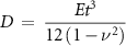
As a starting point, the industry-relevant active layer system P3HT:O-IDTBR was chosen, since it can be deposited from green solvents (e.g. o-xylene), performing comparably with a processing from halogenated solvents (e.g. chlorobenzene) [27]. PEDOT:PSS was selected as hole transport layer together with a AgNW top electrode as it provides sufficient lateral conductivity to bridge the voids of the AgNW mesh while offering a proper carrier selectivity [28, 29]. AgNWs constitute the state-of-the-art material for solution-processed transparent top electrodes. Moreover, it has also been reported in the literature that AgNWs are a promising candidate for the bottom electrode [7–9]. However, regarding the latter there are several issues inhibiting their application, such as shunting of the devices due to the tendency of NWs to form agglomerates and the difficulty in extracting charges generated in the center of the AgNW mesh voids, especially for inverted device architectures [10]. To this end, we pursue a co-optimization of the bottom electrode and the ETL. The optimization is realized in three steps: (a) adjustment of the ETL thickness for concomitant optimization of the parallel resistance Rp and the series resistance Rs, (b) improvement of the AgNW-ETL contacting area for reducing Rs, and (c) enhancement of charge transport by UV-light activation. The best results of each optimization step are shown in figure 1(a) and table 2.

Figure 1. (a) Current density vs bias curves of P3HT:O-IDTBR based solar cells after each optimization step: the reference cell with IMI electrode and 100 nm AZO (black), a cell with AgNW bottom electrode and 100 nm AZO (purple) on top, a cell with AgNW electrode being embedded between two AZO layers (green), and the latter device being light-soaked for 30 min (red). (b) Sketch of the fully optimized solar cell stack. (c) Photograph and transmission spectrum of the complete solar cell stack (including 125 µm PET substrate).
Download figure:
Standard image High-resolution imageTable 2. Short-circuit current (Jsc), open-circuit voltage (Voc), fill factor (FF), and PCE of the PV devices after each optimization step (average of six cells per variation).
| Electrode/ETL | Light soaking duration (min) | Jsc (mA cm−2) | Voc (V) | FF (%) | PCE (%) |
|---|---|---|---|---|---|
| IMI/AZO | 3 | 11.84 (±0.26) | 0.69 (±0.00) | 70.01 (±0.45) | 5.76 (±0.08) |
| AgNW/AZO | 3 | 11.62 (±0.59) | 0.69 (±0.00) | 58.94 (±1.02) | 4.72 (±0.16) |
| AZO/AgNW/AZO | 3 | 11.84 (±0.17) | 0.69 (±0.00) | 62.56 (±1.03) | 5.17 (±0.11) |
| AZO/AgNW/AZO | 30 | 12.10 (±0.28) | 0.68 (±0.00) | 66.77 (±1.61) | 5.52 (±0.18) |
First, aluminum-doped zinc oxide (AZO) is selected as ETL because of its superior conductivity compared to other well-known ETL materials (e.g. ZnO or SnO2), which enables processing of thicker layers without negatively affecting the solar cell performance [30]. Further, the thickness of AZO is optimized regarding a maximum charge extraction and a minimum leakage current. The 50 nm thick AZO layers lead to insufficient surface planarization of the AgNW network, which results in a low parallel resistance (Rp, slope of the dark JV curve at −0.5 V) of 0.9 × 10⁴Ω cm2 and a consequent drop in fill factor (FF) to ∼56% due to a slight shunting of the devices (figure S1 and table S1 available online at stacks.iop.org/FPE/7/025003/mmedia). When a 100 nm thick AZO layer is coated, Rp increases more than three times (3.1 × 10⁴ Ω cm2) and the FF increases to ∼59%. Finally, increasing the AZO thickness to 150 nm does not further improve Rp and FF, but reduces the Jsc significantly and thus causes an overall PCE loss to ∼4.5%. Consequently, an AZO thickness of 100 nm is chosen for all following devices.
Second, a low contact resistance between AgNW and ETL is essential, due to the only ∼10% surface coverage of AgNWs at 90% transparency of the bottom electrode, which leads to a very high current density at the points of charge extraction from the AZO layer to the AgNW mesh. The contact resistance between the bottom electrode and the ETL is thus strongly influenced by the effective contact area between the two materials. This effective contact area may be especially low in the case of AZO NPs and AgNWs, since both nanostructures exhibit curved surfaces due to their spherical or rod-like shape, respectively. Therefore, embedding the AgNWs into an AZO matrix by coating an additional 50 nm layer of AZO NPs underneath the AgNW layer (see figure 1(b)) may decrease the NW-NP contact resistance by increasing (almost doubling) the effective contact area. Indeed, the series resistance is found to decrease, as can be seen in the JV curves of the cells with (green) and without (purple) an additional AZO layer below the AgNWs (figure 1(a)), which in turn leads to higher FF (∼63%) and PCE (∼5.2%) values (see table 2). Additionally, as it has already been reported by Morgenstern et al, embedding the AgNWs into a fully surrounding AZO matrix provides a beneficial effect on the temperature stability of the AgNW electrode [31]. We were able to reproduce and confirm this behavior by annealing bare and AZO-embedded AgNW films at high temperatures, finding that the bare AgNW networks decompose at temperatures higher than 160 °C, which results in a steep increase in sheet resistance, while the AZO-embedded AgNW network remains stable up to 280 °C (figure S2(a)). Optical microscope images (figures S2(b) and (c)) reveal melting of the AgNWs if not being embedded. Ramasamy et al explain the increased thermal stability with the increased melting temperature of the crystal embedded into a matrix of a higher melting temperature and a matching lattice parameter due to the inhibited movement of the surface silver atoms [32, 33].
Finally, the effect of light soaking is investigated since the AZO conductivity is known to improve upon (UV-) light treatment [34]. We find that the PCE of our devices when being measured at 1000 W m−2 (AM1.5G) directly after light exposure (i.e. no light soaking) is rather low (∼3.0%), but steadily increases with illumination time (see figure S3). The maximum PCE (∼5.5%) is finally reached after 30 min of light soaking (see figure 1(a) and table 2). The reason for this behavior is an initially high series resistance that decreases upon irradiation. An additional experiment (see figure S4) reveals that the origin of this series resistance increase is indeed the aforementioned increase in AZO conductivity rather than a reduced sheet resistance of the AgNW/AZO bottom electrode. This result suggests that without light soaking the cell performance is mainly limited by a hampered vertical charge transport through the 100 nm thick AZO layer. The especially pronounced need of light soaking for devices with AgNW/AZO bottom electrodes can be explained by the fact that, in comparison with devices comprising bottom electrodes with full-area coverage (e.g. IMI), charges have to pass a longer mean distance through the AZO, because they do not only have to be transferred vertically but also laterally through the AZO layer until they reach the closest connection point to the AgNW network. Finally, it is to note that the observed light soaking effect is not permanent but deactivates automatically upon storage in the dark (see figure S4), which makes it unfortunately not possible to make this UV-light treatment part of the production process.
In conclusion, it can be seen from figure 1(a) and table 2 that the optimized fully solution-processed solar cells with AgNWs as bottom and top electrode exhibit similar performance as the reference cell with IMI as bottom electrode. Furthermore, the processing yield (i.e. the cell-to-cell variation on one substrate as well as the substrate-to-substrate variation in one experimental run) and the reproducibility (i.e. the batch-to-batch variation between different experimental runs) of these devices is found to be very good (see figure S5). The corresponding optimized layer stack, as it is used for the rest of this study, is depicted in figure 1(b). The respective transmission spectrum of this layer stack (including a 125 µm PET substrate) is shown in figure 1(c) together with a photograph, which demonstrates very good optical transparency with an average visible transmittance value of 10.5%. Besides its semitransparency and R2R-compatibility, such a double-AgNW architecture provides additional benefits such as processability onto any kind of substrate, including opaque ones, due to the fact that the top electrode is also transparent. Moreover, this solar cell stack can be printed onto any object, providing PV activity without significantly increasing its weight (only ∼1 g m−2). In the upcoming chapter, we apply this strategy by directly fabricating solar cells onto barrier foils in order to reduce the total device thickness and thereby enhance the specific power of semitransparent OPVs.
3.2. OSCs on and in between barrier foils
For a product-relevant OPV device in both outdoor and indoor use, encapsulation is required to prevent degradation caused by external factors (e.g. oxygen, water vapor, UV-light). The overall goal of this work is to reduce the weight and thickness of such product-relevant devices, and thereby improve their power-per-weight ratio and flexibility. This is achieved by fabrication of a fully solution-processed solar cell stack directly onto a barrier film, thus combining the functionalities of the substrate and of the encapsulation in one foil. Since a regular PET substrate has hardly any barrier effect (4 g m−2 d−1 WVTR and 10 cm3 m−2 d−1 bar OTR) [35], PET/IMI and PET/AgNW based devices need to be encapsulated between two encapsulation foils ('sandwich encapsulation') by application of adhesives from both sides, while the devices processed onto barrier films only need a top encapsulation, as illustrated in figure 2. This newly developed architecture makes the devices significantly thinner, lighter, and potentially also more flexible than the state-of-the-art sandwich encapsulation because one adhesive layer (∼20 µm) and the PET substrate (∼125 µm) are eliminated from the final stack. Concurrently, it is to note that all barrier films are thinner than the commonly used PET substrate, but their tensile strength is still sufficiently high to serve as substrate in a R2R production process (in contrast to, e.g. 3 µm thick parylene films).
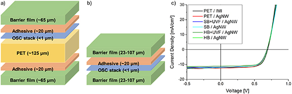
Figure 2. Schematic illustration of the final OPV device architecture using a state-of-the art sandwich encapsulation (a) or the top-only encapsulation developed in this work (b) and JV curves of cells with IMI bottom electrode on PET (black) and AgNW bottom electrode fabricated on PET (red), standard barriers with (dark blue)/without (light blue) UV filter, and high barriers with (dark green)/without (light green) UV filter. All cells are light soaked for 30 min (c).
Download figure:
Standard image High-resolution imageTherefore, in the first step, the optimized solar cell stack (see figure 1(b)) is processed directly onto different barrier foils and the device performances are compared to those of cells being processed onto regular substrates (PET/IMI and PET/AgNW). Four different barrier foils are investigated, which primarily differ in barrier quality in terms of WVTR and UV-light transmission (see table 1 for detailed specifications). Two of the four barriers are standard barriers ('SB') with a WVTR of ∼10−3 g (m2 d)−1, while the other two are high barriers ('HB') with a WVTR of ∼10−4 g (m2 d)−1. Both SB and HB exist in two versions, one without UV filter properties and the other one with an included UV filter ('+UVF') with a cutoff below ∼380 nm. The barrier foil thicknesses range from 23 µm (SB) to 107 µm (HB + UVF).
The properties and performance of the resulting PV devices are shown in table 3 ('before encapsulation'). Firstly, it is to note that both the thickness and the weight of the whole device equal approximately that of the bare substrate, because the actual solar cell stack has a thickness of only ∼0.5 μm and accounts for a specific weight of only ∼1 g m−2, which is negligible compared to the substrate thickness and weight. Secondly, all devices processed directly onto barrier foils perform almost equally in PCE (∼5.3%) and thus similar to the references on PET/AgNW, as can also be seen in the respective JV curves (figure 2(c)). A marginally lower Jsc is observed for barrier films that include a UV filter, which can be explained by the decreased light transmission for those barrier foils cutting off all wavelengths below ∼380 nm (figure S6). Despite their slightly lower PCE, the specific power (i.e. the power-per-weight ratio) of all devices on barrier foils is superior due to their lower thickness and area density. The highest specific power is obtained for the cells on the thinnest/lightest substrate (SB) and equals 1.66 W g−1, which is more than five times that of the cells on a regular PET substrate.
Table 3. Thickness, area density, PCE, and specific power values of the devices before and after encapsulation. The reference cells with IMI and AgNW electrode on a regular PET substrate are encapsulated with standard barrier foil including UV filter (SB + UVF). Cells fabricated on barrier foils (SB, SB + UVF, HB, and UB + UVF) are encapsulated with the same barrier foil they are processed onto.
| Before encapsulation | After encapsulation | |||||||
|---|---|---|---|---|---|---|---|---|
| Substrate | Device thickness (μm) | Area density (g m−2) | PCE (%) | Specific power (W g−1) | Device thickness (μm) | Area density (g m−2) | PCE (%) | Specific power (W g−1) |
| PET (IMI) | 125 | 177.4 | 5.80 (±0.16) | 0.33 | 298 | 475.4 | 5.07 (±0.12) | 0.11 |
| PET | 125 | 177.4 | 5.46 (±0.18) | 0.31 | 299 | 475.4 | 4.60 (±0.13) | 0.09 |
| SB + UVF | 65 | 81.6 | 5.27 (±0.11) | 0.65 | 155 | 233.2 | 5.06 (±0.10) | 0.22 |
| SB | 23 | 32.4 | 5.33 (±0.13) | 1.66 | 85 | 134.8 | 5.16 (±0.11) | 0.38 |
| HB + UVF | 107 | 149.0 | 5.21 (±0.10) | 0.35 | 247 | 368.0 | 4.95 (±0.08) | 0.13 |
| HB | 83 | 110.2 | 5.40 (±0.71) | 0.49 | 188 | 290.4 | 5.26 (±0.77) | 0.18 |
Subsequently, all of the devices are encapsulated. The references (processed on PET/IMI and PET/AgNW) are sandwich-encapsulated with a standard barrier foil including UV filter (SB + UVF) from the top and the bottom (see figure 2(a)), whereas all other devices are encapsulated only from the top (see figure 2(b)) with the same barrier foil they are processed onto. As shown in table 3 ('after encapsulation'), the specific power of all devices is reduced after encapsulation, which is mainly attributed to the increase in device weight (area density). In addition, slight PCE losses are observed for all devices upon encapsulation. Around 15% relative loss is observed for sandwich-encapsulated cells, which can be explained by the fact that in this case a barrier foil (SB + UVF) and a layer of glue are applied to the light-facing side of the device, thus being introduced between the light source and the OSC, which reduces the total amount of light reaching the actual solar cell (see figure S6 for transmission spectra). On the other hand, top-only encapsulated devices only exhibit a PCE loss of ∼4%, which may be the result of photo-oxidation since the device encapsulation is performed in air and involves UV-curing of the glue. The fact that the PCE losses are predominantly caused by a reduction in Jsc (see table S2) further corroborates this hypothesis.
However, as mentioned before, the overall reduction in specific power by a factor of 2.7–4.4 upon encapsulation can be mainly related to the increasing device weight (by a factor of 2.5–4.2). Comparing the final encapsulated devices, the solar cell processed onto and being top-encapsulated with the thinnest barrier foil (SB) yields the highest specific power of 0.38 W g−1, which is a factor of ∼4 higher than the sandwich-encapsulated reference devices.
3.3. Lifetime and stability
3.3.1. Light stability
The stability towards constant illumination (1000 W m−2) of the cells processed on (and top-only encapsulated with) the SB + UVF foils is investigated and compared to that of the reference cells (PET/IMI and PET/AgNW) that are sandwich-encapsulated with the same barrier foil. The barrier foil with UV filter is selected to minimize UV-induced instabilities that lead to faster degradation [36]. A PCE loss of ∼45% is observed for all cells after 1000 h illumination (figure 3), which mainly originates from a decrease in FF by ∼40% (see figure S7). The temporal evolution of the observed degradation is also the same for all variations and starts with a pronounced initial burn-in phase causing ∼30% PCE loss during the first ∼100 h. Possible origins of such degradation are oxygen ingress into the device [37], UV light-induced photoactive layer degradation [38, 39], morphological changes inside the active layer due to elevated temperatures (∼65 °C) [38], and stimulated photocatalytic activity of ZnO [40]. While the overall deterioration may be a combination of these possible degradation mechanisms, we infer that temperature plays the major role, since a similar degradation behavior (∼30% PCE loss within ∼300 h) is observed for cells that are kept on a hot plate at 70 °C in the dark under an inert atmosphere (figure S8). It is to note at this point that we have previously shown P3HT:O-IDTBR to be stable for 2000 h upon illumination with an LED light source (1000 W m−2, no UV content) that avoids heating of the devices [41].

Figure 3. Normalized change in PCE of sandwich-encapsulated cells with IMI (black), sandwich-encapsulated cells with AgNW (red), and top-only encapsulated cells with AgNW bottom electrode (blue) upon constant illumination with 1000 W m−2 in ambient air. The same barrier foil (SB + UVF) is used for all cells.
Download figure:
Standard image High-resolution imageThe fact that 1000 h irradiation with 1 sun causes all devices to degrade in the same manner, indicates that no additional degradation mechanism is introduced or activated when transferring from IMI to AgNW bottom electrodes, nor from sandwich-encapsulation to top-only encapsulation. This also proves that the barrier film being used as device substrate is not significantly damaged during the manufacturing process, which otherwise would lead to increased oxygen ingress and, in turn, additional degradation.
3.3.2. Damp heat stability
Sandwich-encapsulated devices with standard barrier foils including UV filter (SB + UVF) and top-only encapsulated devices processed directly onto four different barrier foils are subjected to an accelerated lifetime test under damp heat conditions (65 °C, 85% relative humidity), measuring their performance at regular intervals. First, in order to reveal the contribution of light soaking during the damp heat stability test, the sandwich-encapsulated cells (PET/IMI and PET/AgNW) with SB + UVF are illuminated with the light of the sun simulator for different periods of time before starting the measurements of the JV curves (figure 4(a)). In all cases, 1000 h in damp heat lead to PCE losses caused by a second diode in the JV curves (figure S9), which mainly decreases the FF and is a typical degradation feature indicating water ingress into the device affecting especially the hygroscopic PEDOT:PSS layer [42]. When the cells are illuminated for 30 min before each measurement, they lose 25% (IMI) and 17% (AgNW) of their initial efficiency within 1000 h of exposure to damp heat. The decrease in efficiency becomes more pronounced, if each time only 3 min light soaking are applied before measuring the cells. In this case 71% and 66% of the initial PCE are lost after 1000 h damp heat treatment for IMI- and AgNW-based devices, respectively. Obviously, under these conditions frequent illumination does not additionally degrade the cells but rather prevents the cells from faster degradation. An explanation for this behavior could again be the need of UV-light activation that is needed for the AZO to become sufficiently conductive, which may increase with degradation time in the damp heat chamber. This is supported by the fact that the increase in series resistance after 1000 h degradation is more pronounced for the devices that have been illuminated for only 3 min prior to each measurement compared to those having been illuminated for 30 min (figure S9).

Figure 4. (a) Change in PCE of sandwich-encapsulated (SB + UVF) cells with IMI (black) and AgNW (red) bottom electrode subjected to damp heat conditions (65 °C, 85% rh) in the course of 1000 h. Solid and dashed lines represent cells that are light-soaked for 30 and 3 min during each measurement, respectively. (b) Change in PCE of top-encapsulated cells with AgNW bottom electrode fabricated onto different barrier films and subjected to damp heat conditions (65 °C, 85% rh) in the course of 1000 h. Barrier foils: standard barrier with (dark blue) and without (light blue) UV filter, and high barrier with (dark green) and without (light green) UV filter. The initial values were measured with 60 min light soaking, while all following measurements were conducted with 3 min light soaking only. (c) PCE of all sandwich- and top-encapsulated cells after 1000 h in damp heat (3 min light soaking) normalized to their initial value.
Download figure:
Standard image High-resolution imageNevertheless, for the following accelerated lifetime test on top-encapsulated cells fabricated onto barrier films, the cells are light-soaked for only 3 min before each measurement, in order to exclude potential (UV-)light-induced degradation, especially for the devices with barrier foils without UV filter.
Figure 4(b) shows the degradation behavior of top-encapsulated solar cells fabricated directly onto barrier films. It can be seen that the devices with high barriers (i.e. HB and HB + UVF) are more stable than the ones with standard barriers (i.e. SB and SB + UVF), independently of the UV filter properties. This indicates that in the case of the samples with standard barrier foils (one order of magnitude higher WVTR) faster water ingress leads to stronger degradation compared to high barrier devices. On the other hand, independently of the barrier quality properties, the devices fabricated onto barrier films without UV filter exhibit generally less efficiency loss. This can be explained by the fact that for the barriers without UV filter, 3 min light soaking is enough to obtain the maximum possible device performance at each measurement step, while 30 min or more would be necessary for the barriers with UV filter. Consequently, the samples with high barrier without UV filter show the highest performance after 1000 h in the climate chamber and their total efficiency loss amounts to 33%, which is only half the PCE decrease of the sandwich-encapsulated cells of the first damp heat experiment with 3 min light soaking but still more than the respective cells with 30 min light soaking (see figure 4(a)). Moreover, the cells with SB + UVF degrade faster when being top-only encapsulated compared to the standard sandwich-lamination process. The reason behind this difference in stability might be related to a potential damaging of the barrier films being used as substrates during the PV device fabrication steps (e.g. annealing and lasering). The EL image of a sandwich-encapsulated (SB + UVF) cells with AgNW bottom electrode (figure 5(a)) show that degradation (i.e. decreased EL signal intensity), which is mainly caused by water ingress (see S-shaped JV curve in figure S9), is happening on the whole active area, but is less pronounced in the center and increases especially towards the three edges, at which the AgNW top electrode and the PEDOT:PSS (and partially also the active layer) have been removed by laser ablation to define the cell area. Along the fourth edge (right side), at which the full layer stack is still present but the cell area is defined by a laser line defining the bottom electrode (AgNW on PET), a stronger EL signal (i.e. less degradation) is observed. This finding suggests that, in the center and along the right edge of the cell, the hygroscopic PEDOT:PSS layer only took up water that penetrated the encapsulation foils at the very same position, whereas the PEDOT:PSS layer along the other three edges (top, left, and bottom) additionally took up some water that penetrated into the device outside of the active area followed by lateral diffusion into the cell.

Figure 5. EL images of a sandwich-encapsulated (SB + UVF) solar cell (a) and a top-encapsulated (HB) solar cell (b) with AgNW bottom electrode after degradation under damp heat conditions (65 °C, 85% rh) for around 1000 h. The scale bars correspond to 0.5 mm.
Download figure:
Standard image High-resolution imageOn the other hand, for a top-encapsulated cell with AgNW bottom electrode fabricated onto a high barrier without UV filter (figure 5(b)), the observed degradation is generally much lower throughout the whole cell area, which can be related to the better barrier quality (one order of magnitude lower in WVTR). Interestingly, in this case a slightly lower EL intensity is found along the laser line that defines the bottom electrode (AgNW directly on HB), which suggests indeed that the barrier layers may have been slightly damaged during the laser patterning process of the AgNW bottom electrode.
In conclusion, the overall damp heat degradation is a combined effect of lack of (UV) light soaking (a), poor barrier properties (b), and damaging of the barrier substrates during (laser) processing (c). Consequently, the worst stability is observed for the cells fabricated directly onto a standard barrier with UV filter, which in fact features all three potential degradation drivers. This can also be extracted from figure 4(c), which plots the PCE of all device variations after 1000 h in damp heat normalized to their initial values and includes the possible phenomena (1, 2, and 3) that are effective in the degradation of each variation. Comparing the devices with standard barriers with UV filter being, on one hand, sandwich encapsulated (red bar) and, on the other hand, top-encapsulated (dark blue bar), directly reveals the effect of damaging the barrier foils during laser patterning and other fabrication processes. However, the fact that the samples processed directly onto high barrier foils without UV filter (light green bar) are the most stable ones, suggests that this phenomenon has the least effect on the degradation kinetics among all discussed degradation mechanisms. Finally, when comparing top-encapsulated devices with standard barriers without UV filter (light blue bar) and high barriers with UV filter (dark green bar), equal extents of degradation are found, which indicates that the difference in barrier quality properties quantitatively accounts for a similar performance loss as the effect of lacking (UV) light soaking in this experiment.
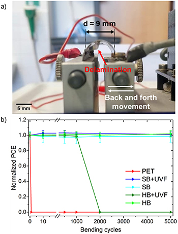
3.3.3. Mechanical stability
A cyclic bending test was applied to solar cells with AgNW bottom electrode fabricated on 2.5 cm × 7.5 cm substrates that are encapsulated either from both sides or from the top side only. The devices fabricated on PET and encapsulated from both sides already delaminate after the very first bending with a radius of ∼4.5 mm, as indicated by the red arrow in figure 6(a). In contrast, devices that are fabricated directly onto barrier films and are encapsulated only from the top side of the devices exhibit higher mechanical stability against cyclic bending. Figure 6(b) plots the PCE of all solar cells during the course of the bending cycle test normalized to their initial values. As already indicated by visual inspection (delaminated devices are horizontally split into two parts between the active layer and the hole-transport layer), the sandwich-encapsulated devices having a total thickness of ∼300 µm instantly stop working already after the first bending. On the other hand, all top-encapsulated devices (85–247 µm thickness) maintain their full performance during the first 1000 bending cycles.
Figure 6. (a) Image of the bending test setup holding a sandwich-encapsulated solar cell under bending conditions with a bending diameter of ∼9 mm. The delamination that is occurring between the substrate and the inner barrier foil after the first bending is indicated by a red arrow. (b) Normalized PCE of AgNW-based solar cells processed on PET and being sandwich-encapsulated from both sides (red) and processed on barrier films (all other colors) and being encapsulated from top side only in the course of 5000 repetitive bending cycles with ∼4.5 mm bending radius.
Download figure:
Standard image High-resolution image
There are two main reasons that lead to mechanically more robust devices. On one hand, the flexural rigidity is decreased because of the reduced total thickness of the devices. The flexural rigidity (D) is given by the following equation [43]:
where E, t, and ν stand for Young's modulus, thickness, and Poisson's ratio, respectively. The proportionality of the flexural rigidity to the third power of the thickness shows that the reduction in thickness significantly improves the device flexibility. This also explains, why the top-only encapsulated devices fabricated on high barrier with UV filter (thickest among all barrier foils) start to delaminate after 1000 bending cycles, whereas devices fabricated on all other barrier films survive the complete bending cycle test (5000 cycles) without any sign of mechanical or electrical degradation.
On the other hand, the origin of the failure during bending is delamination which occurs at the interface with poorest adhesion. As it is also studied by Gregori et al, the weakest interface being susceptible to delamination in such a solar cell stack is between the hydrophobic active layer and the hydrophilic PEDOT:PSS [44, 45]. Our newly developed top-only encapsulated device architecture locates the actual solar cell stack in the center of the device, thereby shifting it closer to the neutral mechanical plane (zero-strain position) in comparison with a standard sandwich-laminated architecture (see figures 2(a) and (b)). The position of the neutral plane, on which zero-strain is exposed, is determined by the Young's moduli and thicknesses of each layer; accordingly, such a symmetrical structure places the zero-strain position close to the sensitive AL/PEDOT:PSS interface, which makes the device mechanically more stable [13].
4. Conclusion
Semitransparent, flexible, fully solution-processed cells with top and bottom AgNW electrodes were fabricated and performed with 5.5% PCE, which is comparable with IMI-based devices. This has been achieved by embedding the AgNW bottom electrode into the ETL layer (AZO NPs) and exposing the cells to 30 min (UV) light soaking, which solved shunting and charge injection/extraction limitation problems. The fact that UV light is necessary for the activation of zinc oxide-based ETLs to be fully functional but also causes enhanced device degradation still remains a problem and emphasizes the importance to develop UV-stable OPV systems and ETLs without UV light-activation necessity.
The developed device architecture comprising AgNW top and bottom electrode enables the manufacturing of cells onto any kind of substrate. This has been demonstrated by fabricating solar cells directly onto different barrier foils, which led to a reduction of the device thickness from 125 to 23 μm and a consequent increase in the specific power from 0.31 to 1.66 W g−1 for devices being fabricated onto the lightest barrier film (32.4 g m−2). Processing cells directly onto barrier foils also resulted in a new encapsulation architecture since such cells require only encapsulation from the top side. This approach yielded significantly thinner and lighter fully encapsulated devices compared to the conventional sandwich encapsulation, showing a superior flexibility and a four-fold improved specific power of 0.38 W g−1. Considering the recent developments of high-performance OPV materials with PCEs >15% (i.e. a factor of three higher) and replacing the top-encapsulation (adhesive + barrier foil) by a printed thin-film barrier, which would further reduce the thickness and weight of the devices by a factor of two, finally suggests industry-relevant OPV with specific power values beyond 2 W g−1 to be realizable in the future.
In conclusion, OPVs with such properties may become superior compared to other PV technologies or even unique for the use in applications that require very high flexibility or maximum power-per-weight ratios, such as textile integration, wearable electronics, or outer space applications.
Acknowledgments
The authors thank Mitsubishi Chemical for providing research samples of barrier foils. The authors also acknowledge the 'Solar Factory of the Future' as part of the Energy Campus Nuremberg (EnCN), which is supported by the Bavarian State Government (FKZ 20.2-3410.5-4-5). The authors also acknowledge funding from the Federal Ministry for Economic Affairs and Climate Action (Project 'OPV4IoT', FKZ 16KN098724) and from the European Union's Horizon 2020 research and innovation program under Grant Agreement No. 952911 ('BOOSTER'). Fruitful discussions within the framework of the European Union's Horizon 2020 research and innovation program under Grant Agreement No. 101007084 ('CITYSOLAR') are acknowledged.
Data availability statement
The data that support the findings of this study are available upon reasonable request from the authors.