

Abstract
This roadmap includes the perspectives and visions of leading researchers in the key areas of flexible and printable electronics. The covered topics are broadly organized by the device technologies (sections 1–9), fabrication techniques (sections 10–12), and design and modeling approaches (sections 13 and 14) essential to the future development of new applications leveraging flexible electronics (FE). The interdisciplinary nature of this field involves everything from fundamental scientific discoveries to engineering challenges; from design and synthesis of new materials via novel device design to modelling and digital manufacturing of integrated systems. As such, this roadmap aims to serve as a resource on the current status and future challenges in the areas covered by the roadmap and to highlight the breadth and wide-ranging opportunities made available by FE technologies.
Export citation and abstract BibTeX RIS
Introduction
Ronald Österbacka1, Tse Nga Ng2 and Xiaojun Guo3
1 Åbo Akademi University
2 University of California San Diego
3 Shanghai Jiao Tong University
Flexible and printed electronics is a highly multidisciplinary research area with the potential for significant breakthroughs in developing new technologies for ubiquitous electronics.
Flexible and Printed Electronics is a multidisciplinary journal publishing cutting-edge research articles on electronics that can be either flexible, plastic, stretchable, conformable, or printed. In this roadmap, we have collected leading scientists' views in various areas related to flexible and printed electronics to give their views on the field. From a scientific viewpoint, we wish to outline the present status, current and future challenges, and what advances in science and technology are required to meet the challenges of flexible and printed electronics to become ready for the market.
The roadmap is divided into three main themes, broadly organized by the main device technologies (sections 1–9), manufacturing (sections 10–12), and systems integration and compact modeling (sections 13 and 14).
Organic light-emitting diodes (OLEDs) and organic photovoltaics (OPVs) discussed by Peng et al in section 1 and Brabec et al in section 2, respectively, are probably the most mature of the different devices covered in this roadmap. Both technologies have seen a steady improvement in performance and reduction in cost over the past years. Stability without proper encapsulation and high material costs are still a significant hurdle when using printing technologies on flexible substrates. In section 3, Chabinyc and Patel present organic thermoelectric (TE) materials and devices as an emerging energy harvesting technology that utilizes heat instead of visible light as a source for energy harvesting.
Thin film transistors (TFTs) are the workhorse devices in display industries, and street in section 4 discusses future directions for this area. Meanwhile, the approach to expand electronic functionalities through heterogeneous integration of silicon and other crystalline materials on flexible substrates is presented by Hussain in section 5. As energy storage is a key component to enable untethered electronics, section 6 by Cobb and Steingart will discuss energy storage devices' requirements and choices for flexible electronic (FE) systems.
In section 7 Torsi et al discuss electronic label-free detection of biomarkers using water-gated organic thin-film transistors (TFTs). The generality of the concept and the promise of single-molecule sensing combined with manufacturing using printing technologies open up new avenues for the early detection of disease. As discussed by Rivnay in section 8, Bioelectronics and E-textiles by Carmichael et al in section 9, are promising avenues for integrating electronic devices with the human body, either internally or externally. These new avenues are still in an early phase of development and will experience different challenges over the next years, but with a very bright future.
For manufacturing, printing tools have steadily progressed to improve feature size resolution, yield, and variability, and the current and future challenges are found in the section by Grau and Subramanian. Aspects of large-area manufacturing using roll-to-roll (R2R) gravure printing of electronic devices are covered by Cho et al in section 11, while in section 12 McAlpine et al discuss the possibilities of using three-dimensional (3D) printing to integrate electronic devices with soft materials into structures with non-trivial form factors, shapes and functions.
In the silicon microelectronics industry, device compact models, process design kits (PDKs), and a robust suite of electronic design automation (EDA) tools enable the efficient design of sophisticated circuits and systems that can be mass-produced by the foundries. In the last decade, research and technology development in the FPE field has formed a solid basis for materials, processing, and devices. How to leverage these technology choices towards making diverse functional systems becomes essential. For that, compact models are needed to accurately describe the devices' electrical characteristics and be incorporated into circuit simulators to perform simulations. A design automation framework to link the FPE technologies and the commercially available EDA tools to perform system simulation and design verification is considered the most critical task. Sections 13 and 14 will discuss the topics of compact modeling and design automation, respectively.
1. Flexible OLED display and lighting
Yuguang Ma1, Dongge Ma1, Junbiao Peng1 and Yong Cao1
1 South China University of Technology
Status
OLEDs can be traced back 70 years ago when A Bernanose et al first observed the electroluminescence (EL) in organic materials, until 40 years later, first practical OLED device was built by Tang et al in 1987 [1]. Flexible OLEDs have been demonstrated as a promising technique for display and lighting applications with smart cell phones as the main application. According to Sigmaintell Consulting, about 470 million OLED panels for cell phones (290 million rigid and 180 million flexible) were shipped in 2019, and significantly grew of 5G mobile phones in 2020 from Digitimes Research. Obviously, flexible OLEDs would act as an important engine in promoting the development of electronic information and lighting.
The production of an OLED screen is a complex process (the optimal selections of light-emitting/electronic and hole injection and transport materials, patterning technologies, backplane technologies, and encapsulation technologies), with the luminescent material in the core. The emergence of novel materials has been pivotal for the development of OLEDs, as shown in figure 1. Fluorescent materials show a low internal quantum efficiency (IQE) of 25% [1], whereas the phosphorescent materials can achieve 100% IQE [2, 3]. Currently, next-generation fluorescent organic materials are being rapidly developed, including thermally-assisted-delayed-fluorescence (TADF) [4], hot exciton [5], and doublet-radical [6] materials. The progress of the blue TADF emitters with anexternal quantum efficiency (EQE) of 20% will greatly promote the display and lighting development. However, these materials are still under investigation and not yet applied in production lines.

Figure 1. Roadmap of OLED emission materials and flexible OLED displays.
Download figure:
Standard image High-resolution imageAt present, flexible OLED displays are mainly fabricated via sublimation in a high vacuum system at a high cost, limiting the area. Therefore, solution-processing has long been anticipated as the manufacturing technology for future OLED displays.
OLEDs will hopefully become the next-generation lighting source due to their unique merits of environment-friendliness, soft light without glare, and flexibility, opening up new markets in the automotive, decorative, and medical sectors [7]. Now, OLED lighting technology is steadily improving, and commercial products with consistent performance in efficiency, lifetime, and colour quality are appearing. For example, the efficiency over 220 lm W−1 was demonstrated in the laboratory in 2020.
Current and future challenges
Although OLED displays and lighting are already in the market and developing fast, as shown in figure 2 [8], challenges remain:

Figure 2. Advances and forecast in efficacy, lifetime, and cost of commercial OLED panels over time.
Download figure:
Standard image High-resolution imageHigh-performance blue EL materials
Low cost and high-performance organic EL materials still need improvement, especially blue light-emitting materials. At present, high efficiency blue phosphorescent materials have operational lifetimes of only a few 1000 h. Therefore, low-efficiency blue light-emitting fluorescent materials are still widely used in the production of OLEDs. While the TADF materials are recognized as potential candidates for higher efficiencies and longer lifetimes, efficiency roll-off at high brightness, as well as the colour purity, still needs to be addressed. There is still significant development needed before materials exhibiting hot-exciton or doublet-radical mechanisms will be applicable.
Simplified OLED device structures
Novel device structures are essential to enhance EL efficacy and stability further, as well as to reduce the costs. To date, complex multilayer structures with high EL performance result in low yields and high costs and simultaneously contribute to the lifetime decrease associated with bending resistance in flexible OLED displays. The enhancement of light out-coupling needs to be solved through optical engineering in order to take full advantage of the flexible display with folding or even arbitrary stretching (figure 1).
Advanced fabrication technology
Owing to the advantages of accurate thickness control and flexible multilayer design, vacuum thermal evaporation is regarded as an effective method for high-quality film fabrication. Therefore, technologies producing high quality, large-area, and patterned films at a low cost that can produce similar quality films are required. However, realizing R2R manufacturing of print layers with the required degree of accuracy is not a trivial task.
Metal oxide backplane technology
Low temperature poly-silicon TFT (LTPS-TFT), so far, is the main driving backplane of OLED displays. This technology is only suitable for small and medium-size utilization due to issues with yield. Although metal oxide TFT (such as Indium Gallium Zinc Oxide) [9] has been used to drive OLED displays with 4K resolution, the electron mobility and photoelectric stability of the TFTs still need improvement.
Advances in science and technology to meet challenges
The efficiency roll-off of blue EL is envisioned to be solved by the design of novel aggregation-induced delayed fluorescence materials. Alternatively, hot exciton materials and high-level charge transfer materials could also provide the solution. Further understanding and control of charge recombination and exciton behavior could provide a chance for high-efficiency materials with a narrow emission spectrum. The low-charge carrier mobility in disordered materials due to the hopping transport of charge carriers and charge trapping leading to degradation are well understood and can be analyzed and modeled to find solutions to help to overcome device degradation.
To improve the bending resistance while reducing the cost of flexible OLED displays, a device with a planar pn heterojunction structure based on an interfacial excimer mechanism with EQE over 10% was realized [10]. Besides, the optical design of the encapsulation may significantly improve the device's light output efficiency. Furthermore, by designing buffer layers to enhance the adhesion between the cathode and organic layer, the bending resistance of flexible OLED devices could be significantly improved. A stretchable OLED device could be realized by developing a stable deformable electrode material.
The inkjet printing technology may solve the bottleneck problem of low-cost, large-area, and patterning, for manufacturing OLED display and lighting, as shown in figure 3. So far, OLED products already are commercially produced in the market with the currently available inkjet printers and materials. Deep understanding ink formulation, droplet jetting and spreading, solvent evaporation, and fusion control is conducive to approve mass manufacturing OLED panels. To challenge higher technology, the electrochemical (EC) polymerization method, which has been successfully demonstrated as a way of fabricating an OLED display with over 1200 pixels, also provides an alternative to producing RGB pixels and high-resolution OLED displays. For fully utilizing R2R manufacturing, printing methods for fully printed cathodes should also be developed.
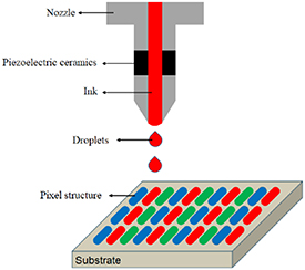
Figure 3. A schematic diagram of inkjet printing OLED displays.
Download figure:
Standard image High-resolution imageThe problems associated with low mobility and instability in the backplanes can be solved using rare earth elements, such as doped oxide TFTs. Right now, the electron mobility of the TFT is over 30 cm2 Vs−1, and the threshold voltage drift is less than 0.5 V under intense white light illumination. This kind of material would be expected to drive large areas and high-resolution OLED displays, even for various types of printing displays.
Concluding remarks
OLED displays and lighting technologies are steadily improving in efficacy, lifetime, and color quality, providing an opportunity for OLEDs in many applications. Although the cost of OLED display and lighting products is higher than LCDs and LEDs, which is also a problem to be addressed, some OLED display and lighting products are available in affordable mobile phones, TV, and automotive lighting applications. To further improve efficiency, lifetime, and reducing the cost of OLEDs, based on the deep understanding of electron excited state processes and carrier transfer/transport process, new light-emitting and matched electron/hole injection and transport materials, novel and simple device structures, advanced and reliably manufacturing, and efficient TFT driving technologies need innovations. With unremitting efforts, the full potential of OLEDs as flexible displays and healthy lighting sources can be unlocked with the help of printing in the future.
Acknowledgments
Funded by the National Natural Science Foundation of China (51521002, 22090024) and the Basic and Applied Basic Research Major Program of Guangdong Province (2019B030302007).
2. OPVs: technology assessment for product development
Christoph J Brabec1,2,3, Andreas Distler3 and Hans-Joachim Egelhaaf1,3
1 Friedrich Alexander Universität (FAU), Material Science, i-MEET,
2 Forschungszentrum Jülich (FZJ), Helmholtz Institut Erlangen-Nürnberg (HI-ERN),
3 ZAE Bayern e.V. Erlangen, Renewable Energies
Status
Photovoltaics (PVs) has become a leading renewable energy technology. Driven by enormous cost degression in silicon PVs, electricity from solar energy is now provided at between 3 and 5 €ct kWh−1 worldwide. Solar technologies are frequently categorized into three generations. Mono- or poly-crystalline silicon solar modules are the first generation, thin film technologies like CdTe, CIGS, etc are the second generation, while the third generation summarizes various emerging semiconductors, among them perovskites, quantum dots, dye-sensitizers as well as organics. OPVs was first implemented in the market in 2008/2009 by Konarka, launching a series of polymer:fullerene (P3HT:PCBM) based solar modules with a nominal peak power between 1 Wp and 40 Wp, depending on size. PVs is typically benchmarked in the key performance indicators (KPI) efficiency, costs and product lifetime. High performance modules from the first and second generation are reaching product module efficiencies of around 20%, a guaranteed lifetime of more than 25 years and costs between 0.3 and 0.5 € Wp−1. OPV modules have a proven record efficiency of 12.6%, a typical product efficiency of 5%–7%. The first generation of OPV modules showed lifetimes of up to 10 years under outdoor conditions and product costs have come down from 10 € Wp−1 and are currently moving towards the 1 € Wp−1 regime. Forecasts anticipating the OPV technology at the GW level are predicting costs as low as 5 €ct Wp−1 [11]. This is the reason why organic modules were designed from the beginning of their product history to complement the classical PV portfolio. Applications such as power plants or roof top integration are of little relevance for OPV as long as the technology is still under development. Therefore, applications that are difficult to access for classical PV technologies are of high relevance (figure 4). These make use of product properties such as transparency, integrability in surfaces, good indoor performance, negligible temperature coefficients, as well as high flexibility and low weight, but also flexible or digital production processes that allow the economic production of small production quantities or single-lot special designs. In summary, a central element of the OPV product roadmap is the design of flexible, colourful and semi-transparent products, which can be integrated into existing structures and fulfil requirements to operate applications with power requirements reaching from µWs up to MWs.

Figure 4. Top: visionary concept of the OPV product portfolio. Flexible, colourful and semi-transparent modules are integrated indoors as well as outdoors into windows, facades, installations, green houses, urban mobility concepts or mobile applications and are becoming part of the daily life, making renewable energies available ubiquitously. Bottom: 'Real World' integration of OPV modules in glass construction elements. Reproduced with permission. (Courtesy Armor SPF GmbH).
Download figure:
Standard image High-resolution imageCurrent and future challenges
Any PV technology must first and foremost meet the classic PV product requirements. Among the classical KPIs, efficiency is probably the most advanced. The current OPV record efficiency is as high as 17.35% on smaller areas and 12.6% on the lab module level and already has surpassed the performance of older technologies like amorphous silicon (a-Si:H) or dye sensitized solar cells (DSSCs) [12]. Device lifetime is increasing quickly. By today, OPV has been proven to be a light stable technology which can operate for tens of thousands of equivalent sun-hours if protected from oxygen and humidity [13, 14]. A more serious challenge is the development of high performance materials which maintain a low bill of materials (BoM). The BoM of the current flexible OPV technology is dominated by the costs for the active material, followed by packaging costs and electrode costs. Semiconductor costs beyond 100 € gr−1 appear prohibitive for mass applications. Few organic semiconductors (OSCs) like P3HT, PCBM, etc already fulfil these requirements, but despite good stability data, their efficiency is a factor 3–5 too low for most products. With non-fullerene acceptors (NFAs), which are considered a most promising material class due to their excellent performance, one must pay more attention to the costs from the beginning. Vacuum processed ultra-barriers as well as inorganic TCO electrodes with costs beyond 10 € m−2 need to be replaced as well.
The most impressive technology feature of OPV is their production by low temperature and low-cost solution coating and printing processes, which offers highest reliability and throughput for such complex architectures as multijunction modules. Nevertheless, commercial OPV products fall short in efficiency compared to record modules processed in the lab (about 5% vs 13%). The consequent reduction of the responsible loss processes when going from lab to fab requires (a) development of semiconductors and semiconductor inks which are fully compatible to environmental and green processing, (b) interface and charge extraction layers forming long time stable contacts, (c) high resolution patterning processes with feature sizes of 100 µm or lower, (d) low cost and high quality lamination and packaging processes which operate below 140 °C.
Advances in science and technology to meet challenges
The product requirements for OPV materials are manifold and include targets for performance, costs, stability, toxicity, recycling, colour, etc. That kind of multi-objective optimization requires a totally different strategy for material optimization, which ideally can be sub-summarized into one figure-of-merit (FoM). Levelized cost of electricity, in its most simplified version, could be such a FoM, as it takes into account the lifetime of modules by balancing the total costs spent over the total energy produced within the lifetime span of the module, where r is the discount rate. One recognizes immediately, that n, the lifetime of the system, is becoming the most influential parameter, which is a major challenge for the R&D community, as the assessment of product lifetime and production costs requires at least the operation of a pilot line and years of outdoor operation.

One alternative option to standardize such combined efficiency, lifetime and costs consideration for the R&D community is the industrial FOM (i-FOM), which was specifically introduced as a more balanced way to report the relevant performance of novel material composites [15, 16]

A central element of the i-FOM is the synthetic complexity (SC), which balances central material parameters like complexity, toxicity, purification etc which all are decisive for the final costs [17]. Figure 5(a) shows the SC as cost equivalent as a function of performance for various polymer-based semiconductors mixed with four difference acceptors. One recognizes that the most efficient material not necessarily is the most promising material for product development. The consequent use of SC and the i-FOM concept is a central strategy to address materials´ related product challenges for OPV and is expected to give valuable guidance, especially to the current generation of NFAs.
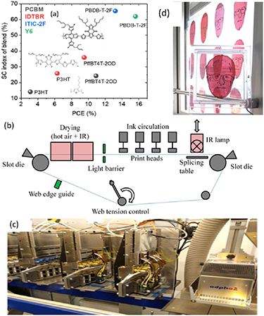
Figure 5. (a) SC for three prototype polymer semiconductors blended with four different acceptors, where PCBM is a fullerene based acceptor and IDTBR, Y6 and ITIC are prototype NFAs. (b), (c) Schematics and image of a loop coater equipped with two slot die heads and 4 × 4 Samba ink jet heads which can produce OPV modules (d) of any shape and form in a single pass up to 172 mm width at 40 m min−1. (b)–(d) Reproduced with permission from (P Maisch, PhD Thesis, Erlangen, 2019.).
Download figure:
Standard image High-resolution imageThe current generation of commercial OPV modules is processed by slot-die coating with shims, which provides lateral resolutions in the mm regime. Laser patterning on roll to roll pilot machines already has been proven to reach a down-web resolution of 100 µms. In order to be able to produce free patterns of solar cells with inconspicuous interconnections, digital printing like R2R ink jet printing is envisaged to become the leading production technology [18]. Ink jet printing also offers the possibility to print OPV directly on objects of discretionary shape, which provides convenient energy supply for Internet-of-Things (IOT) applications.
Concluding remarks
OPV is rapidly progressing towards a PV technology for dedicated applications, which require exceptional aesthetics, integrability and flexibility in design. All these properties are intrinsic to the OPV technology, which is colourful and semi-transparent (due to the excitonic nature), flexible (due to low temperature production on flexible substrates) and aesthetic (due to future digital printing technologies). This positions OPV as a promising technology for indoor as well as outdoor integration on flat as well as curved surfaces, like glasses, windows, shadings or facades. Nevertheless, despite these advantages, OPV has to better address the PV KPIs—especially with respect to costs and lifetime. To categorize materials in terms of an integrative KPI, the i-FOM, is proposed to significantly accelerate the OPV technology and product roadmap.
Acknowledgments
C J B and H J E gratefully acknowledge funding by the Deutsche Forschungsgemeinschaft (DFG, German Research Foundation) under the project numbers 182849149-SFB 953 and INST 90/917, INST 90/1093-1, financial support through the 'Aufbruch Bayern' initiative of the state of Bavaria (EnCN and SFF).
3. Organic TE materials and devices
Michael L Chabinyc1 and Shrayesh N Patel2
1 University of California Santa Barbara
2 Pritzker School of Molecular Engineering, University of Chicago
Status
TEs are based on materials that can interconvert thermal and electrical energy [19]. The efficiency of this interconversion is related to three properties, the electrical conductivity (σ), the thermal conductivity (κ), and the thermopower (S). The FOM at a given temperature (T) is  which is related to the power conversion efficiency of the material. Each of these properties is linked to the charge carrier concentration (n) in a way that makes optimization of ZT is challenging. In TE modules, it is beneficial to use two materials where electron conduction (n-type) dominates in one and hole conduction (p-type) dominates in the other.
Semiconducting polymers were suggested as potential TE materials in the 1980s, but only recently have significant improvements in performance have been obtained due to the advent of new materials and processing routes [20, 21]. Early research on polyacetylene revealed that polymers could have TE performance comparable to inorganic materials [22]. However, the poor stability of polyacetylene in the ambient prevented realization of its promise. The advent of relatively ambient stable conductors, such as PEDOT:PSS, and the wide range of semiconducting polymers (e.g. poly(3-alkylthiophenes)) investigated for thin film electronics has greatly improved the ability to develop organic TEs.
Both p- and n- type organic TE materials have been demonstrated using both polymers and molecular materials (figure 6). The doping process has proved to be a major step in improving TE properties. An impactful approach has been the sequential doping method where a dopant infiltrates a neutral polymer with dopant molecules (either from solution or vapor phase) [23]. The improved TE properties are achieved because the infiltration of the dopant into the polymer matrix maintains the crystalline order, orientation, and long-range chain connectivity permitting high charge carrier mobility. To date, the highest reported power factor ( ) for p-type polymers is ≈350 µWm−1K−2 for PEDOT-Toslylate and doped selenium-substitute diketopyrrolopyrrole polymers [24, 25]. The ZT of these polymers is ≈0.25 based on the thermal conductivities reported in each with a ZT of >0.5 considered important for practical applications.
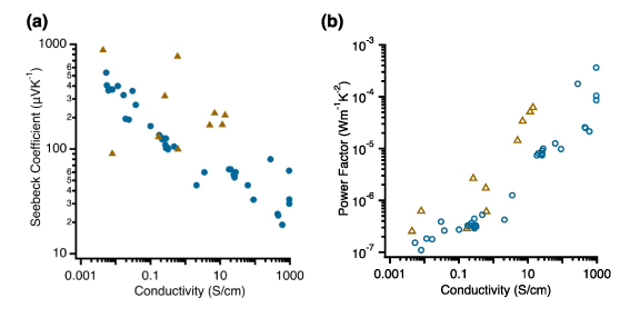
Figure 6. (a) Seebeck coefficient and (b) power factor of homogeneous semiconducting polymers as a function of the electrical conductivity for p-type (circles) and n-type (triangles). Data from literature and tables in [19–24].
Download figure:
Standard image High-resolution imageOrganic TE materials can be integrated into lightweight modules for use in energy harvesting and local temperature control [20]. Importantly, the intrinsic processability of organic materials permits the fabrication of flexible and conformable TE modules based on unique architectures (e.g. corrugated) that go beyond the rigid, parallel plate configuration. Such architectures enable unique opportunities in implementation such as powering wearable electronics and sensors.
Current and future challenges
Electrically doped semiconducting polymers must be resilient to elevated temperatures to push the limits beyond near room temperature applications. The stability depends on both the doping method and polymer itself. For example, polythiophene derivatives with polar side chains of oligo(ethylene oxide) have shown marked improvements in thermal stability in air compared to the nonpolar side chain equivalent. The stability of dopants can be improved through routes such as ion-exchange of charge transfer dopants with more stable counterions [26] and new molecular architectures through so-called 'self-doped' polymers where sidechains are based on ionic pendant groups.
Currently, n-type polymers do not have the same TE performance as p-type polymers. The current best n-type organic polymers have PF ≈25 µWm−1K−2 with the highest values from an organometallic poly(Ni-ethenetetrathiolate) with ≈450 µWm−1K−2 [20, 27]. The origin of this difference is not well-understood given that the electron mobility of many polymers and small molecules is within a small factor of the best hole mobilities. It is possible that the difference is due to a combination of factors such as the design of compatible dopants with high mobility materials, or issues with defects in the materials because of their stability in ambient conditions. Surprisingly, figure 6 shows that although the absolute performance of n-type material is less than that of p-type materials, the power factor at a given electrical conductivity is higher for n-type polymers.
Another factor that is not well-understood is the trade-off between electrical conductivity and thermal conductivity in organic materials. The thermal conductivity of insulting polymers is still not easily modelled due to structural disorder [21]. The anisotropic molecular packing in organic materials further makes it difficult to relate the thermal and electrical conductivity. Developing new methods that are tailored for the measurement of anisotropic thermal conductivity of OCSs will be needed. Because organic TEs are very close to practical levels of performance, accurate assessment of the thermal conductivity will be a decisive factor in their utility.
Advances in science and technology to meet challenges
Improvements in models for charge transport and thermopower of OSCs will greatly enhance the ability to determine design rules for organic materials. There has been significant progress developing models to understand the connection between the thermopower and the electrical conductivity of homogeneous materials [28]. Strategies to tune the electronic density of states (DOSs) in blends towards higher thermopower have been reported and corroborated experimentally [29]. If such models are coupled with similar advances in models for thermal transport, it will accelerate the ability to improve the performance of materials.
New architectures for TE modules that leverage the unique features of OSCs, such as their ability to be printed or extruded by additive manufacturing (AM) methods, will provide a pathway to realize their performance [20]. Coupling designs of modules that leverage the anisotropies in the electronic and thermal conduction of polymers could provide further advances. The ability to spatially tailor transport properties (i.e. functionally graded materials) across the length of the organic materials, such as formation of dopant gradients and microstructure, is potentially simpler than in inorganic materials and is ripe for exploration [30]. Such an approach can enable improved distribution of heat when operating TE modules as Peltier coolers.
Concluding remarks
OSCs are close the level of performance that are required for practical applications in energy harvesting and temperature control. Pathways to ZT > 0.5 seem achievable for p-type polymers and it is likely that n-type polymers can also achieve similar or even higher performance. If new materials pairs that are readily processable are developed, then we can expect to see greater exploration in module designs that leverage the unique properties of semiconducting polymers.
Acknowledgments
M L C acknowledges support from NSF DMR 1808622.
4. Printed or flexible TFTs; materials and performance
Robert A Street1
1 Palo Alto Research Center
Status
OSCs dominate research on printed TFTs and since 1985 their mobility has increased from 10−5 cm2 Vs−1 to about 10 cm2 Vs−1 (see figure 7) [31, 32]. The improvement resulted from the discovery of new OSCs, particularly the donor–acceptor polymers. Small molecules tend to have higher mobility than polymers, although many cannot be deposited from solution. The mobility and other TFT characteristics depend on the choice of gate dielectric and the method of fabrication. Organic TFTs are readily made flexible by deposition on a wide range of plastic substrates. Instability to a gate bias voltage and ambient humidity was a constant issue with organic TFTs, but has substantially improved [33].

Figure 7. Organic TFT mobility trend over 3 decades, showing the typical range of values for p-type and n-type devices [31].
Download figure:
Standard image High-resolution imageFlexible inorganic TFTs are in production for liquid crystal displays, organic light emitting displays and x-ray detectors—amorphous silicon (a-Si), LTPS made by laser recrystallization and metal oxides, primarily InGaZnO (IGZO). Backplanes are fabricated on a thin polyimide film released from a glass carrier after processing, giving equivalent TFT performance to those deposited on glass. A-Si and IGZO can be deposited below 200 °C with minor reduction in performance making them accessible to other plastic substrates [34], and IGZO can be printed from a sol-gel solution with annealing at about 400 °C. IGZO flexible microprocessors have been demonstrated [35].
Printed and flexible TFT materials outside the above categories include the perovskites developed for solar cells, carbon nanotubes (CNT), graphene and other two-dimensional (2D) materials, each of which show promising TFT properties [36]. Electrolyte gated and EC TFTs use a liquid or solid electrolyte gate dielectric and operate by transferring charge from the gate dielectric directly to the semiconductor, often PEDOT. ECTFTs typically have high current but slow response and have applications for chemical sensing [37].
Printed TFTs are largely targeted at IoT devices, small and possibly disposable flexible tags with an internet link. Such applications could increase enormously if advanced by a robust printing and TFT material technology. Concerns about stability and process integration have so far prevented printed TFTs from reaching the display backplane market.
Current and future challenges
Numerous printed organic TFT device prototypes are reported but have not yet reached significant manufacturing production, although there is early stage manufacturing of non-printed organic TFTs. Technology adoption is held back by issues of uniformity and process integration as well as device performance limitations of mobility and speed as compared to inorganic TFTs. Many of the TFTs shown in figure 7 are made with Si/SiO2 gate dielectric but have lower mobility when made with a solution-deposited dielectric on a flexible substrate.
Printed TFTs have the additional challenges of print resolution, parasitic capacitance and process integration. Ink-jet printing is an attractive method because it is a digital technology. However, commercial ink-jet printers have a printed feature size of 40–50 µm, while large area lithography has feature size down to 1–3 µm. Comparable printed features are possible but not yet with high throughput scalable commercial systems [38]. Large TFTs take up space and have high parasitic capacitance, which reduces circuit performance compared to lithographically defined devices. The challenge is to reduce the disparity in feature size to make printed TFTs competitive with lithography. Printing systems must print all the various materials used in the TFT and obtaining a thin uniform defect-free gate dielectric is particularly challenging.
Hybrid circuits (figure 8) are developed to solve some of the performance limitations [39]. Printed devices provide the simple circuit elements and silicon integrated circuits (ICs) provide the capability for complex processing, data storage and wireless communication. The problem is that the IC could contain virtually all the necessary devices so that few printed TFTs are needed. The challenge for TFT technology is to be capable of sufficiently complex circuits that minimize and eventually remove the need for ICs. The challenge for ICs is to be thin, flexible and bondable to plastic substrates.
Figure 8. Printed light and temperature wireless sensor, as an example of hybrid flexible electronics, with some printed TFT circuits, some conventional components and printed silver interconnects. © [2017] IEEE. Reprinted, with permission, from [39].
Download figure:
Standard image High-resolution imageInherently large circuits such as displays, and devices such as TFT sensors, high voltage or ferroelectric TFTs, as well as other characteristics such as stretchability or transparency, may provide opportunities that only printed or FEs can meet. The challenge is to find applications of this type and to develop new devices to satisfy the need.
Advances in science and technology to meet challenges
The ideal printed or flexible TFT has high mobility, high on/off ratio, sharp turn-on, small features with precise dimensions, is self-aligned with a high k gate dielectric, and is stable against electrical stress and ambient exposure. There is broad scope for continued development of materials to achieve these goals. Continued improvement in OSCs with higher mobility and increased stability against ambient exposure and bias stress is a reasonable expectation. Development of printable metal oxides including p-type materials, that can be processed at low temperature with stability and high mobility would open up new device opportunities. Novel TFT materials including graphene, CNT and transition metal dichalcogenides, show promise but need research to develop them into robust printed TFT technologies. Important for these materials is to find the combination of semiconductor and gate dielectric that give high performance.
The printing process needs further research to achieve higher density devices with faster circuit speed, both of which are limited by printer resolution and precision. Printed feature size should decrease to 5 μm or below in high throughput systems, and feature overlaps to 2 μm with corresponding alignment accuracy between layers. Self-aligned processes are desired as the parasitic TFT capacitance limits the circuit frequency. There are printing techniques that are capable of high resolution, such as gravure, extrusion and nano-imprint technology, but need further research to demonstrate process integration of the TFT devices and circuits. Printers should be enabled for the multiple materials that are used in devices. As feature sizes reduce, the problems of the liquid/surface interactions increase and will need more research into wetting, inter-diffusion and other surface interactions. Since printed TFTs will have limited resolution for the foreseeable future, 3D integration can help achieve high density circuits. Initial progress in 3D integration needs to be developed into a robust technology [40].
Vacuum deposited and lithographically patterned flexible a-Si, LTPS and oxide TFTs are in volume production and so their research advances are directed to new application spaces. Oxide TFTs are limited in their use for backplane drivers by the lack of good p-type materials for complementary circuits, which is an important gap to fill.
Concluding remarks
Printed TFTs have progressed greatly but still fall short of being a robust manufacturing technology. There is a wide variety of materials, devices, circuits and processing approaches that have been demonstrated at the prototype stage for printed and/or flexible systems. Future research and development will determine which of these approaches come together to form a successful manufacturing ecosystem, capable of addressing novel applications and competing with conventional approaches.
5. Flexible silicon electronics
Muhammad M Hussain1
1 KAUST and UC Berkeley
Status
FEs is an emerging area which potentially will obliterate the interfacing barrier between readily available physically rigid electronic components and natural biology which have asymmetric surfaces, irregular architecture, soft and textured 'components'. Such electronics will allow us to interface seamlessly with natural biology (human, animals, plants, etc.). That will help us to understand natural phenomena deeply and to reapply them in our daily life through nature-inspired engineering. Since 2000, substantial progress has been made in the general area of FEs [41]. This drive is influenced by innovation in materials. Since polymers are naturally flexible there has been noteworthy attention toward polymer-based electronics. In parallel, 1-dimensional (1D) materials (such as CNTs and nanowires), as well as 2D materials (such as graphene and two dimensional dichalcogenide materials) are all ultra-thin and thus, naturally flexible. Another approach has been to use zero-dimensional materials (organic materials) and some of the aforementioned materials as 'ink' in inkjet-printed texturing and/or 3D printed shaping. Undoubtedly, major progress has been made in using these materials for FEs. Nonetheless, one critical challenge remains unaddressed. Although the aforementioned materials show exciting potential for a variety of applications, for data management their efficacy remains questionable and not competitive to existing traditional electronic materials such as mono-crystalline silicon which is used to make 90% of the electronics today [42]. Before we proceed, let us first address what is data management. Data management includes data processing, data storage and data transmission. Since any electronic system focusing on the IoT or Internet of Everything involves sensors, it is obvious that gathered data through the sensors has to be managed properly. Although widely used crystalline thin films like silicon, silicon germanium, germanium, III–V, gallium nitride, silicon carbide, etc are essential today for data management electronics (such as logic microprocessor, memory and transceiver), optoelectronics, power electronics, etc, they are physically rigid and brittle. Therefore, nearly no attention was paid to these materials irrespective of their reliability, manufacturability, and functionality. The idea has been to use them as they are but that contradicts the vision of a fully FE system.
Current and future challenges
Today, flexible hybrid electronics (FHE) is a popular term in the scholarly community working in the general area of FE [43]. The concept is to continue using traditionally rigid ICs because they are small, readily available, and cheap. In reality, none of these is entirely true. Additionally, it is contradictory to the vision of a fully FE system. But, why do we even need a fully FE system? To address this, as an example, one of the most prized objectives for the FE community is to develop an implantable brain–machine interface that can be placed in the intracranial space on soft matters of the human brain to maximize its interaction. The concept expands further that such a system will be able to transmit data even when the scalp is closed. However, not a single demonstration as of today eliminates the necessity of the physically rigid data management ICs [44, 45]. On occasions, it has been recommended to use serial ports to interface between the sensor array and the accessorial I/O interfacial electronics. The question is why these challenges still exist? The truth is lack of appetite to use physically rigid traditional electronic materials due to their lack of novelty in curiosity driven academic research has made it a show stopper to begin with. Next, the complexity related to their processing using complementary metal oxide semiconductor (CMOS) has been left with semiconductor industries who sporadically showed its promise but due to absence of clearly profiting ventures never picked it up seriously. Additionally, absence of sophisticated equipment in the academic environment also played a negative role. To achieve a fully FE system even with only the data management electronics as flexible silicon electronics, major obstacles have to be overcome: thinning down the silicon-based bare die containing the transistors and other electron devices; their reliable transfer to the soft encapsulation materials; placement and attachment; interconnection, etc are a few to name. While some demonstrations address a few of these, rarely all have been addressed in a comprehensive manner.
Advances in science and technology to meet challenges
Initially, silicon-on-insulator (SOI) substrates were used to remove the buffer oxide layer conveniently to release the top SOI layer for FE materials. However, some critical show stoppers nearly halted its progress: expense and lack of proper device isolation strategy for ultra-thin (3–150 nm) flexible SOI layer [42]. Another approach capitalized on using silicon (111) substrate is due to higher atomic density, it is difficult to etch crystalline plane (111) while it is relatively easy to etch vertical plane (100). Unfortunately, due to high defect density, (111) plane is not recommended for any data management electron device [42]. Next approach has been to create a porous network in bulk silicon substrate using anodic etching followed by expensive epitaxial growth of silicon before peeling it off using the already formed porosity. Expense and low throughput have obstructed its progress [42]. Another approach has been to use abrasive back grinding or lapping/polishing to reduce the material from the back side of silicon substrate. Not only it is physically damaging, it also has limited removal ability, leaving the left over silicon not reasonably flexible. Also, some of the processes are expensive specially considering they remove a significant portion of the substrates. This ultimately compromises device performance such as PV efficiency of crystalline silicon solar cells [42]. Finally, controlled cracking in the substrate using a metallic layer has been demonstrated which suffers from the loss of any free hanging micro-electro-mechanical systems (MEMS) devices in the back end of line processes. Additionally they are complex and expensive [42]. Since, none of these processes has shown a full blown pragmatic prospect, only three entities have made substantial progress. Belgium based imec has shown a variety of encapsulation techniques for ultra-thin silicon but they have never been able to demonstrate a full system [46]. USA based American Semiconductor sells some useful chips like microprocessors and analog-to-digital converter, but again they also have not shown a full system [47]. We are the only group who have shown a 3D architecture for fully functioning physically flexible standalone electronic system integrating sensors, actuators, power supply/storage and data management electronics (figures 9 and 10) [48–50].

Figure 9. In this schematic (left to right and top to bottom), a highly manufacturable heterogeneous integration strategy is demonstrated for achieving a flexible silicon electronic system. Initially a soft material temporary host site is adopted followed by polyimide deposition. Next patterning is done where each pattern is curved in a way to match the shape and size of the incoming flexible silicon ICs. Then, an interconnect metal layer is deposited followed by patterning. On separate locations, logic/memory, radio frequency (RF) IC and battery are curved with certain shapes and sizes to provide them with some unique identities. Then they are transferred to the temporary host sites and their placement (dubbed as Lego like Pick and Place Assembly) is done (like DNA assembly, each component will fit only in designated location due to the curved pattern in the host site and the unique identities formed in the ICs). Polydimethylsiloxane (PDMS) is formed and etched back to reduce its thickness much lower than the ICs. ICs are now etched back with reactive ion etching (RIE). Next another layer of PDMS is formed with patterning to reach out to the underlying thinned downed ICs. Metal layer is deposited followed by patterning to curve out antennas and free space for placing the solar cells facing upward. Another layer of PDMS is formed and patterned to conduct corrugation enabling etching to curve an alternate pattern in the solar cells to make them flexible. Release the flexible system from the temporary host site, flip it to expose the sensors with the data management electronics and battery embedded in the middle of the soft encapsulation layers (placing them in the neutral plane) while exposing the antenna and the solar cells on the other side of this coin like 3D architecture. (M M Hussain and S F Shaikh, 'HETEROGENOUS INTEGRATION OF PLURAL GRAPHENE SENSORS ON 3D COIN CMOS ELECTRONICS,' PCT/IB2020/051141, 2019.).
Download figure:
Standard image High-resolution image
Figure 10. A fully flexible standalone integrated silicon electronic system with microprocessor, memory, BLE transceiver, antenna, an array of micro lithium ion batteries, solar cells and sensors with light actuator.
Download figure:
Standard image High-resolution imageConcluding remarks
As much as FEs offer exciting promise, unless we have heterogeneous integration strategies of hybrid sets of materials to develop manufacturing grade fully flexible standalone electronic systems, its promising potential will not be fully realized. Adopting some generic integration sequence, as we have developed and demonstrated, will allow the user and the developer community to project some highly profiting applications for immediate use by consumers. Also, some niche areas need to be identified focusing on industries who are not traditionally using electronics in their products due to their existing rigidity and bulkiness. Finally, comprehensive analytical studies need to be conducted to validate each material and process to ensure that the perceived FEs will not compromise the advantages offered by their rigid counterparts. For absolutely novel wearable and implantable applications, it will be critical to retain their performance and reliability in context of uncertainty posed by user behavior.
Acknowledgments
The author acknowledge many students, post docs and research staffs who have worked on projects involving FEs. The authors also acknowledge a variety of funding sources.
6. Energy storage
Corie L Cobb1 and Daniel A Steingart2
1 University of Washington, Seattle, WA, United States of America
2 Columbia University, New York, NY, United States of America
Status
Energy storage materials are critical to enabling untethered FE devices. Wearables and smart devices that incorporate FE are equipped with a range of sensors and circuits for wireless communication and place new power, energy, lifetime, and mechanical durability demands on energy storage materials. In this brief review, we will consider advances and challenges in closed-form capacitive and EC storage (e.g. capacitors and batteries) as well as open-form EC storage (e.g. fuel cells). Specifically, not addressed in this review are thermal and mechanical storage mechanisms as these storage technologies are greatly limited in applications with large surface to volume ratios, which encompasses all flexible technologies. Recently, significant advances have occurred in energy storage for FE with the emergence of new nanomaterials and composite structures [51], fabric and wire-shaped device formfactors [52, 53], and more robust mechanical integration [54].
A capacitor is a passive electronic component that stores energy through separation of charged species for short durations. A battery converts chemical energy into electrical energy by means of an EC oxidation-reduction reaction and is traditionally optimized for power or energy density. Existing energy storage materials and mechanisms that will be used for flexible form factors are inherently the same, but FE devices require the development of new passive materials for electrical conductivity, ionic conductivity and mechanical integrity, as well as modified manufacturing methods and end-product packaging. Batteries in particular are 30% or more of a device's volume in many wearable and portable devices on the market today [55] and will likely increase in this fraction. Energy storage materials must have sufficient energy and power to enable untethered device operation while sustaining various modes of mechanical deformation at high strain rates. Figure 11 summarizes the current state of the art.

Figure 11. Ragone plot of energy storage technologies for flexible electronics applications.
Download figure:
Standard image High-resolution imageAfter nearly 20 years of R&D, a key question remains for the FE designer: to harvest or not to harvest [56]. A highlight is PV technology used in combination with batteries which has shown promise for two decades and continues to be the most reliable combination for harvesting and storage [53] as the areal requirements for power input and the volumetric requirement for energy storage are complementary. Conventional silicon-based PV cells use brittle planar substrates which limits applicability to FE. Dye-sensitized solar cells (DSSCs) and OPVs are two promising technologies that break the barriers of traditional solar technology and enable flexible substrates with R2R manufacturing capabilities (see section 2). DSSCs and OPVs have efficiency limitations and alone cannot supply the necessary energy required for FE.
Micro-scale fuel cells have been considered as a potential battery replacement and can be recharged instantaneously through the addition of additional fuel sources. However, the overhead of fuel delivery and management make these devices challenging for integration with FE applications. This said, fully replaceable batteries that are disposable with the device (e.g. actively functional bandages) may benefit from a metal-air primary battery, a mechanically simpler cousin to fuel cells.
Current and future challenges
Significant progress has been made over the last decade with the development of a wide range of promising energy storage materials. However, developing more robust and flexible manufacturing and packaging solutions for energy storage materials remains a grand challenge. Fabrication and integration of high performance and compact power and energy sources with high flexibility, stretchability and conformability is critical to advancing FE. Packaging is integral to protecting batteries, capacitors, solar cells, and microfuel cells from the external environment, however most solutions available today do not seamlessly integrate with many FE applications. Packaging deals with a conflicting set of design requirements; packaging must be mechanically compliant while protecting materials from the external environment with sufficient safety and mechanical durability. Focusing on batteries, integrating metal current collectors, brittle electrodes, separator sheets, electrolyte, and packaging while maintaining desirable mechanical properties is one of the most significant barriers to commercializing high performance batteries for FE. Progress in packaging and integrating Lithium-ion solid-state battery components has been made as demonstrated in work by Chen et al [57], but further testing and research is needed to understand longer-term durability beyond 100% strain. Focusing on stretchable and flexible formfactors, Gaikwad et al [52] demonstrated a flexible, printed alkaline battery based on a mesh‐embedded architecture, as shown in figures 12(e)-(b), while Kwon et al [58] showed the potential of a cable-type Lithium-ion battery architecture that could be used as a conformal fiber. To maximize the 'F' in FE energy storage, the field must move away from traditional bulky stacks of materials in metals cans and vacuum sealed pouches. New conformal manufacturing methods, device architectures and novel packaging techniques will be key to advancing the field and eventual product commercialization.

Figure 12. (a) Future AM vision for manufacturing flexible and portable electronic devices. Characterization of a flexible printed battery with an active footprint area of 3.2 cm2 is shown in (b)–(e). (b) Discharge profile of the flexible battery when discharged at 0.5, 1, and 2 mA when flat. (c) Discharge profile of the flexible battery when flexed to different radii of curvature while discharging. Discharge experiments were carried out at 1 mA. (d) Demonstration of two flexible cells connected in series to power a green LED. (e) The flexible batteries connected in series were able to power the green LED when flexed to a bend radius of 0.3 cm. (a) is reproduced from [55] (Copyright 2016 by The Electrochemical Society), and (b)–(e) are reproduced from [52] John Wiley & Sons. (Copyright 2011 WILEY‐VCH Verlag GmbH & Co. KGaA, Weinheim).
Download figure:
Standard image High-resolution imageAdvances in science and technology to meet challenges
Developing new devices requires developing new scalable fabrication methods to make them and new characterization methods to quantify their performance. Whether batteries, capacitors, microfuel cells, or solar cells emerge as the dominant storage technologies for FE, the field must move away from batch-scale processing and develop more consistent testing standards. As mentioned previously, established EC couples can be used as model systems, and FE power source development can and should focus on ancillary systems and manufacturing.
AM has been available to designer since the 1980s, but has gained attention as a fabrication pathway for FE electrode and cell architectures with increasing precision and lower pricing of automation. In the context of energy storage, the freeform fabrication capabilities of AM coupled with its capability to print a wide range of materials, makes AM a leading candidate for creating highly integrated FE devices as shown in figure 12 [55]. To highlight a recent example, Zhang et al demonstrated the impact of inkjet printing and extrusion to fabricate all-MXene-printed structures for micro-supercapacitors [59]. As the authors point out, surfactants and additives, which are typically involved in formulations, adds complexity to creating AM-compatible ink solutions and reduce printing resolution. In addition, Kumar et al [60] used screen printing to fabricate a Zn‐Ag2O rechargeable battery with high reversible capacity and discharge current density under 100% stretching loads. This achievement was enabled by a new conductive ink formulation with a highly elastic binder. While we highlight inkjet and screen printing technologies here, 3D printing and other R2R-compatible deposition technologies are also applicable and are discussed further in sections 11 and 12. AM also enables the fabrication of novel electrode and cell architectures [55] which can be engineered to withstand high strain loads while delivering high energy and power relative to conventional planar material stacks. Typically, increases in power density are only possible through sacrifices in energy density where thin electrodes and low mass loading (<1 mg cm−2) are employed. Engineered electrode architectures can break these trade-offs, especially in EC systems [61]. As the field moves towards commercial-scale applications, AM will be integral to scaling up FE energy storage. Note that many of these achievements are demonstrated with air and water stable systems as a proof-of-concept: there is no reason they cannot be applied to air-sensitive chemistries, as discussed by Hager et al in a recent article on polymer-based systems [62].
FE energy storage devices are subjected to more demanding mechanical modes of deformation than traditional stationary applications. Standardized and quantitative evaluation of the mechanical durability of energy storage technologies is needed for longer-term commercialization of the technology. Most mechanical tests conducted to date are qualitative and follow loose forms of conventional ASTM testing standards. Further research into standardized mechanical tests and apparatuses to better measure flexibility, stretching and other modes of mechanical deformation is needed by the field.
Concluding remarks
Energy storage solutions require higher power and energy in thin, durable and cost-effective form factors that can withstand the dynamics of human movement and harsh environments. The field also needs more systematic design criteria for selecting electrode–electrolyte materials and quantifying their mechanical performance once integrated in a device. Given the advances made for today's electric vehicles, smartphones, and other consumer electronics, FE can make similar strides in energy storage over the next 10–20 years to better meet current and future demands for high power and energy device operation if the critical needs discussed in this section are more rapidly addressed. Energy storage integration with FE devices will be the key to advancing the field and commercializing more seamless wearable and portable devices. AM is a revolutionary fabrication pathway that can open new scalable approaches for on-demand fabrication of flexible and stretchable, shape-conformable FE energy storage technologies.
Acknowledgments
C L Cobb acknowledges that this work was funded in part by a Defense Advanced Research Projects Agency (DARPA) Young Faculty Award under Grant No. D19AP00038. The views, opinions, and/or findings expressed are those of the authors and should not be interpreted as representing the official views or policies of the Department of Defense or the U.S. Government.
7. Large-area printable and FE biosensors for label-free single-molecule detection
Luisa Torsi1 and Ronald Österbacka2
1 Università degli Studi di Bari
2 Åbo Akademi University
Status
Field-effect transistor-based biosensors have been extensively developed over the past 30 years [63]. Label-free electronic transduction is perceived to be conveniently fast and wieldy. The general strategy to bio-sensing involve a transducing interface functionalised with biological recognition elements, such as antibodies or DNA probes, that endow the device with recognition properties by selectively capturing the analyte, e.g. an antigen or a genomic marker, respectively.
Detecting a biomarker or a pathogen at the physical limit is the new frontier in medical analysis as it endows the clinicians with the attacker's advantage over life-threatening diseases such as tumors and pandemics. Within this field, two main classes of transducing approaches are pursued. One approach to single-molecule electronic label-free transducers, schematically featured in figure 13(a) involves a nanometric interface hosting few recognition elements. The second approach, suitable for printed electronics manufacturing, involves a much more extensive interface hosting trillions of highly packed bio-recognition elements (figure 13(b)).
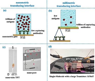
Figure 13. Nanometric vs large-area millimetric transducing interfaces. In panel (a) the case of a nanometric gate hosting just a few capturing antibodies while in panel (b) a large gate hosting 1012 is featured. In panel (c)-left the single carbon nanotube thin-film transistor is shown (Reprinted with permission from [64] Copyright 2011 Springer Nature), while in panel (c)-right the cross-sectional sketch featuring a nanopore system through which charged single-molecule translocate (Reprinted with permission from [65] Copyright 2012 Springer Nature). In panel (d) a picture of the Single-Molecule with a large Transistor (SiMoT) device is provided.
Download figure:
Standard image High-resolution imageIn the former case, the probability for an analyte to impinge on the nanometric interface is unfeasibly low, unless the analyte molecules are present at a concentration in the nanomolar (10−9 mole l−1) range or higher [66]. An example of an electronic transducing nano-interface is provided by a CNT field-effect-transistor (FET) detecting a single copy of a DNA biomarker (figure 13(c)-left). The nanotube bears few single-stranded DNA probes complementary to the analyte covalently attached to a point defect. Relevantly, the concentration of the genomic analyte is in the μM range [64]. This concentration assures that in 100 μl there are 1014 analytes available for the binding to the few probes attached at the nanometric interface. At the same time, statistically, there is one analyte molecule in each sub-volume with an edge of 100 nm. Hence, wherever the detecting nano-interface falls in the solution volume, there is always an analyte ready for the interaction. A similar approach is undertaken in the system shown in figure 13(c)-right were charged biomarkers at a concentration of 50–100 nm can go, one-by-one, through a nanopore generating transient blockades in the trans-pore current [65]. While this approach enables one to study rarer interactions that would be lost in an ensemble measurement, it cannot address detections at a single molecule in a large sampling volume.
Current and future challenges
The challenge in the field of biosensing is ultimately to be able measure one single molecule in a large volume such as 100 μl. This challenge means being able to deploy a technology that can detect 10–20 × 10−21 mole l−1 (zeptomolar). The preferred approach to label-free single-molecule electronic sensing (figure 13(b)), involves a large millimetre-wide interface that hosts as many as trillions recognition elements that are, hence, highly packed [67–70]. By placing 104 capturing proteins per μm2 to the surface of a sensor, the protein packing resembles the receptors on a cell surface. Interestingly, cells, which are by no mean nanometric objects, can perform single molecule tracking and detection [66]. Therefore, 'Single-Molecule with a large Transistor (SiMoT) technology' was proposed [71, 72] to mimic the behavior of cells when sensing markers at extremely low concentrations in solution. A picture of one of the prototypes of a SiMoT device is provided in figure 13(d). It is based on an electrolyte gated organic FET [68, 69] operated in deionised water, with a gate that has an area of ca. 0.5 cm2, hosting 1012 antibodies or genomic probes. The SiMoT platform has been proven to perform label-free and selective detection at the physical limit in real biofluids of protein biomarkers such as human Immunoglobulin G, Immunoglobulin M, C-reactive protein, MUC1 and HIV1 p24 antigen as well as genomic markers such as miR-182-5p and KRAS. Indeed, the widely applicable method used to conjugate the recognition elements to the gate electrode, makes the SiMoT platform suitable for the detection of different classes of markers and pathogens reaching record detections limits for label-free protein detection.
The SiMoT sensing gate is enormous compared to the molecule to be detected, and the future challenge is to rationalise how this is possible at all. It is like spotting the wave generated by a single-droplet of water falling on the surface of a 1 km squared lake. The model developed so far foresees that an amplification effect takes place, associated with a hydrogen-bonding network that connects the recognition elements. The model well reproduces some of the experimental results, but still, there is the need for an all-around experimental proof for the proposed mechanism.
Advances in science and technology to meet challenges
At this stage, besides deepening the knowledge of the fundamental aspects underpinning the sensing phenomenon, the field of biosensing needs to produce more sophisticated technologies that can be manufactured in quantities. To this end, more work on the design, development and fabrication of bio-electronic systems that can perform ultra-sensitive detection of both proteins and DNA biomarkers needs to be done. In order for this to be feasible, lab-based devices need to be translated into cost-effective portable multiplexing arrays with fast time-to-results. We foresee a structure that resembles that of a 96-well Enzyme-Linked ImmunoSorbent Assay (ELISA) plate, but is all electronic, much more sensitive and label-free. One such example is schematically featured in figure 14. The complete system is based on large-area compatible solution-processed bio-electronic sensors fabricated on a flexible substrate, connected using printed electronics to a silicon IC interface which amplifies, digitalises and sends the signals to a computer via USB (https://simbit-h2020.eu).

Figure 14. The main features of the SiMBiT (https://simbit-h2020.eu) system. Reproduced with permission from (https://simbit-h2020.eu).
Download figure:
Standard image High-resolution imageDigitising biomarker analysis by detecting down to the single-molecule level is the new frontline for expanding the knowledge in the booming field of precision health. Such an incidence will enormously enhance clinician's ability to cure diseases by enabling better prognosis and allowing the implementation of precise treatment methods. We foresee substantial progress in the quality-of-life of the population for generations to come, along with a decrease in health-care expenses.
Concluding remarks
Single-molecule detection is a new paradigm in ultrasensitive biomarker and pathogen detection. Combined with an electronic, label-free detection it holds the potential to revolutionise our current approach to biosensing. Indeed, large-area interfaces crowded with trillions of recognition elements capturing either a protein or a genomic marker have shown record performance level even in real biofluids. We foresee that novel bio-electronic smart systems, will open up a significant use of high-throughput array-based assays, not only in clinical laboratory analysis but also in point-of-care and low resources settings.
Acknowledgments
We acknowledge Irene Esposito, Fabrizio Torricelli, Eugenio Cantatore, Guillaume Fichet, Pietro Larizza and Fabien Marty for useful discussions. The H2020—Electronic Smart Systems—SiMBiT: Single-molecule bio-electronic smart system array for clinical testing (Grant No. 824946), Academy of Finland projects #316881 and #316883, and the Åbo Akademi University Endowment through the CoE in ''Bioelectronic activation of cells" are acknowledged for financial support.
8. Bioelectronics
Jonathan Rivnay1
1 Northwestern University
Status
Bioelectronics describes the interfacing of engineered (opto)electronic components and devices with biological systems. While early persistent success in bioelectronics was limited to neural and cardiac pacing, or point of care approaches for measuring one or two analytes (i.e. blood glucose), the field has grown to leverage recent advances in materials, fabrication, and medicine. Bioelectronics remains broad in scope with performance metrics and design needs strongly dependent on applications. Such needs depend on a wealth of factors: in vitro vs. wearable vs. implantable, acute vs. chronic, mode of action. Often devices meant to interface with living organisms are developed as either advanced tools for biological discovery via research on animal models (fundamental research), or as bioelectronic tools for human health.
Recent efforts in bioelectronics have focused on device form factor, resulting in ultra-light, conformal or miniaturized devices, leveraging new developments in materials processing and fabrication (figures 15(a) and (b)) [73, 74]. New materials have enabled stretchable and self-healing materials, or novel device concepts for enhanced sensing and stimulation. Furthermore, multimodal approaches have enabled integration of optical, electronic, and chemical sensing or stimulation into single platforms for enhanced functionality on small device footprints.

Figure 15. Bioelectronic devices with mechanical properties to take on diverse applications. (a) Ultra-high density active recording array on thin, flexible substrate [75]. (b) Devices with deterministic architectures (figure reproduced with permissions from John Rogers) and/or on pre-strained substrates [76], and (c) recent advances in organic materials that morph or adapt to growing tissue via viscoplastic transformations [77]. Reprinted by permission from Spriner Nature Customer Service Centre GmbH: (Nature) (Nature Biomedical Engineering) [75] (2017). Figure reproduced with permission from John Rogers. Reprinted by permission from Springer Nature Customer Service Centre GmbH: (Nature) (Nature Biotechnology) [77] (2020).
Download figure:
Standard image High-resolution imageThe importance of this field cannot be overstated. Independent of end applications, the goals remain to improve quality of life through fundamental research, diagnostics, therapeutics, or performance/health monitoring. These goals become important as new biological modes to affect function are discovered (i.e. bioelectronic medicine) [80], and as our ability to properly select small sets of measurable biomarkers allows us to probe physiological and pathological processes with accuracy. Real time sensing will lead to advances in tele-health and may reduce reliance on labor-intensive and costly clinical lab tests and examinations. While not necessarily replacing such gold standards, bioelectronic sensing systems can lead to early detection of disease and disfunction, allowing for early intervention, thus reducing the burden on the healthcare system. Similarly, bioelectronic therapies enable functional restoration, or faster recovery from injury, for example.
Further advances will allow for longer lasting devices that do not affect the natural properties of host tissue unless such changes are desired. Their implantation, implementation, and/or removal will become less invasive. They will become more resilient and reliable by taking on more of the analysis, signal processing, communication, and (self-)powering burden.
Current and future challenges
While dependent on the intended use case, a pervasive issue in bio-integrated electronics is that of functional device lifetime. This includes both device resistance to degradation or failure through robust materials or hermetic coatings/encapsulations, or to changes in functional performance due to the body's foreign body response. These challenges must be addressed through materials and coatings, form factor, and improvements in fabrication and assembly. In many instances cellular scale tissue integration remains a challenge requiring development of new composites and collaboration with bioengineers to leverage concepts from cell–material interactions and tissue engineering.
Selective, specific, and sensitive interfacing with target tissues or cell populations continues to present barriers to established technologies. Besides miniaturization of sensors or stimulators, this challenge calls on new approaches towards bio-hybrid solutions, leveraging the interfacing of bio(opto)electronics with cell-selective and/or genetic approaches (i.e. optogenetics) to directly address or wire devices to specific locations or cell types. This fusion between materials, devices, and synthetic biology is a rising area of the bioelectronics field.
Transmission losses and associated approaches to reliable communication pose a significant challenge for bidirectional and multi-modal bioelectronics. This challenge requires efforts spanning device development, including front end, on-board signal processing and/or analysis, as well as new materials and approaches to handling or sending those signals while staying within often tight power budgets.
Whether used for chronic recording of soft tissues, or integrated into wounds to accelerate regeneration, current bioelectronics are largely static and unchanging. Some applications demand devices to adapt or morph with time or on demand. This challenge calls for devices to change in shape/form factor, mechanical property, or to disappear altogether in order to grow with or accommodate evolving living tissue or to disappear when no longer needed.
Finally, the regulatory hurdles and timelines required to transition novel devices and concepts remains a significant challenge towards clinical translation. This means the timeline from conception to adoption in the clinic can take upwards of a decade and ∼$100 M, which means that academic labs alone cannot overcome this barrier, and require coordinated efforts between technology transfer offices, industry, and other external sponsors.
Advances in science and technology to meet challenges
In order to meet the challenges above, a number of advances are required. New materials and composite development continue to play a vital role, whether they are organic or inorganic, rely on intrinsic bulk properties or on deterministic architecture (serpentines, buckling, etc). Some examples include materials that show robust and elastic properties (electrical, mechanical) on repetitive stressing (electrical, mechanical); materials and coatings that trick the body's immune system or show particular chemical/mechanical resilience to failure are needed; new classes of materials and devices to improve signal transduction, such as iontronic and mixed ionic/electronic materials for both sensing and stimulation [81].
Responsive materials will play a significant role in next generation bioelectronics, providing new avenues for device deployment, control of device fate/function, and devices that can evolve with changing tissue (figure 15(c)). While transient materials and devices are, at this point, well studied, their triggered degradation or alteration in response to optical, thermal, or electrical cue has not been widely implemented. Changes in device properties remain largely passive and irreversible: responsive materials and soft robotics will bring about a new dimension to device engineering.
The integration of engineered tissue with materials/device composites will enable bio-hybrid concepts like living electrodes and control of engineered cell factories. This concept requires a co-design approach between bioengineered cells/tissues with bioelectronic devices. These advances demand concurrent improvement in materials design and synthesis, cell–materials interactions, and synthetic biology to control and manipulate cell function for therapy, stimulation, or sensing [82].
Advances in the integration of multifunctional components will enable elegant solutions to overcome signal transduction, processing and communication. For example, self-powering approaches, and neuromorphic hardware integrated with current and future sensor and stimulator devices and circuits will minimize the burden of power and data transmission. Novel signal analysis circuits and neuromorphic hardware present an elegant route to classify and integrate diverse streams of data in an energy efficient manner, which will facilitate advances in closed loop systems. (figure 16) This requires not only development of such capabilities, but also their monolithic (or at least failure-resistant) integration. Finally, the development of reliable integration tools and fabrication schemes further enables (a) rapid prototyping to speed the device iteration process, and (b) personalized and application specific bioelectronics.

Figure 16. Incorporation and integration of diverse components for signal processing and biomimetic function. (a) Printed circuits, sensors, and interfacing with engineered biosystems for realization of an artificial skin mechanoreceptor system From [78]. Reprinted with permission from AAAS. (b) A biohybrid synapse combining artificial organic neuromorphic devices with biological neural networks. Reprinted by permission from Springer Nature Customer Service Centre GmbH: [Nature] [Nature Materials] [79] (2020).
Download figure:
Standard image High-resolution imageConcluding remarks
The challenges and needed scientific and technological advances outlined above suggest that in order to meet the demands of tomorrow's bioelectronics, a convergent research and development strategy is needed. Cooperation across traditional disciplines (chemistry, materials, electrical engineering, mechanical engineering, bioengineering) is required, as well as close collaboration with translational/clinical researchers and regulatory experts. Materials, devices, and systems should be designed with the needs and constraints from the molecular to the (biological) system scales considered holistically. Finally, to accelerate the development cycle and push new technology towards implementation, robust materials screening, fabrication, accelerated lifetime testing, and early engagement of stakeholders, to name a few, are more important than ever before.
Acknowledgments
J R gratefully acknowledges support from the Alfred P Sloan Foundation through a Sloan Research Fellowship.
9. Electronic textiles
Yunyun Wu1, Tricia Breen Carmichael2 and Huisheng Peng2
1 University of Windsor
2 Fudan University
Status
Textiles have been a fundamental component of our everyday lives for hundreds of years, with human bodies routinely interfaced with the textiles used to make clothing. Textiles are thus an ideal platform to bring electronics close to the human body in wearable electronics. Integration of electronic devices with textiles creates electronic textiles (e-textiles) which, unlike conventional rigid and bulky electronics, can conform to the irregular and soft surfaces of human body to provide intimate and seamless integration between humans and electronics.
Research efforts in e-textiles began by simply attaching conventional, rigid electronic devices onto the surface of textiles, and have since advanced to developing methods to seamlessly and unobtrusively integrate electronics into textiles in ways that maintain the softness and stretchability demanded by users. The evolution of electronic devices from rigid 3D structures to flexible 2D films and finally to 1D fibers in the recent decade has driven progress in e-textiles. Micron-scale 1D electronic fibers (e-fibers) can be woven into textiles by mature textile technology. Complementary to fiber-level electronic integration, flexible and stretchable electronic devices can alternatively be directly built into woven or knitted textile structures. The resulting e-textiles can perform numerous functions: energy harvesting and storage, sensing, actuating, lighting, and data storage and processing can all be incorporated into everyday clothing and directly contact the skin over a large area, effectively satisfying the need for lightweight, portable, and wearable devices. E-textiles will potentially revolutionize many multidisciplinary fields, such as public health, IOTs, power sources, and even space exploration (figure 17).
Figure 17. Electronic textiles can be used for power sources, information technology, the Internet of things, artificial intelligence, public health and space exploration. [83] John Wiley & Sons. (Copyright © 2019 WILEY‐VCH Verlag GmbH & Co. KGaA, Weinheim).
Download figure:
Standard image High-resolution imageE-textiles are an active research area in both academia and industry. Web of Science reveals thousands of papers from hundreds of research institutions across the world. There are also hundreds of patents with real products underway. The European Union publication Towards a 4th Industrial Revolution of Textiles and Clothing predicts a global market of two trillion euros for e-textiles. Some countries have also initiated national projects on e-textiles, e.g. Revolutionary Fibers and Textiles Program in USA and futureTex Program in Germany. Electronic textiles are becoming not only a new and important research direction but an important industry field that will change future human life.
Current and future challenges
Challenges for e-textiles range from basic research to manufacturing, and are often related to the curved surfaces of textile fibers and the 3D, porous structures of textiles that are obviously different from conventional planar surfaces (figure 18).
Figure 18. The structures of fibers, yarns, and textiles. [84] John Wiley & Sons. (Copyright © 2020 WILEY‐VCH Verlag GmbH & Co. KGaA, Weinheim).
Download figure:
Standard image High-resolution imageThin film deposition on nonplanar structures
The film quality of active materials is not easy to control on the curved surfaces of textile fibers compared to conventional flat surfaces. Conventional line-of-sight physical vapor deposition on textiles produces discontinuous coatings due to shadowing, while printing functional liquid inks stiffens textiles, adversely affecting softness and wearability.
Design, characterization, and understanding structure/performance relationships
E-textiles currently borrow device design principles from conventional planar electronics. Design paradigms tailored to the fundamentally different structures of fibers and textiles are crucial to enhance the often low performance of e-textiles. Surprisingly, very few systematic studies report the underlying mechanisms and rules of e-textiles, limiting insight into structure-performance relationships.
Standards
Numerous reports of e-textile devices claim excellent properties, but it is difficult or even impossible to really compare them. Characterization standards widely accepted for planar devices do not yet exist for e-textiles. For instance, it is difficult to compare the power conversion efficiencies of woven solar cell textiles because it is not yet recognized how to calculate their effective areas.
Stability and washability
Studies of the stability of e-textiles over long periods or in different environmental conditions such as washing are rare. In particular, washability is essential for real applications. Although initial washability testing has been reported in some studies, it will be important to implement industry standard testing, such as ISO 6330 and ISO 105-C06, and even more important to establish new washability standards for e-textiles.
Safety and biocompatibility
Few reports discuss the safety of electronic textiles despite the fact that they are used on human bodies. A multidisciplinary scientific approach that establishes guidelines for safe biocompatible materials for e-textiles and safe electrical parameters may be the most important step toward practical use.
Mass production
E-textiles are far from large-scale applications despite the maturity of the textile industry. It will be essential to modernize the textile industry to incorporate electronic materials in manufacturing lines, rapidly produce and integrate large numbers of e-fibers within textiles, and encapsulate e-textiles to maximize stability and maintain user safety for commercial use.
Advances in science and technology to meet challenges
E-fibers are building blocks for e-textile devices. Research on e-fibers is largely at the device demonstration stage, with supercapacitors, solar cells, batteries, light-emitting devices and sensors being demonstrated thus far [83]. However, the performance of these e-fibers is often lower than that of planar counterparts. The radial growth of active materials on curved fiber surfaces affects the microstructure and electronic performance in ways that are not well understood. A systematic exploration of deposition methods, the resulting microstructures, and accompanying interfacial effects, is needed to understand the microstructure-performance relationship and enable performance optimization. The mechanical properties of e-fibers also must be improved to meet the strength requirements of industrial textile production.
Integration of e-fibers to form e-textiles is emerging as both a challenging and exciting area of development. E-fibers in which each fiber is a complete device can be woven or knitted into existing textiles; however, these still require efficient technologies to interconnect large numbers of e-fibers. Another potentially game-changing approach instead weaves or knits together e-fiber device components, such as electrodes and electroactive fibers, to create e-textile devices during the textile manufacturing process. This method is compatible with industrial textile fabrication techniques that can also interconnect the e-fibers. Early studies show that appropriate design of the knitted or woven structure and geometry can improve the device performance [85, 86]. Systematic exploration of the relationship between weaving/knitting architectures and device performance, along with the development of modelling tools for efficient design, are needed to advance this field.
E-textiles can also be fabricated directly using off-the-shelf textiles, with light-emitting devices, sensors and supercapacitors all being demonstrated [87–90]. Major efforts focus on developing scalable deposition methods that are compatible with 3D, porous textile structures and also maintain the intrinsic softness and stretchability of the fabric [91, 92]. In common with e-fibers, a better understanding of the relationship between the resulting film microstructures and performance is needed. It has also recently been demonstrated that the wide variety of available textile structures—a feature unique to the e-textile field—can be strategically employed in the design of e-textile devices [93, 94]. Continued exploration of applying or even designing textile architectures to create useful e-textile devices is an important direction to advance the field.
Concluding remarks
There is a long journey ahead to meet all the challenges with e-textiles and further transform them into robust wearable electronic systems. The major efforts that are building the foundation of this field in terms of e-textile fabrication will pave the way toward robust e-textiles customized for performance and wearability. Subsequent multidisciplinary efforts will develop performance evaluation standards, address safety and manufacturing issues, and incorporate ergonomic design to create truly wearable systems. In the future, wearable e-textile systems will seamlessly and unobtrusively provide multifaceted smart functionality to improve the quality of human life.
Acknowledgments
T B C acknowledges support from Natural Sciences and Engineering Research Council of Canada (NSERC) through Discovery Grant No. RGPIN-2018-05525. Y W is grateful for the award of an Ontario Graduate Scholarship. H P acknowledges support from Ministry of Science and Technology of China (2016YFA0203302).
10. High resolution printing
Gerd Grau1 and Vivek Subramanian2,3
1 York University
2 École polytechnique fédérale de Lausanne
3 University of California, Berkeley
Status
Historically, printing resolution in the graphic arts has been on the order of 100 µm. Printed electronics initially used the same printing processes but has evolved since then to reduce printed feature sizes. In printed electronics for low-cost, large-area and FEs, dimensional scaling and device density are not the all-encompassing philosophy as in silicon microelectronics and will likely never reach the same levels; however, high-resolution printing is important to achieve the required device performance for many applications. Printed TFTs require scaled electrodes to achieve a sufficiently high switching frequency for wireless communication [95]. Increased on-current also means scaled switching transistors in active-matrix displays or image sensors take up less space, improving fill factor. Similarly, solar cell efficiency benefits from printed current collectors with narrower linewidth blocking less light [96]. Other optics applications, such as gratings, may also become possible if resolution can be significantly improved. The sensitivity of printed sensors could also be improved by down-scaling, for example, using interdigitated electrodes [97]. Generally, the layers that require the most aggressive downscaling are conductive electrodes.
Over the last two decades, there has been an effort by many researchers to scale down printing. Many printing methods have been used for printed electronics with different trade-offs and potential for downscaling, including gravure, inkjet, reverse offset, aerosol jet printing, and others. Figure 19 shows that channel length in printed TFTs has undergone an exponential scaling trend, and different printing methods follow similar trends [98]. Channel length, i.e. the gap between source and drain electrodes, is the most scaled dimension in printed transistors; electrode linewidth has progressed less, and pushing further into the sub-micron region has proven challenging.

Figure 19. Historical development of printed transistor scaling. An exponential trend can be observed for channel length downscaling for different printing methods. Reproduced from [98]. © IOP Publishing Ltd All rights reserved.
Download figure:
Standard image High-resolution imageSuccessful downscaling has generally required advances in two areas. Firstly, the underlying physics of each printing method needs to be understood to determine how to improve printing, which generally means fluid mechanics at the microscale. This understanding can be directly applied to existing printing tools by optimizing printing parameters and ink formulations. Secondly, it can be translated into new tooling, for example, by developing new nozzles or printing rolls [99]. Here, we describe the challenges and opportunities that remain to continue this progress.
Current and future challenges
Challenges in high-resolution printed electronics can be classified into two main categories: further scaling and practical implementation. Each printing method has its own fundamental limitations when dimensions are scaled down, be it unstable jetting in small diameter inkjet nozzles or limited ink volume that can be transferred from scaled-down gravure cells. Fundamentally, most forces that drive and control fluid flow scale down with length scale (inertia, gravity) or remain constant (externally applied pressure) while the force opposing fluid motion (viscosity) scales up. Surface tension also scales up as length scales down, which means it becomes the main force to control flow but is challenging to manage actively. For instance, lines formed from liquid inks always adopt a dome-shaped profile depending on the substrate wettability and ink viscosity. This sets a limit on the aspect ratio. Therefore, high-resolution lines have a low thickness, which leads to increased sheet resistance and ultimately makes circuit applications unrealistic [100]. Another challenge is that most printed conductor inks consist of nanoscale materials such as nanoparticles or nanowires. Their discrete nature means that when printed feature size approaches the size of nanomaterials, variability increases with the potential for an open circuit [101]. While it is important to overcome these fundamental challenges to further scaling, it is arguably even more important to translate past progress from academic labs to real-world products.
The first challenge to translate high-resolution printing into manufacturing is yield and variability, which often deteriorate as feature size is scaled down and printing becomes more sensitive to conditions, for example, cleaning of plastic substrates. Some improvements will occur naturally as processes are translated to more well-controlled manufacturing environments, but more research is needed to understand the underlying mechanisms and the impact of yield improvement efforts on the economics of low-cost printing. Another challenge is to integrate high-resolution features in fully printed devices and systems. Often, the most critical highly scaled features are printed directly onto the substrate, which can be controlled most readily. In more complex device stacks and systems, this may not always be possible and may require more knowledge of printing over diverse materials and/or improved layout methodologies to avoid such problems [102]. More generally, printing onto diverse substrates beyond flexible plastic films, such as paper, 3D printed objects, or structural composites [103], will require further advances in high-resolution printing. Complex devices and systems also require scaling of the alignment between layers, for example, to minimize overlap capacitance in transistors.
Advances in science and technology to meet challenges
A number of advances are needed to address the above challenges (see figure 20). Overcoming the individual limitations of the different printing techniques will continue to be driven by improved understanding of the underlying fluid mechanics. For example, the fundamental limit of low aspect ratio lines requires new strategies to control the ink behavior on the substrate, which could involve innovations in terms of ink rheology, surface energy and/or how ink is deposited on the substrate. Advances in printed conductive materials such as organometallic inks could increase mass loading but need to do so without compromising ink rheology or requiring large particles. A less traditional approach to optimize printing parameters and ink properties could be machine learning, which is taking root in other areas of materials science [104].
Figure 20. Overview of areas that require innovation in high-resolution printed electronics. Further fundamental understanding of the printing physics underpins the development of novel materials and printing tools. Complex systems require design automation and layout tools. Processes developed in small scale labs need to be scaled up and made robust for real-world manufacturing of products.
Download figure:
Standard image High-resolution imageTo achieve downscaling of printed drops and features, printing tools need to be scaled down simultaneously. Microfabrication and MEMS technology has been used to achieve this in the past and will likely drive further improvements. Of particular importance will be novel materials, for example, to precisely control the wettability of printer components without compromising other properties such as hardness to prevent wear in contact printing. More well-controlled equipment will also improve layer-to-layer registration in addition to other approaches including minimizing flexible substrate deformation, self-alignment, or misalignment tolerant device structures such as fully-overlapped transistors [95].
Once traditional liquid printing techniques have reached their fundamental limitations in terms of scaling of fluid mechanical forces, more profound innovations are required for continued scaling. This may involve other forces to manipulate fluids that scale more favorably, for example, electrostatic forces. Hybrid techniques could also incorporate other patterning mechanisms such as dry transfer, photopatterning, or self-assembly. The challenge will be not to add excessive complexity and maintain high manufacturing throughput and yield; otherwise, the promised benefits of high-speed, low-cost printing will not be realized.
As printing technology becomes more sophisticated, this needs to be reflected in how circuits and systems are designed. Design rules, layout tools, and EDA need to be established that will allow circuit designers to take full advantage of the high-resolution printing technology developed by materials, printing, and device engineers.
Concluding remarks
Printed electronics has made significant progress to improve printing resolution for electronics applications. Further progress will require more understanding of the underlying fluid mechanics, which needs to be translated into innovations in materials and printing tools. At the same time, the progress to date needs to be translated from research labs into real manufacturing. Downscaling has not played the dominant role in printed electronics as it has in traditional silicon microelectronics. This is due to different application requirements for printed systems and because of the diverse nature of printed electronics involving a wide range of printing techniques, materials, and devices. This makes it difficult to achieve a concentrated roadmapping effort. This article is a start in this direction, but more detailed discussions with a wide range of stakeholders are needed.
11. R2R gravure as a high throughput foundry for flexible and printed disposable electronic devices
Anjung Chung1,2, Taik-Min Lee3 and Gyoujin Cho1
1 Sungkyunkwan University
2 Korea Flexible & Printed Electronics Association
3 Korea Institute of Machinery and Materials (KIMM)
Status
An R2R gravure is the highest throughput printing method for printing magazines and packaging since it can reach to the maximum printing speed of 600 m min−1 [105]. The R2R gravure has been considered as a foundry to manufacture inexpensive, disposable and large-area electronic devices [106]. However, apart from the conventional printing, printing logic gates and active matrix on web require a more exquisite condition. Initially, the overlay printing registration accuracy (OPRA) must be less than ±30 µm. Overlay printings require at least four or more layers to print a TFT with maintaining consistent electronic current behaviour through a gate modulation [107]. Depending on the OPRA, the gate width and channel length of TFT should contain a channel aligned on the top of gate so that the device yield of more than 90% can be achieved. Furthermore, the employed electronics inks (metals, dielectrics, and semiconductors) in the R2R gravure system should be dried or cured during the same time [108]. In order to practically print the electronic devices, the printing speed would be more than 6 m min−1. Therefore, to meet the required printing speed with 1 m length of drying or curing chamber in the R2R gravure, all inks should be dried or cured in 5 s. However, it will be also depending on the curing times of employed electronic inks. Finally, because the printed TFTs are vulnerable to trap charges, there should be a combinatorial design concept between ink rheology, engraved cell structures in a gravure cylinder, and printing shear stress for maintaining consistency in the surface topology of printed layers [107]. Therefore, the surface topology at interfaces between gate-dielectric, dielectric-semiconductor, and drain/source-semiconductor should be maintained with a few nanometre scales. Up to today, these three basic rules have been pillars to successfully print TFT based concept devices (logic gates and TFT active matrix) through all R2R gravure (figure 21) [109]. Since these samples were designed to demonstrate the new R2R gravure printing foundry, the practical devices cannot be achieved without further improving those three basic foundations.

Figure 21. Schematic description of R2R gravure printing process to print TFT-active matrix using carbon nanotube as semiconducting material. [109] John Wiley & Sons. (Copyright © 2020 WILEY‐VCH Verlag GmbH & Co. KGaA, Weinheim).
Download figure:
Standard image High-resolution imageCurrent and future challenges
Although the R2R gravure has been proved a concept of high throughput foundry, there is still space for improvement to open a new era of the R2R gravure foundry for manufacturing inexpensive, flexible and disposable micro controllers and signage. Although the R2R gravure has been proved a concept of high throughput foundry, there is still space for improvement to open a new era of the R2R gravure foundry for manufacturing inexpensive, flexible, and disposable microcontrollers and signage. The OPRA in the R2R gravure system should be improved more and more hopefully up to ±5 μm and thus, reducing the gate width and channel length to 20 μm. The more precise registration will lead to the more integrated CMOS logic gates in a limited area [110]. To reach the OPRA of ±5 μm, the web expansion and contraction while passing the drying or curing chambers need to be well simulated and controlled. Additionally, the printed registration markers need to be modified by adopting printed moiré fringes [111], and the sub-motor-based actuation system should be replaced to a piezo base to amend a position alignment in the submicrometric level. In order to maintain less than ±3 nm of variations in the physical dimensions of the printed layers, the ink should be transferred and dried under controlled rheological characteristics of all employed inks in a given printing system with a printing speed, a web tension, a nip force, a shear rate on gravure cylinder, a drying condition and an extensional viscosity of ink [112]. Due to the variety of printing systems, more caution is needed to maintain the capillary thinning phenomena of employed inks in order to provide reliable electrical properties in printed CMOS logic gates. Finally, a design rule of the R2R gravure foundry should be provided based on the attained OPRA and reliability of printed physical dimensions. Based on the library of printed p-type and n-type TFTs through the R2R gravure, a PDK needs to be created to further utilize the R2R gravure as a foundry to manufacture large scale, inexpensive and disposable electronic devices.
Advances in science and technology to meet challenges
Up to today, the three basic concepts for the R2R gravure foundry have been achieved in the low accuracies as stated in the status section in this road map. Although the current quality of the R2R gravure foundry is low and primitive, the R2R gravure foundry can be easily modified to create a synergetic effect with the manufacture of bio-conjugated diagnostic kits [113]. Unlike Si-based electronic devices, the R2R printed large-area electronic devices can simply change the printing unit and therefore, have more freedom in interaction with a biosystem such as cells, exosomes, proteins, DNA, RNA, etc. Furthermore, since the biosystem's signal is transmitted through ions protons or molecules, integrating CMOS logic gates to specially generate the interface matching with the biosystem can be achieved through fluid channels and chambers. Therefore, as shown in figure 22, the inexpensive diagnostic kits can be manufactured by incorporating the R2R gravure foundry with fluid channels and chambers where cells, exosomes, proteins, DNA, RNA, etc can be stored. In figure 22, the R2R gravure printing system can be integrated with a R2R imprinting unit to integrate logic gates, TFT active matrix, and microfluidic channels through continuous in-line manufacturing. As a simple demonstration for the concept of R2R printed diagnostic kit, the TFT-active matrix with modified active layers as bio-sensor arrays were printed by the R2R gravure. The modified TFT-active matrix was then, imprinted to the microfluidic channels and wells on the top of TFT active matrix to complete TFT-biosensor arrays as shown in figure 22. The R2R printed TFT-biosensor arrays were then connected with a Zigbee wireless communication module to transmit the monitored physiological signals in real-time. By utilizing the Zigbee bridged 10 × 10 arrays of the TFT-biosensor arrays, 100 different liquid assays can be realized every 1 ms and wirelessly transmitted to Big data for bioinformatics via e-cloud. These bio-conjugated diagnostic kits already consist of many advantages compared to the Si based kit, and therefore would be an efficient product which can be created while integrating the R2R foundry concepts.

Figure 22. The concept image of the R2R gravure and imprinting units as a high throughput foundry to manufacture a variety of diagnostic kits for monitoring diseases (point of care) and screening drugs by growing organoids in R2R printed TFT-biosensor arrays with Zigbee module.
Download figure:
Standard image High-resolution imageConcluding remarks
The R2R gravure printing system has been proved efficient for establishing the R2R gravure based high throughput foundry to manufacture inexpensive, large area, disposable, and FE devices such as microcontrollers and signages. In order to fully implement the R2R gravure foundry, there are three major issues (OPRA, nanoscale consistency in printed layers and design rules) to overcome. These obstacles are currently targeted by modifying the alignment system and creating design rule like Si-based semiconductor system. While these issues are time-consuming to resolve, the current R2R gravure printing system can still be utilized to manufacture bio-conjugated diagnostic kits by incorporating the R2R imprinting unit. In the current R2R gravure system, ions or proton gated printed TFTs can be integrated with the R2R imprinted microfluidic channel in order to create ion or proton gated TFTs which can directly measure cellated with the R2R imprinted activities and physiological stimuli in the channels. These resulting TFT-biosensor arrays can be fabricated through the R2R gravure foundry and bridged with Zigbee or the other wireless communication modules to transmit monitored signals in real-time.
Acknowledgments
This work was supported by the National Research Foundation of Korea (NRF) grant funded by the Korea government (MSIT) through Engineering Research Centre (ERC) (No. 2020R1A5A1019649).
12. 3D printed electronics: a roadmap
Ghazaleh Haghiashtiani1 and and Michael C McAlpine1
1 University of Minnesota
Status
Expanding capabilities of 3D printing have opened new application avenues that extend beyond the AM of passive hard plastic prototypes to innovative new platforms for fabricating functional, active electronics. Promisingly, the sector of 3D printed electronics and consumer products accounted for $681 million (13%) of the total revenue from the AM industry in 2015, and is estimated to grow to a market size of $1 billion by 2025 [114]. However, most of these 3D printed electronic components are comprised of passive electronic materials such as conductors and dielectrics, while the modern electronics era is founded on active electronic devices based on silicon.
Typically, electronic devices are made in cleanrooms and microfabrication facilities, which require multiple large and expensive instruments for the purposes of material deposition or patterning. 3D printing offers a customizable platform that not only allows for the 'untethering' of electronics from cleanrooms and microfabrication facilities, but also enables the production of devices by combining the patterning and deposition stages into one process and one tool, thus yielding a more streamlined manufacturing paradigm. Some of the other distinct features of 3D printing are: (a) the capability to fabricate devices on seemingly any rigid or flexible substrate, on 3D objects with freeform surfaces, and even on moving objects by incorporating advanced capabilities such as machine learning, artificial intelligence, computer vision, and 3D scanning; (b) a 'multi-scale' approach that allows for the printing of functional nanoscale inks with micron-scale resolutions for macroscale devices; and (c) the simultaneous integration and deposition of an expansive palette of materials and functionalities, including conductors, dielectrics, magnetics, and semiconductors (figure 23). The latter is of obvious importance due to the foundational role that semiconductors play in providing active functionality in manufactured electronic devices, which arguably form a pillar of the modern global economy.

Figure 23. Demonstration of the versatility of 3D printing for the fabrication of polymer photodetectors. (a) Schematic of a unit device comprising various distinct classes of materials which together enable the functionality of the device, including eutectic gallium indium (EGaIn) liquid metal as the cathode, silicone as the insulating layer, poly(3-hexylthiophene) (P3HT):[6,6]-phenyl C61-butyric acid methyl ester (PCBM) blend as the photoactive layer, poly(ethylenedioxythiophene):polystyrene sulfonate (PEDOT:PSS) as the transparent anode, and a silver nanoparticle (AgNP)-based ink as the metallic interconnect. (b) 3D printed photodetector array on a flexible PET substrate. (c) Photodetector array 3D printed directly on a hemispherical surface with potential future applications for ocular prosthetics. (d) Current–voltage characterization of the hemispheric photodetector array. Figures (A), (B), and (D) are adapted by permission from [115]. John Wiley & Sons. (Copyright © 2018 WILEY‐VCH Verlag GmbH & Co. KGaA, Weinheim).
Download figure:
Standard image High-resolution imageWith the emergence of the IOTs era and the advent of wearable and implantable technologies, electronic devices are proliferating into common household objects and even being incorporated into and on the human body for various purposes, from communication, to health monitoring, therapeutics, 'body art' and even augmentation. Consequently, it becomes crucial to adapt and transform the conventional 2D and rigid electronics to flexible devices that are mechanically compliant to their underlying skin or tissue surfaces and can geometrically conform to their 3D and time dynamic features. The merits of 3D printing render this technology an exciting emerging option for the fabrication of soft electronics for a myriad of applications including consumer wearable electronics, soft robotics, bioelectronics, and personalized healthcare. Yet, we are at early stages, and critical future advancements in this area—from novel materials and devices to portable, autonomous all-in-one compact printers—are essential to 'break through' in terms of mass adoption.
Current and future challenges
Any widespread adoption of 3D printing electronics necessitates further refinements, improvements and addressing the corresponding challenges, which can be broadly classified to material-level, device-level, and process-level. A fundamental step in 3D printing is to optimize the materials and ink formulations to achieve desirable rheological and performance characteristics. Even so, there are trade-offs which impact final device performance. For instance, a common strategy for creating conductive inks involves the mixing of conductive particles, such as carbon nanomaterials or metallic particles, into a flexible polymer matrix such as silicone. Depending on the requirements dictated by the device configuration and the final application, formulating such inks necessitates considering factors such as nozzle and particle size to achieve the desired resolution while preventing clogging during the print, or the amount of particle loading to achieve the required conductivity without sacrificing mechanical compliance [116]. Indeed, increasing the amount of a high modulus filler will increase the overall modulus of the composite. Similarly, the ability to formulate inks for printing semiconductors requires the use of semiconducting particles rather than single crystal wafers, which allows for printability but decreases the resulting carrier mobilities by several orders of magnitude. Therefore, the development of functional electronic inks that can be printed with high resolutions and satisfy the specific mechanical and electrical requirements of the desired application should be addressed. Further, if the application space involves the direct integration of 3D printed electronics on the body, there are additional challenges in terms of material biocompatibility and biointegration.
At the device level, achieving desired feature resolutions and uniformity of the printed layers in the structure is critical to the resulting device performance. Issues can arise here, including the poor resolution of printed features, non-uniform drying of inks during the evaporation of the solvent due to the coffee-ring effect, weak interfacial bonding between different material layers, and sometimes the inevitable defects, such as air gaps that are introduced in the structure during the print. These issues can lead to undesirable and deleterious impacts on device performance such as increased leakage currents, device-to-device reliability issues and premature dielectric breakdown. Improvements in process feedback and fabrication strategies will help mitigate such issues.
Finally, at the process-level, the current 3D printing technologies lack the massive parallelization which is routinely achievable with conventional microfabrication processes and often suffer from low process yields, low throughput and long manufacturing times which hamper their scalability for mass production. Such issues are common in any emerging technology and are typically overcome via economies of scale, as mass adoption gains traction and production expands and escalates.
Advances in science and technology to meet challenges
Ongoing efforts have been devoted to addressing the challenges associated with 3D printing of electronics for improving the materials, processes and functionalities of the resulting devices. Such investigations require coordinated efforts at the intersection of manufacturing, materials science, chemistry, fluid mechanics, computer science, robotics, controls, and design with the end goal of expanding the database of 3D printable functional materials and devices to meet electrical performance metrics within rheological and mechanical constraints. Similarly, strategies to improve the interfaces and interactions between the different material layers in the device—and between the device and the substrate—are fundamental drivers for future explorations in the field. These efforts could involve leveraging the development of high performance conducting polymers [117], polymers with continuously tunable stiffnesses [118], biomimicking ionic hydrogel-elastomer hybrids with strong interfacial adhesion [119], or reconfigurable soft electronics with programmed ferromagnetic domains (figure 24(a)) [120] in the development of next-generation 3D printed devices. Indeed, the enduring growth of the catalogue of 3D printable devices is rapidly broadening the scope of the potential applications.
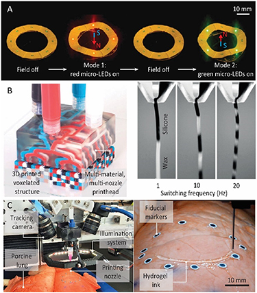
Figure 24. Examples of potential directions for future advancements in the 3D printing of soft electronics. (a) Reconfigurable electronic device with modifiable modes of functionality based on the direction of an applied magnetic field. Adapted by permission from Springer Nature Customer Service Centre GmbH: Springer Nature, Nature [120], Copyright 2018. (b) Voxelated printing via a novel printhead design that allows for the extrusion of multiple materials from each nozzle controlled by the switching frequency. Adapted by permission from Springer Nature Customer Service Centre GmbH: Springer Nature, Nature [121], Copyright 2019. (C) 3D printing of a soft, ionic hydrogel-based sensor on a 'breathing' porcine lung for in situ monitoring of deformations. Adapted by permission from [122]. © The Authors, some rights reserved; exclusive licensee AAAS. Distributed under a Creative Commons Attribution NonCommercial License 4.0 (CC BY-NC) http://creativecommons.org/licenses/by-nc/4.0/. The figures in (C) were modified by adding extra labels.
Download figure:
Standard image High-resolution imageThe poor resolution of printed features, non-uniformity of the printed layers, and print defects are some of the critical culprits impeding the performance of 3D printed electronics. These issues can be addressed by developing strategies at the material level, such as careful selection of co-solvents for optimizing the uniformity of the printed layers upon drying [115]. Alternatively, the coffee-ring effect can be exploited, rather than suppressed, to achieve feature sizes that are substantially less than the inherent resolution of the printed pattern [123]. For instance, by controlling the evaporation rate and drying process, or optimizing substrate wettability, thin line features comprising clusters of nanoparticles can form at the edges of the printed pattern [123]. This is analogous to the 'multiple patterning' strategy commonly used in the semiconductor industry to bypass the diffraction limited resolutions of conventional lithography techniques. Finally, a combination of digital image analysis and lubrication theories [124] can be applied at the process level to develop strategies for in-situ monitoring and concurrent adjustment of the printing parameters to minimize the print defects.
An additional area of focus should be to improve the scalability and mass production of 3D printed soft electronics. For instance, implementation of multi-material, multi-nozzle printheads that enable fast switching between multiple materials from each individual nozzle for voxelated printing of soft materials can facilitate increased process throughputs with reduced fabrication times (figure 24(b)) [121].
Eventually, to be compatible with the wave of industry 4.0, the 3D printing process needs to become more autonomous and adaptive. Advances in this direction could build upon recent efforts which incorporate closed-loop machine learning algorithms with real-time scanning and computer vision into the printing process, to track the motion when printing on a moving freeform object. This can also be used to capture the local deformations when printing on soft surfaces, which our group recently demonstrated via the 3D printing of a soft hydrogel strain sensor on a breathing lung (figure 24(c)) [122].
Concluding remarks
Recent advances in 3D printing suggest that this technology may have substantial promise in the development and fabrication of soft electronic devices; however, the field is still at a nascent stage. Innovations in this area have been driven by the development of materials with enhanced properties and functionalities, novel device designs, and advanced printing algorithms and methodologies. Yet, the field must overcome several challenges associated with the printable materials, device performance, and printing processes prior to widespread adoption at massive scales. If successful, the field could lead to a paradigm shift in which 3D printing platforms will become more mobile, ubiquitous, autonomous, and compact. They will be integrated with other robotic technologies and no longer perceived as means for solely dispensing materials, but rather, as integral components within larger robotic systems that can perform numerous tasks in various settings for the on-demand fabrication of functional electronics and devices. We also envision that electronic devices will be printed from one's own cell phone, such that the electronics replicate by printing electronics.
Acknowledgments
We acknowledge the National Institute of Biomedical Imaging and Bioengineering of the National Institutes of Health under Award No. DP2EB020537. The content is solely the responsibility of the authors and does not necessarily represent the official views of the National Institutes of Health. M C M is co-inventor on an issued 3D printing electronics patent: M C McAlpine, Y L Kong, '3D Printed Active Electronic Materials and Devices.' US Patent 9887356 issued 6 February 2018. G H is currently an employee of Seagate Technology.
13. Compact modelling for flexible integrated electronics
Ling Li1,2, Benjamin Iniguez1,3 and Yvan Bonnassieux1,4
1 Institute of Microelectronics, Chinese Academy of Science, People's Republic of China
2 University of Chinese Academy of Sciences, Beijing 100049, People's Republic of China
3 Universitat Rovira i Virgili, Tarragona, Spain
4 CNRS, École polytechnique, IP Paris, Palaiseau, France
Status
TFTs in various semiconductor technologies, including amorphous silicon (a-Si), polycrystalline silicon (poly-Si), amorphous oxide semiconductor (AOS) and OSC, provide abundant choices to accommodate diverse flexible integrated electronics applications. Implementation of these applications, including active matrix reflective or emissive displays, imagers, radio-frequency identification, and wearable sensor systems, need different considerations in terms of performance, cost, area and mechanical flexibility.
Unusually TFT is unipolar device and have no basic structure like CMOS inverter or amplifier, all operation of the unipolar circuits is achieved by clock signals controlling absolute transistors. Only one transistor model can be employed in unipolar circuit simulations rather than two (one for nMOS and the other for pMOS devices) in CMOS. To enable efficient design of circuits and systems, compact models are needed for those TFTs to accurately describe their electrical characteristics and be incorporated into circuit simulators to perform circuit-level simulations (figure 25). The earliest developed TFT compact models were for a-Si and LTPS TFTs by Shur et al in 1997 [125]. The models are threshold-voltage based, and define the field effect mobility as the usual crystalline silicon carrier mobility scaled by the ratio of the free carrier density to the induced total carrier density. Both current–voltage and capacitance models were developed, and for the poly-Si TFT model, both the kink effect and the short channel effect were taken into account. The models are named as RPI a-Si TFT and poly-Si TFT models, and have been widely adopted in commercial circuit simulators for practical circuit simulations.
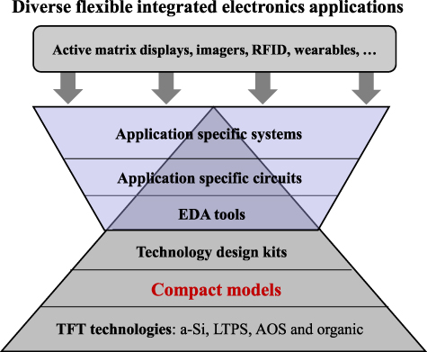
Figure 25. Illustration of the overall design flow for TFT based circuits and systems driven by the diverse applications of flexible integrated electronics. Compact models are important to link the various TFT technologies to circuit and system design.
Download figure:
Standard image High-resolution imageAfter that, lots of efforts have been devoted to new material TFTs, including OSC TFTs (OTFTs) and AOS TFTs. The models for OTFTs and AOS TFTs must consider different and specific DOSs and dominant transport mechanisms. Li et al developed OTFT compact models with variable range hopping theory and two exponential DOSs functions by neglecting free carriers [126]. Iñiguez et al showed that an accurate OTFT compact model was able to be obtained by assuming only one exponential DOS with the variable range hopping theory and assumption of no free carriers [127]. The model has a similar formulation as the RPI one and allows to apply direct methods for parameter extraction, which is called a unified modelling and extraction method [128]. Bonnassieux and Horowitz et al implemented a more physical approach for OTFT compact modelling with Gaussian distribution of DOS for amorphous OSC and a power law for mobility and contact résistance [129].
For AOS TFTs, Nathan et al derived a compact model for AOS TFTs, which included as transport mechanisms trap-controlled transport, free carrier movement and percolation [130]. Meanwhile, it was reported that, for mature AOS TFT technologies, the deep DOS is negligible, and an accurate model can be obtained assuming only the tail DOS [131]. Li et al extended the RPI model to be surface potential based, which avoided the problem of defining the threshold voltage, and showed good symmetry for circuit design [132]. Based on the surface potential model, various improvements have been made, with consideration of more physical effects and parameter extraction methods.
Consequently, compact models for both AOS TFTs and OTFTs are presently making their great steps towards practical applications and into not only academic research, but also industrial environments.
Current and future challenges
Although there has been tremendous progress over the past 20 years, the TFT compact models still need to be more physical-based, more accurate, more easily to be implemented and of less computation cost for industrial applications. For example, most of the compact models need to have the trap DOS distribution or mobility parameters in advance, but there is lack of effective extraction methods. More remarkably, the discrepancy between the model and the experiment data might vary significantly among different fabrication technologies, and the physical relationship between the model parameters and the processes is still lacking.
On the other hand, non-quasi static effects need to be incorporated into the compact model for higher frequency circuit simulation [133]. However, more physical effects need to be accounted for higher frequencies. Currently, most of the approaches at high frequencies are based on an equivalent circuit, but a fast compact model needs to take into account these effects in an analytical way in the core model structure.
Regarding the parameter extraction, significant progress has been made via fitting, some of which are based on direct extraction. New approaches such as machine leaning based techniques allow for users to obtain parameter values very quickly. Nevertheless, it remains grand challenges to develop a physical-based universal compact model with ease of parameter extraction for TFTs in various technologies and over wide temperature range.
In addition, compact models for TFTs still need to become much faster. Taking the example of active matrix backplanes for high resolution displays, the numbers of TFTs to be simulated could reach 10 million, but the current simulation speed is still very slow. There is potential of improving the simulation speed by two orders of magnitude, but not at sacrifice of accuracy.
Advances in compact modelling to meet challenges
To meet the above challenges for TFT compact models, more technology development is needed. Threshold voltage-based models could be replaced by the surface potential based model, which would allow to decrease the parameter number and improve the circuit simulation convergence. Furthermore, physical models of leakage current, subthreshold characteristics, contact resistance, short channel effects, frequency dispersion, aging, and process variations are of great potential to be improved for model accuracy and universality for different technologies (figure 26). Low frequency noise modelling is also important for flexible TFTs to be used in low power analogue design [134]. Depending on the TFT technologies, the low frequency noise could be dominated by either carrier number fluctuation or mobility fluctuation. Finally, new computation technologies, such as parallel algorithms or matrix decomposition, need to be considered for fast TFT circuit simulation speed, and compact modelling needs to consider that.
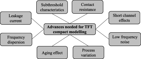
Figure 26. Summary of the required technology advances for TFT compact modelling to meet the circuit and system design with flexible integrated electronics.
Download figure:
Standard image High-resolution imageConcluding remarks
Despite the progress made with TFT compact models, there is still significant room for improvement. The key aim would be further development of the physical models with efficient parameter extraction techniques and better accuracy. In addition, more work needs to be carried out for accurate transient, frequency and noise models to support various circuit simulations. Furthermore, compact modelling needs to consider new computation algorithms for fast TFT circuit simulation.
Acknowledgments
This work was supported in part by National key research and development program (Grant No. 2018YFA0208503), by the Opening Project of Key Laboratory of Microelectronic Devices and Integrated Technology, Institute of Microelectronics, Chinese Academy of Sciences, and by the National Natural Science Foundation of China (Grant Nos. 61725404, 61890944, 61874134), by the Beijing Training Project for the Leading Talents in S&T under Grant No. Z151100000315008, by the Strategic Priority Research Program of Chinese Academy of Sciences (Grant Nos. XDB30030000, XDB12030400, XDB30030300). Besides, this work was also supported by the 645760–DOMINO–H2020-MSCA-RISE-2014('DOMINO Project'), a MSCA-RISE-2014 European Union funded project.
14. Design automation for flexible printed electronics (FPEs)
Leilai Shao1, Tsung-Ching Huang2 and Kwang-Ting Cheng3
1 ECE Department, UC-Santa Barbara, United States of America
2 Hewlett Packard Labs, Palo Alto, CA, United States of America
3 Hong Kong University of Science and Technology, Kowloon, Hong Kong
Status
Novel FPEs applications such as health-monitoring patches and artificial skins [135, 136] will need a design automation framework and EDA tools to perform system simulation and design verification. Due to low cost and low temperature printing processes for FPE, the performance variations and long-term degradation due to mechanical bending, stretching and twisting during the use remain a significant challenge to FPE designers. We first elaborate aforementioned design challenges, and then provide an overview of needed advances in design automation, PDK, and multi-physics analysis to alleviate these design challenges encountered in various FPE applications.
Current and future challenges
One driving force for advancing the FPE technology is the strong need for thinner, cheaper, and large-area electronics to meet the requirements of flexible displays, healthcare patches, and low-cost IoT. With the advances of FPE materials, printing processes, and FPE devices such as TFTs, an FPE sensor array, illustrated in figure 27, has become a reality for a wide range of applications. Among flexible substrates, plastic films such as polyimide (PI), polyethylene terephthalate (PET), or thermoplastic polyurethane are popular choices due to their low cost and bendable form factor. However, the process temperature of FPE is thus limited by the melting temperature of the plastic films that is usually lower than 200 °C. The compatible TFT technologies such as organic, metal oxide, and CNT generally suffer from inferior carrier mobility, only mono-type (p- or n-type only) device being available, and encountering large process variation, compared to conventional silicon electronics on silicon wafers. AM such as screen printing, ink-jet printing, or R2R imprinting, while contributing to lowering the manufacturing cost, limits the minimum feature sizes and the FPE circuit performance. The FPE circuit may also suffer from performance degradation due to continuous mechanical deformation such as bending or stretching. Under the aforementioned constraints and limitations, design optimization including multi-physics modelling and simulation is essential for meeting the performance target under the usage scenarios. The modelling, simulation, and design automation framework for FPE design have advanced enormously in the past few years while there still exists a significant gap between the needs and the current solutions, demanding more R&D efforts in design automation to close the gap.

Figure 27. (Left) A conceptual drawing of an FPE sensor array that is composed of an array of FPE sensors, driving circuitry, and signal amplification on a thin and flexible substrate. The thickness of the FPE sensor array is usually less than 10 µm, which enables a conformal form factor for such an array to be applied to non-planar surfaces such as human body. (Right) 3D view of a FPE circuitry that is usually composed of multiple layers of FPE devices such as transistors, resistors, capacitors, and inductors, as well as various sensors and antennas connected by the printed traces and laser or mechanical drilled through-layer vias [137]. The process temperature of FPE is usually lower than 200 °C to accommodate low cost plastic substrates such as PET. Reproduced with permission of ACM (Association for Computing Machinery) from [137].
Download figure:
Standard image High-resolution imageAdvances in design and automation to meet challenges
Among aforementioned FPE design challenges, addressing the broken link between FPE manufacturing processes and EDA tools is considered the most critical task. In silicon CMOS industry, a PDK, together with a powerful suite of EDA tools, enables circuit designers to design sophisticated circuits manufacturable by CMOS foundries in large quantities. With a similar vision, a PDK for FPE and FHE has been developed recently [138, 139]. FHE, which enhances FPE through introducing heterogeneous integration of thinned silicon chips (ex. <50 µm thick) with FPE elements on a flexible substrate, makes desirable features, such as near-sensor computing and wireless communication, feasible. The FPE/FHE ecosystem enabled by the PDK is illustrated in figure 28. The FPE/FHE designers can conduct various design simulations under target operating temperatures and bending radii and in turn produce manufacturable design database with the aid of EDA tools and PDK [137, 139]. The PDK could also include FPE/FHE process-validated design IP blocks such as Pseudo-CMOS design IP for digital, analog, and power circuits [140] which relieve the designers from tedious and repetitive tasks of handling device-level details. In addition to the FPE/FHE PDK, customized place-and-route (P&R) algorithms for physical design flow is also required in order to accommodate the bending use cases for TFT circuits. The study in [141] relied on a statistical timing analyzer (STA) to identify bending hotspots, and used the derived information together with TFT bending models [142] to generate a hotspot mapping for guiding circuit layout, followed by the cell placer's simulated annealing process for finding the optimized cell placement to minimize timing degradation under bending. The study in [143] further suggested inclusion of both mechanical strain and temperature drift's impacts on TFT circuit's performance in layout optimization. For bending or other use cases that require mechanical deformation or thermal cycles, FPE/FHE multi-physics models for electrical, mechanical, and thermal interactions must be comprehensive and accurate in order to derive useful information from multi-physics simulation. A recent study [144] investigated multi-physics 3D finite-element models (FEM) considering both mechanical and electrical aspects of Aerosol jet printed (AJP) and screen printed (SP) transmission lines and power inductors. The results showed strong correlation between FEM and measurement data of AJP transmission lines under flat cases and suggested insignificant changes for insertion loss S21 and return loss S11 under bending. However, there still exist larger discrepancy between FEM and measurement data as well as significant changes for S21 and S11 under bending for SP transmission lines and power inductors, which suggested that FPE multi-physics modelling and simulation methodology are still in the infancy and in need of further research.
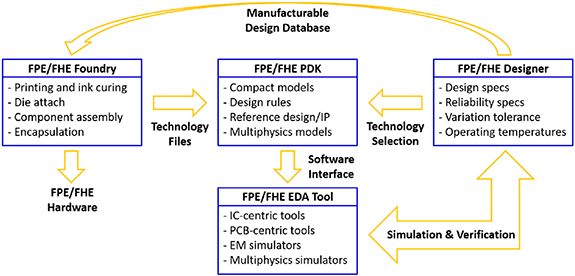
Figure 28. The FPE/FHE design-manufacture ecosystem enabled by the PDK. The PDK includes the latest technology files that represent the manufacturing capability and target performance in the forms of design rules and compact models. The PDK could also include multi-physics models for multi-physics simulation under various thermal or bending conditions, as well as design intellectual property (IP) blocks or reference designs for FPE/FHE designers. The PDK also needs software interfaces for IC-centric or PCB-centric EDA tools in order to perform simulation and physical design verification against the design rules. The designers can also use electromagnetics (EM) or multi-physics simulators with the PDK for radio-frequency (RF) or bending use cases.
Download figure:
Standard image High-resolution image
Concluding remarks
Large device variations, device defects and multi-physics considerations of FPE/FHE must be tackled before FPE/FHE can be broadly deployed in next-generation wearable and IoT hardware. While continuing reduction in device variation/defects can be expected, novel solutions at the circuit-, architecture-, and system-levels are indispensable in order to achieve sufficiently high reliability and cost-effectiveness for consumer and enterprise applications. Furthermore, FPE/FHE designs will also require the support of a production-ready PDK, a suite of design automation tools, including a comprehensive simulation framework for multi-physics analysis.
Acknowledgments
This material is based, in part, on research sponsored by Air Force Research Laboratory under agreement number FA8650-15-2-5401, as conducted through the flexible hybrid electronics manufacturing innovation institute, NextFlex. The study was also partially supported by a General Research Fund (GRF) grant from Research Grants Council (RGC), Hong Kong (HKUST 16203319).
Data availability statement
No new data were created or analysed in this study.