

Abstract
Transparency and bendability are some of the most attractive unique selling points for organic light-emitting diode (OLED) lighting, enabling a variety of new application possibilities for industrial and private end-users. The roll-to-roll (R2R) OLED fabrication based on thermal evaporation offers a fast, continuous-running solution for producing flexible OLEDs at a lower cost. In this work, R2R fabricated large-area highly transparent thermal co-evaporated Ca:Ag (2:1 vol.%) top-electrode with mean transmittance of 64% over the visible range and a corresponding sheet resistance of as low as 21 Ω sq−1 was achieved. By increasing the film thickness to 24 nm, the sheet resistance can be further reduced to 12 Ω sq−1, albeit with a lower mean transmittance of 58%. The Ca:Ag electrode demonstrates a high mechanical durability through 1000 bending cycles, which is highly desirable as a characteristic for flexible electronics, as well as for the R2R fabrication. Finally, the stability of the Ca:Ag electrode in vacuum and ambient was studied as well.
Export citation and abstract BibTeX RIS

Original content from this work may be used under the terms of the Creative Commons Attribution 4.0 license. Any further distribution of this work must maintain attribution to the author(s) and the title of the work, journal citation and DOI.
1. Introduction
Organic light-emitting diode (OLED) technology has found application in a broad range of scenarios in our daily lives, due to its high efficacy, rich color selections, flexible design forms, area lighting, and simple housing without specific heat-dissipation requirements, as compared to inorganic LED technology. In recent years, application of OLEDs with high transparency has become a trendy research topic with the potential to enable many more application possibilities in both OLED display [1, 2] and OLED lighting [3–5] applications. OLED technology has been showing great potential to be an extension for current lighting solutions. However, the obstacle between current OLED products and commercial end-users is the still mainly caused by the high cost of OLEDs. Therefore, research efforts are dedicated towards OLED fabrication in a novel roll-to-roll (R2R) process based on thermal evaporation of organic small-molecule materials as has been already demonstrated and commercialized for organic photovoltaic production [6]. The feature of R2R fabrication provides the possibility of producing OLEDs in an almost endless way, given sufficient material supply. The novelty and the advantage of R2R pilot line is that it produces OLEDs in rolls instead of sheets as is done in conventional production lines, saving both production time and production-related costs. It offers a solution to reduce the price of OLEDs and paves the way to make OLED products more affordable to consumers. Combining R2R fabrication of flexible OLEDs with high device transparency is of particular interest for the quickly growing OLED market.
Ag transparent thin film with Al seed layer has been previously demonstrated to successfully serve as a transparent top-electrode for R2R OLEDs [7]. However, due to the demand of flexibility during the R2R process as well as high transparency along with low electrical sheet resistance for the top electrode, Ag or Al/Ag electrode with Al as seed layer [8] are not sufficient for fabricating OLEDs with high transparency. Therefore, a new material system compatible with thermal evaporation is required. Co-evaporated metal films [9–13] have been recently reported to serve as electrodes for organic optoelectronic applications with higher transmittance as compared to single Ag thin film. We chose to investigate the co-evaporated Ca:Ag system due to its high transmittance across the entire in the visible range, which is desired characteristic for both monochromatic and white OLEDs.
In this work, a R2R fabrication of a high performance transparent Ca:Ag top electrode for flexible large area OLED lighting application will be presented. We demonstrate an improved average optical transmittance of 64% and a low sheet resistance of 21 Ω sq−1 at Ca:Ag layer thickness of 18 nm. The co-evaporated electrode does not lead to a light out-coupling enhancement on PET substrate as compared to a standard transparent Al/Ag top-electrode. The properties of the R2R prepared top electrodes are comparable to those fabricated by standard evaporation on small-area lab-scale devices [14], considering the increased thickness used in this work as is required for reliable and robust R2R-fabricated top-electrodes.
2. Experimental
2.1. Sample preparation
R2R vacuum deposition of small molecule OLEDs on flexible substrates is carried out in the RC300-MB R2R vacuum coater (supplier Von Ardenne GmbH [15]). The machine enables processing of metal, plastic substrates or ultra-thin glass with a maximum width of 300 mm and a thickness of 70–500 µm. With integrated 14 organic linear sources, multi-unit OLED stacks (e.g. for white OLED) can be realized [16–18]. The flexible substrate on the roll will be first loaded on the two winders as shown in figure 1, which are used for unwinding (right side blue winder) and rewinding (left side blue winder) of the substrate during deposition, and the substrate is led through the 14 organic linear sources by the deposition drum with a diameter of 2 m. After the organic layer deposition, the substrate will come to the metal evaporators for top electrode deposition. Lastly, the completely coated OLED stack will then be encapsulated in an inert atmosphere, which was described in previous work [16]. The last step will be the separation of the OLED modules by either mechanical cutting or laser separation, depending on the substrate and encapsulation materials.

Figure 1. A schematic of the roll-to-roll OLED fabrication machine, using flexible substrates with typical width of 300 mm. The detailed top-view layout of the metal sources is enlarged.
Download figure:
Standard image High-resolution imageThe configuration of the metal source hardware (CreaVac GmbH) was two point-sources (Al/Ag) seated in two adjacent separated compartments, which enabled the deposition of Al and/or Ag thin films as the electrode materials. In order to implement the idea, the metal chamber has to be reconfigured, adding one extra metal source next to the Ag source (figure 1), which enables the co-evaporation of Ag with one other metal material. The Al and Ag raw materials are metal wires in spool, with high purity of Al 99.98% and Ag 99.95%, loaded on a wire-feeding system controlled by the software program with adjustable feeding speed (typical speed 30–80 mm min−1, depending on the deposition rate) of the wires into the crucible or the evaporation boat. As the point-source evaporators are used for a moving substrate with a typical width of 300 mm, the thin film cross-homogeneity of metal coatings are regulated by the metal aperture placed on top of the metal source compartment with an optimized shape of the opening to achieve a homogeneous coating thickness over the substrate. The thickness homogeneity of each material is individually controlled during the calibration, or the so-called tooling process [19] with one or several film thickness variations (more information see SI 1 (available online at stacks.iop.org/FPE/6/035001/mmedia)). The mixing ratio (MR) is volume ratio in this work, therefore the deposition rate is controlled to realize the MR with defined film thickness (e.g. 18 nm Ca:Ag 2:1 means 12 nm Ca + 6 nm Ag in co-evaporation).
In this work, 300 mm wide flexible PET substrate in rolls (Melinex ST504 125 µm, DuPont Teijin Films) were used for the transmittance and reflectance, sheet resistance, atomic force microscopy (AFM), x-ray photoelectron spectroscopy (XPS), x-ray diffraction (XRD) and mechanical characterization, and the ultrathin glass substrate with PET carrier foil (50 µm NEG G-Leaf ™ Glass + 75 µm PET) in rolls with a width of 300 mm was used in the encapsulation experiment for optical characterization, as isolation of the reactive Ca:Ag electrode from moisture and oxygen in the ambient is required. In the encapsulation experiment, ultrathin glass (thickness 50 µm) on PET carrier foil was used as the substrate. For the encapsulation, it was only the ultrathin glass (50 µm) with already laminated pressure sensitive adhesive (PSA), which is a commercially available material (Tesa 61500) including getter material, and the encapsulation process was done at the same R2R OLED machine in vacuum right after the deposition by laminating the encapsulation glass from the left interleaf winder in figure 1 onto the samples on the re-winder. The substrates used in this work were all bare substrates without anode material. The base vacuum of the deposition is in the range of 10−6 mbar. Since the PET is stored under ambient condition and contains considerable amount of water [20], an out-heating pre-treatment in R2R process (winding speed is 200 mm min−1) with a heating temperature of 60 °C on the deposition drum will be performed twice to outgas the moisture before thin film deposition. The out-heating pre-treatment of the substrate was done by unwinding and rewinding the substrate from the unwinder and to the rewinder respectively, between which the substrate was laid on the deposition drum that rotates at the same substrate speed and its surface temperature is configurable for the heating purpose (please refer to the schematic in figure 1), afterwards a second out-heating treatment will be performed by wingding the substrate backwards from the rewinder to the unwinder. The ultrathin glass substrate with PET carrier foil was out-heated twice in R2R with 30 °C and kept in vacuum over two days for further dry-out. During the out-heating process, a clear out-gassing of residual water in the substrate can be observed, causing the vacuum pressure to increase up to the level of 10−5 mbar. After this step, the already out-heated substrate will then be ready for the thin film deposition without vacuum break. The deposition of the thin films, in this case metal thin films, will then be performed with the substrate winding speed of 200 mm min−1. The web tension applied for winding the PET substrate during the deposition was 100 N, and for the glass substrate it was 150 N. For encapsulation, the web tension applied on the encapsulation glass was 50 N.
2.2. Characterization
Optical spectra of transmittance and reflectance were measured by the AudioDev inline spectrometer system (NXT GmbH) in vacuum in-situ and by Lambda 900 UV–VIS–NIR Spectrometer (Perkin-Elmer) in ambient ex-situ. The wavelength range between 320 and 800 nm was selected for the analysis. Substrate correction is not applied for the optical measurement results.
Sheet resistance was characterized by the Veeco FPP-5000 4-Point-Prober, and five measuring spots across the 300 mm substrate width were taken at a distance of 50 mm, 100 mm, 150 mm, 200 mm and 250 mm to the edge of the same side. Each spot was measured three times for the average sheet resistance calculation. The error bar in figure 2 represents the standard deviation of the sheet resistance of the five measuring spots across the width, representing the homogeneity of the film over its width.

Figure 2. Optical transmittance spectra of Ca:Ag coatings on PET substrate measured (a) in vacuum and (b) after one day storage in the ambient condition.
Download figure:
Standard image High-resolution imageSurface morphology and roughness of the thin films were measured with AFM by the Nanite B system (NANOSURF AG), based on a measuring area of 5 × 5 µm2 with metal coatings on the PET substrate, as well as with the SEM by field emission SEM (SU 8000, Hitachi).
Chemical composition was analyzed using XPS with a PHOIBOS 100 analyzer system (Specs) at a base pressure of 10−10 mbar using a monochromated Al Kα source (1486.6 eV) and a pass energy of 20 eV.
Phase composition of the materials were investigated by the XRD with the XRD 3000PTS (GE Inspection Technologies). Cu K-alpha x-ray was used for the measurement with a grazing incident angle of 1. The sample was stored and measured in the N2 environment after the deposition to avoid degradation as much as possible.
Mechanical bending tests of the thin metal coatings were performed by the Yuasa Endurance Testing Jig—Demo 70 (Yuasa System Co., LTD), with the samples size of 15 × 5 cm2. The bending radius was fixed at 5 mm and the bending speed was set at 30 r min−1. The bending angle was varied from 0 up to 90° in order to test the durance of these thin Ca:Ag coatings under varying stress. Resistance with different bending angles was measured by a multi-meter connected to the two narrow ends of the long samples, which was fixed using aluminum conductive tape onto the metal coating. For the test with varying bending cycles up to 1000 times, sheet resistance was measured with a 4-Point-Prober at the middle of the long stripe sample where the coatings were most stressed during the bending cycle test. The bending angle used for this test was set at 60°.
3. Results and discussion
3.1. Transparent Ca:Ag electrodes
Ca:Ag coatings with MR of 2:1 and 4:1 in vol% are selected for optimization with three different film thicknesses (18, 21, 24 nm), in order to achieve an optical transmittance of more than 50%, and a goal sheet resistance lower than 20Ω sq−1. The sheet resistance and transmittance of 19 nm Ag film is added in figure 3 in blue dashed line as a reference (for Ag thin films at other thicknesses, please refer to SI 2). Single Ca film was practically not possible to measure in the air. All the MRs used in this work are in volume percentage.
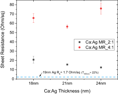
Figure 3. Sheet resistances of Ca:Ag coating with two different mixing ratios (2:1, 4:1) at three different thicknesses (18, 21, 24 nm). The blue dashed line shows the sheet resistance 19 nm Ag coating as a reference.
Download figure:
Standard image High-resolution image3.1.1. Electrical sheet resistance
The sheet resistance was measured immediately after the thin film deposition. The Ca:Ag coatings with 2:1 MR have shown a sheet resistance of 21 Ω sq−1 at a thickness of 18 nm, with a decreased sheet resistance of 12 Ω sq−1 at a higher thickness of 24 nm (figure 3). While the sheet resistance of 2:1 MR films is, as expected, reduced in a quasi-linear fashion with increasing thickness, samples with a 4:1 MR do not follow the same trend. In particular, the 24 nm thick samples exhibit a higher than anticipated sheet resistance of 70–80 Ω sq−1, which we attribute to non-ideal deposition conditions. Regardless, for all thicknesses, electrodes with MR 4:1 have higher sheet resistances as compared to those with a MR of 2:1.
3.1.2. AFM surface roughness
Despite the different MRs and film thicknesses of the Ca:Ag coatings, no noticeable changes to the surface roughness of the layers was observed when characterizing their surface microstructure by AFM. The AFM results (see table 1) showed rather consistent root-mean-square (RMS) surface roughness that varied between 1.4 and 3.0 nm over the characterized area of 5 × 5 µm2 for all the samples. In many of the samples, a peak-to-valley roughness larger than the film thickness is observed, suggesting a high dependence of the P-V roughness on the local surface quality of the substrate, which is possibly caused by the defects or particles on the substrate surface (comparing AFM images in SI 3 and SI 4).
Table 1. Surface roughness measured by AFM of the Ca:Ag thin films with varying mixing ratios and varying film thickness on PET substrate.
| Ca:Ag ratio (in vol.) | Film thickness (nm) | Surface roughness by AFM | |
|---|---|---|---|
| RMS (nm) | P-V (nm) | ||
| 2:1 | 18 | 1.6 | 30.2 |
| 21 | 2.2 | 54.3 | |
| 24 | 1.9 | 26.2 | |
| 4:1 | 18 | 3.0 | 28.0 |
| 21 | 2.8 | 42.0 | |
| 24 | 1.4 | 14.2 | |
The Ca:Ag coatings have shown smooth surfaces from the RMS roughness in table 1, which is comparable to the roughness of anode ITO coatings reported in the literature [21, 22]. The high PV roughness can be attributed to the PET substrate, but the issue present in this experiment will not be problematic for OLED fabrication, since extra planarization layer will be utilized prior to the OLED deposition to cover the possible imperfections [23].
3.1.3. Optical spectra in vacuum and air
The optical spectra of all layers were measured both inline in vacuum and also under ambient condition after the samples were taken out from the coating machine. The transmittance spectra measured in the vacuum have a typical curve shape as closed thin transparent Ag thin films [8, 12, 24], whose spectral transmittance decreases with the increasing wavelength in the visible range. However, the spectra evolve into an almost flat curve over the whole visible spectrum after exposure to the ambient for approximately 24 h (see figure 2(b)). Following this, the 18 nm Ca:Ag layer with MR 2:1, for example, shows a maximum transmittance of 70.3% at around 380 nm, and an average transmittance of 64% over the 320–800 nm range, without any out-coupling enhancement layer.
The increase of the transmittance reaches 30% for 18 nm Ca:Ag coating with MR 2:1, and is as high as 36% for the 21 nm thick Ca:Ag film of MR of 4:1 at 800 nm. This phenomenon has not been explicitly reported before, as it can very easily go unnoticed if the evaporated Ca:Ag samples are not characterized directly after fabrication under vacuum condition prior to their measurement in the ambient. It is also noteworthy that the significantly modified transmittance induced by the atmosphere of all films at the same MRs tends to be very similar (MR 4:1) or very close to each other (MR 2:1) despite the different film thicknesses, which is unexpected for metallic coatings.
These results suggest that the Ca:Ag mixed electrodes undergo a reaction with the atmosphere gases, such as H2O, O2 and CO2, which starkly modifies their optical properties. This change has likely gone unnoticed in previous reports [9, 14]. We stress that such an evolution in the optical properties upon exposure to the ambient can influence the performance of Ca:Ag thin films as electrodes for applications in organic opto-electronic devices and thus should be characterized in detail.
3.1.4. Transmittance and sheet resistance stability
In order to evaluate the changes in the optical and electrical properties of the Ca:Ag mixed layers over time, we monitored both their transmission and sheet resistance over a period of 30 days (figure 4). We note that the electrical sheet resistance measurement cannot be performed in the R2R equipment under vacuum condition, but the optical spectra were measured using the inline optical spectrometer.

Figure 4. The development of transmittance (at 550 nm) and sheet resistance in the air of the Ca:Ag coatings with MR 2:1 and 4:1 were plotted in the graphs above after 0, 1, 7, 30 days. In addition, transmittance measured in the vacuum during the deposition process using inline spectrometer is also included.
Download figure:
Standard image High-resolution imageSimilar to what has been described above, the optical transmittance (at 550 nm) of the Ca:Ag mixed films significantly increases after just one day of storage in the ambient. For example, the transmittance of the 18 nm thick 4:1 MR film has increased by approximately 21%, while the 2:1 MR film of the same thickness has increased ∼27% within 24 h. After this initial change, the transmittance of all films remains largely unchanged. This observation supports the idea that exposure to the ambient leads to a quick reaction between the electrodes and the atmospheric gases. Since the measurement at day 0 was performed in the ambient directly after the deposition of the mixed metal electrodes, it can be estimated that the reaction time is that of minutes to hours.
As mentioned above, we were only able to measure the sheet resistance upon removing the films from the R2R machine. We observe minimal changes in the sheet resistance of Ca:Ag films with a MR of 2:1 over the period of 30 days. The 4:1 MR films, however, show an increase in sheet resistance. For example, the sheet resistance of the 18 nm thick film has increased from 66 Ω sq−1 to 76 Ω sq−1, with 50% of this increase occurring within the first 24 h. We thus conclude that films with a 2:1 MR exhibit not only an overall lower sheet resistance (<21 Ω sq−1), but are also considerably more stable over time, when compared to those fabricated with a MR of 4:1.
3.2. Structural and composition investigation
To monitor the composition of the mixed electrodes, XPS measurements were performed on a freshly fabricated 21 nm Ca:Ag (2:1) film (denoted as 'fresh' in figure 5) and after storing the very same film in ambient conditions for nine days ('degraded' in figure 5). The fresh sample has been exposed to the ambient for a short time (ca. 30 min) due to the transfer from the R2R coater to the N2 environment prior to XPS measurement.
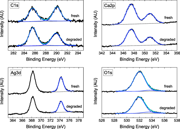
Figure 5. XPS spectra showing the C 1s, Ca 2p, Ag 3d and O 1s peaks of a Ca:Ag film. The measurements were performed on a freshly fabricated film (fresh) and after storing the very same film in ambient conditions for nine days (degraded).
Download figure:
Standard image High-resolution imageThe XPS measurements show that the fresh film exhibits Ca 2p and Ag 3d doublet peaks with peak binding energies matching CaO [25, 26] and metallic Ag [27], respectively. The O 1s spectrum consists predominantly from a singlet at 531.9 eV, which is associated with the formation of metal oxides (i.e. CaO) at the surface of the film. A small contribution at a binding energy of 533.6 eV is also observed and is associated with O–H groups. The presence of such hydroxyl groups is common to natively formed oxides of various metals [28, 29].
After storing the Ca:Ag film in ambient conditions for nine days, the peak binding energies remain unchanged, as shown in figure 5, indicating that no new chemical bonds have formed. The signal associated with O–H groups (533.6 eV) slightly increased from 2.3 at.% to 4.0 at.%, possibly due to formation of additional hydroxyl groups at the surface of the films. The XPS results demonstrate that the formation of surface oxides is a fast process that occurs within minutes of removing the films from the vacuum system. Moreover, once the mixed metal electrodes have reacted with oxygen, no significant compositional changes occur upon long-term exposure to the ambient. These results are in good agreement with the previous optical and electrical characterization results, which confirm the stability of the electrodes.
The XRD measurement of the 21 nm thick Ca:Ag (2:1) film deposited on a glass substrate shows clear diffraction peaks from Ag, however no peaks from Ca or its possible derivatives (e.g. CaO, Ca(OH)2) [30, 31] can be observed in the XRD pattern (figure 6(a)), suggesting that Ca or its derivative compounds in the mixed film are amorphous. The amorphous metal is likely a result of physical vapor co-deposition [32, 33], or its oxidation after fabrication. After the sample was stored in the ambient for up to 64 h (green curve in figure 6(a)), no changes in the crystalline structure were observed. The SEM image in figure 6(b) shows the topography of the film, which reveals a metal thin film with rich nanostructure, in contrast to the smooth surfaces of other metal films of the same thickness [8, 12]. The SEM image with backscattered electrons displays material contrast (figure 6(c)), allowing to distinguish between the different constituents of the film. In this image, silver appears brighter and calcium appears darker, while pores in the film structure appear black, as is indicated by arrows in the image. In the Ca:Ag mixed film, silver forms a nano-porous network with the densely incorporated calcium-rich domains, with a typical size up to ca. 20 nm, possibly protruding through the entire film thickness.

Figure 6. The (a) XRD measurement of Ca:Ag coating on glass substrate as deposited (blue), after 2 h (red) and after 64 h (green) storage in the ambient, (b) the topography-contrast SEM image of the coating, and (c) the material-contrast SEM image with the notation marked in the enlarged characteristic area.
Download figure:
Standard image High-resolution imageTaken together, these results indicate that the crystalline Ag network in the mixed film contributes to the low sheet resistance of the electrode, while the high transmittance of the mixed Ca:Ag film under ambient condition is speculated to be a combined effect of the calcium oxide domains with low optical absorption and reflection [34], acting as 'optical holes' in the film, and the extraordinary optical transmittance (EOT) phenomenon resulted from surface plasmons and the diffraction effect [35–37] of the disordered groups of 'holes' in the metal film.
3.3. Mechanical durability of the electrode
In addition to the optical and electrical requirements, the transparent Ca:Ag electrode must also be mechanically robust enough in order to be used in a R2R manufacturing process, as well as post-fabrication for application in flexible OLEDs. Therefore, mechanical bending tests with a fixed bending radius of 5 mm and varying bending angles (see figure 7(a)) were performed on 18 nm thick films of 2:1 and 4:1 MRs. The evolution of sheet resistance over 1000 bending cycles was also evaluated (figure 7(b)). The 21 and 24 nm films are assumed to behave in general similarly with the same MR, given only few nanometer change in the film thickness [38–40]. For both tests, two different directions of bending were applied in order to test pressing (folding the coating) and stretching (opening the coating) limit of the thin films as is sketched in the inset of figure 7(a).

Figure 7. Mechanical tests of the Ca:Ag coatings on PET substrate, with 18 nm thickness and two different mixing ratios 2:1 and 4:1. The size of the samples used for these tests is 15 × 5 cm2 and the bending radius is 5 mm. The electrical resistance or sheet resistance is used to monitor the mechanical influence on the coatings with respect to the bending angles or bending times at the angle of 60°.
Download figure:
Standard image High-resolution imageFor the bending angle test, all samples were bent from 0° up to 90° (figure 7(a)), and the resistance was measured at each specific bending angle simultaneously. Only the 4:1 film had shown an increase about 40% (from 263 Ω to 366 Ω) of the resistance at 90° when stretched (opening), implying possible cracks forming inside the thin film that cause this increase in the resistance of the sample. Folding the thin films, on the other hand, led to little change in their resistance. The different initial resistance of MR 4:1 sample for folding and opening tests is caused by the contacting condition, which has been minimized as much as possible by adjustment. The MR 2:1 film shows no noticeable changes in properties upon neither the opening nor the folding tests up to 90°, which demonstrates the excellent robustness of these films to the mechanical stress induced by the bending tests.
Another important factor for flexible electronics is the durability of the mixed metal electrodes, which was investigated by monitoring the sheet resistance at the stressed bent area after certain number of bending cycles with a fixed bending angle of 60°. In this test, Ca:Ag coating with 2:1 MR showed rather consistent sheet resistance even after 1000 bending cycles, with a maximum change of 2.8 Ω sq−1, for both 1000 opening and folding tests, which is consistent with previous stress test regarding bending angles. However, far higher initial sheet resistance as well as large sheet resistance variations were observed for films fabricated using the 4:1 MR, suggesting they are less suitable for application in flexible electronic devices.
3.4. Effect of encapsulation on Ca:Ag electrodes
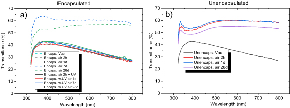
To investigate the behavior of Ca:Ag electrodes upon encapsulation typically used for OLEDs fabrication in R2R process, a Ca:Ag mixed film with a nominal thickness of 21 nm was deposited on the ultra-thin glass substrate, which was then encapsulated by another ultra-thin glass with PSA instantly after deposition in the vacuum. Several meters of the mixed metal film were left unencapsulated for comparison. The PSA on the encapsulation foil was integrated with a getter function [41] for absorbing moisture that requires UV activation, therefore the encapsulated samples were divided into UV-activated and non-UV-activated sets.
The transmittance spectra of the films under different conditions were used for the observation of the process influence. As can be seen figure 8, the transmission of encapsulated and unencapsulated Ca:Ag films were measured under vacuum and under ambient conditions after varying periods of time since having been taken out from the R2R coating machine.
Figure 8. The transmittance of 21 nm Ca:Ag coating with MR 2:1 deposited on ultrathin glass substrate (a) with and (b) without glass encapsulation measured in the vacuum as well as measured under the ambient condition (UV treatment for getter activation in adhesive).
Download figure:
Standard image High-resolution image
Figure 8(a) demonstrates that the encapsulated Ca:Ag films that had undergone a UV treatment show very similar optical properties even after prolonged exposure to the ambient (28 days) to their initial properties directly after deposition in vacuum. However, encapsulation alone, without a UV treatment, prevents changes in the optical properties only temporarily—while samples exposed to the ambient remain stable over one day, longer exposure times lead to increase in transmittance, comparable to that observed in unencapsulated films (figure 8(b)). This result clearly demonstrates the functionality of the encapsulation and the additional getter material. Only the combination of both the ultrathin glass encapsulation with UV-activated getter is effective in preventing the oxidation of Ca:Ag electrodes, while glass encapsulation alone is not able to prevent the formation of oxides over time, possibly due to the residual water incorporated inside the encapsulation [42].
4. Conclusion
This work has presented for the first time a R2R fabricated transparent Ca:Ag thin film suitable for application in large-area transparent OLEDs. The Ca:Ag electrodes with MR of 2:1 have shown low RMS surface roughness <3 nm and low sheet resistance of 21 Ω sq−1. High average transmittance of 64% in the range of 320–800 nm, (max. 70.4% at 380 nm) was achieved with the 18 nm film measured under ambient conditions, without any out-coupling enhancement. These Ca:Ag electrodes also show high mechanical stress tolerance and bending durability, which is very appealing for R2R fabrication, as well as for OLEDs or organic photovoltaic (OPV)s applications aiming at high flexibility. Compositional studies revealed that upon exposure to the ambient the mixed metal electrodes form CaO at their surface, thus leading to a change in their optical properties. When encapsulated with UV-activated getter materials, the coatings exhibit excellent stability over time. Last but not least, the results presented in this work should be important also for other mixed metal thin film electrodes, such as Mg:Ag, Al:Ag and others, which has likely gone unnoticed in previous reports on their application in OLEDs or OPVs.
Acknowledgments
This work has been partially funded by the German Bundesministerium für Bildung und Forschung (BMBF) within the project LAOLA (Large-area OLED lighting applications on thin flexible substrates, funding reference: 03INT509AF). Besides, we would also like to express our gratitude to our colleagues Julia Berger, Stefan Donath, Philipp Krampe, Thomas Modes and Michiel Top for their cordial support in the experiments and the characterization of the probes. Last but not least, we would also like to acknowledge the collaboration with Yuasa System Co., LTD (www.yuasa-system.jp/en) for providing the bending test stage that makes the mechanical tests possible for this work.
Data availability statement
All data that support the findings of this study are included within the article (and any supplementary files).