


Abstract
Neural interfaces that directly measure brain activity are increasingly employed to elucidate large-scale brain networks and treat intractable neurological disorders. Considering the softness of brain tissue, current efforts to study chronic disorders aim to minimize invasiveness. We discuss recent progress on flexible neural interfaces with high durability under bending and stretching achieved by using organic materials. Multichannel microelectrodes are usually fabricated on thin polymer substrates as sheets and needles to reach superficial and deep brain structures, respectively. An interesting recent trend is the integration of high-density microelectrodes to measure detailed brain functions. The use of numerous measurement points (the current highest values achieved are 62 500 electrodes cm–2 and 3072 channels) can increase the accuracy of brain state estimation. However, further improvement should be devised for integration in plane considering the density of 250 000 neurons cm–2 in approximate intervals of 20 μm. Meanwhile, the ultimate goal of improving flexibility in neural interfaces is long-term implantation. Widely used approaches for thinning polymers (∼1 μm) and reducing the rigidity of neural interfaces compromise robustness due to high gas permeability and water uptake. We quantitatively analyze the technical proficiency of flexible neural interfaces in vivo regarding microelectrode integration and robustness. The solution contact impedance, which is a crucial factor in microelectrode miniaturization, is exhaustively surveyed and compared across PEDOT:PSS, Au, Pt, Pt black, IrOx, gels, and other components that should be designed within the permissible source impedance for the measurement device to ensure high-accuracy and low-noise measurements of brain activity in the order of microvolts. Furthermore, we detail a multifunctional neural interface with stretchability, optical transparency, easy intraoperative handling, and flexible transistor implementation for building an active electrode array, providing a new approach for flexible interfaces in neuroscience and neuroengineering.
Export citation and abstract BibTeX RIS

Original content from this work may be used under the terms of the Creative Commons Attribution 4.0 license. Any further distribution of this work must maintain attribution to the author(s) and the title of the work, journal citation and DOI.
1. Introduction
The brain is a vast network comprising 0.1 trillion neurons that generate higher brain functions with low energy consumption of only 10–20 W [1–5]. The complexity and efficiency of the brain make it substantially different from artificial systems as a central processing unit. Thus, the elucidation of brain function has fascinated us with its deep mysteries, while brain function research is being pursued to understand and treat serious diseases. As many as 8 million people per year die from brain diseases such as stroke and dementia, and approximately 25 million people with physical disabilities need prosthetics or orthoses, while half a million people per year suffer from spinal cord injuries according to estimations of the World Health Organization. To detect, prevent, treat, and elucidate these problems, brain function research is becoming an increasingly active field [3, 6–13]. The cerebral cortex has different subregions that emphasize motor, sensory, linguistic, and other functions. For instance, the sensorimotor cortex presents distinct regions that correspond to specific body parts (e.g. hands, feet, face) and are orderly aligned, thus forming a body map [14]. The functions of each subregion are being studied to complete the brain map. More recently, neural interfaces with numerous measurement electrodes have been under development, to further investigate complex coordinated brain activity and efficiently characterize known brain functions.
The most commonly used type of multichannel neural interface uses implantable electrodes, such as Utah arrays and Michigan probes [3, 15–17]. Although such penetrating electrodes require craniotomy during neurosurgery for implantation, they allow the measurement of individual neuron activity, which is the basis of overall brain activity. Thus, an extremely rich variety of information can be extracted from implanted electrodes. Historically, hard and thick metals, as well as silicon, have been used to create implantable electrodes. However, such hard materials may cause damage to the soft brain tissue, especially for long-term use [3, 18–20]. Recently, multichannel neural interfaces that are more suitable for the soft brain tissue have been developed [21–47].
In this paper, we review flexible neural interfaces for brain implantation and summarize development trends regarding electrode density, number of electrodes, electrode impedance, total thickness, and durability. We also present an example of brain activity measurement using flexible neural interfaces and briefly analyze the performance of devices for signal processing.
2. Flexible neural interfaces
2.1. Transition from rigid to thin and soft structure
A neural interface should be mechanically flexible to prevent inflammation and damage to the brain tissue. As the brain exhibits a Young's modulus comparable to that of tofu (below 5 kPa), the stiffness of the neural interface must be reduced [19, 20]. The stiffness is proportional to both the Young's modulus and the cube of the substrate thickness. As shown in figure 1, the Utah arrays and Michigan probes were developed in the 1990s, as needle probes for implantation from the cerebral cortex into deep brain regions. These devices were applied with thin silicon (Si) technology that could bend [3, 17, 46–48]. Although these probes are robust for long-term implantation [15, 17], inflammation in brain tissue may occur given their Young's modulus, corresponding to approximately 100 GPa [48, 49]. In the 2000s, flexible neural interfaces were developed using flexible conductors, mostly thin Au, and thin polymer substrates such as polyimide (PI) [22, 50, 51], Parylene (poly-para-xylylene, PPX) [38, 52], and SU-8 with a Young's modulus of 2–5 GPa [48, 53–58]. Besides needle probes, sheet-type probes for electrocorticography (ECoG) implanted on the brain surface have been actively developed using polymers. ECoG can be directly acquired from a microelectrode array in a sheet-type neural interface that is placed on the cortex, as a non-penetrating method. The corresponding flexible neural interfaces were developed for both sheet-type and needle probes at that time.
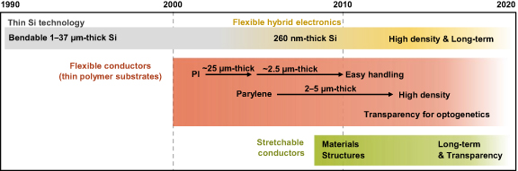
Figure 1. Chronological development of representative technology for flexible neural interfaces.
Download figure:
Standard image High-resolution imageThin-film polymers with thicknesses below 10 μm are extremely difficult to handle, given their lack of rigidity. The research group led by Rogers used silk to design materials that are rigid in air and soft after implantation [22]. They also used an implementation technique of 260 nm thick thin silicon on 12.5 μm thick PI substrates called flexible hybrid electronics [26], which is being adopted in sophisticated neural interfaces. In 2010, neural interfaces began incorporating stretchable conductors fabricated with spring-like structures or with gels and elastomers whose Young's modulus is in the order of 10 kPa–100 MPa [28, 32, 37, 44, 56, 59]. The polymeric materials in these flexible neural interfaces render them bendable and stretchable. Reports on their use have shown a steady increase through to 2020. Minimal inflammation and damage to the brain tissue are now becoming a reality for neural interfaces.
Although we focus on measurements using flexible neural interfaces, control of neural activity is also important for functional understanding and disease treatment. For instance, optogenetics has recently enabled brain activity control by fusing light stimulation and genetics (figure 1). Optogenetics controls neural activity (excitation and inhibition) by expressing light-sensitive genes in specific neurons and exposing them to light [8, 60]. Compared with conventional electrical or magnetic stimulation, optogenetics provides high temporal and spatial resolution in the order of microseconds and micrometers, respectively [8, 13, 60]. In optogenetics, electrodes and optical fibers have been separately implanted for measurement and stimulation, respectively. Recently, an optoelectronic probe for simultaneous ECoG acquisition and stimulation has been developed using thin Si for needle probes and thin PPX for sheet-type probes [3, 32, 46, 61]. In addition, an optrode has been developed with small hard LED elements mounted on a polymer substrate using flexible hybrid electronics for stimulation only [44, 45].
Another recent development has been the application of sheet-type probes in a flexible neural interface with transparent microelectrodes, to provide light through the neural interface without blind spots while being resistant to bending and stretching for optogenetics (figure 1) [24, 27, 32, 61]. This transparent and flexible setup enables neural stimulation with light, especially during acute experiments, on areas where light is not available when using opaque neural interfaces. Likewise, Araki et al developed a transparent and thermally deformable polymer for easy intraoperative handling of a transparent flexible neural interface [32]. At room temperature, the polymer is rigid for handling, and when in contact with the brain surface, the polymer becomes soft and transparent due to the body temperature. Many multifunctional neural interfaces for optogenetics are expected to be developed in the future.
2.2. Toward a higher microelectrode density
Neural networks generate higher brain functions with an approximate density of 105neurons mm–3, although, strictly speaking, the density differs between individuals or brain regions [1, 2, 62]. Hence, neurons are densely arranged in three dimensions, with an average spacing of approximately 20 μm. In general, non-invasive measurement of brain activity cannot provide sufficient spatial resolution for acquiring neuron-level activity. For instance, electroencephalography (EEG) and magnetoencephalography cannot reach below submillimeter resolution, while positron emission tomography and functional magnetic resonance imaging have a minimum resolution in the order of millimeters [63–65]. In contrast, microelectrodes enable single-neuron measurements for high-resolution neural interfaces. Therefore, it is possible to measure individual activity from every neuron within an area if multiple channels and high density can be achieved. A flexible neural interface with a density comparable to that of neural networks is required to obtain rich information from brain structures.
The microelectrode density required for measurement is 250 000 channels cm–2 to conform with the average neuron spacing of approximately 20 μm. Kleinfeld et al analyzed the size and density of electrode carriers and electrodes for recording electrical spikes from individual neurons [66]. The results of this analysis support our estimation of the planar density required for two-dimensional microelectrodes in a neural interface. In figure 2, the development trends of neural interfaces are shown with respect to the underlying technology, for thin Si technology, flexible hybrid electronics, flexible conductors, and stretchable conductors. For the purposes of this paper, the level of technological proficiency is associated with the value of the electrode density. Values of electrode density, in powers of ten, are indicated by concentric circles in figure 2. Flexible transistors are expected to be introduced in neural interfaces in the future.
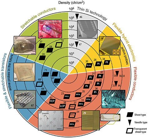
Figure 2. Development trends of flexible neural interfaces and electrode density in terms of the level of technological proficiency (see the text for an explanation). The flexible neural interfaces use a variety of substrates: polyimide (PI), Parylene (PPX), poly lactic-co-glycolic acid (PLGA), photoresist SU-8, liquid crystal polymer (LCP), or fluorinated ethylene propylene (FEP). Reprinted with permission from [27, 29, 32–34, 37, 46, 67, 68]. Filled symbols represent opaque probes of the sheet or needle type. Unfilled symbols represent transparent probes of the sheet-type.
Download figure:
Standard image High-resolution image2.3. Techniques for high-density multichannel microelectrodes
In figure 3, the electrode density is mapped against the number of electrodes for current flexible neural interfaces. As a representative example of multichannel electrodes using photolithography, we analyze the 96-channel flexible neural interface developed by Kaiju et al [31]. They prepared cortical ECoG electrodes with 96 measurement points, with a distance of 700 µm between measurement points, and thicknesses of 20 µm, using PPX-C as the base material (figure 4(a)). The flexibility enabled electrode placement not only on the cortex surface but also in the central sulcus (Rolandic fissure, figure 4(b)). ECoG recordings from anesthetized monkeys under electric stimulation on individual fingers allowed a high-resolution map of activity on the somatosensory cortex to be obtained (figure 4(c)). Furthermore, measured ECoG signals showed that the stimulated fingers can be estimated with an accuracy of approximately 98%. This study has demonstrated the feasibility of electrode miniaturization.
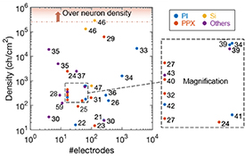
Figure 3. Electrode density according to number of electrodes. The electrodes are color-coded depending on which substrates they were fabricated on: PI, PPX, Si, and others (silicone [28, 37, 59], PLGA [30], SU-8 [35], LCP [39], and FEP [43]).
Download figure:
Standard image High-resolution image
Figure 4. Flexible ECoG electrode array. (a) Photograph of fabricated ECoG electrode array. (b) Intraoperative photograph of array placement on somatosensory cortex of a monkey (CS, central sulcus; IPS, intraparietal sulcus; A, anterior; P, posterior; M, medial; L, lateral). The central sulcus was partially unfolded, and arrays were inserted into it. (c) Distribution of somatosensory evoked potentials during digit stimulation (stimulus intensities of 1 and 4 mA). The surface potential 18 ms after digit stimulation is color-coded and presented. Reprinted with permission from [31].
Download figure:
Standard image High-resolution imageThe number of channels is typically limited up to a few hundred per square centimeter for passive electrodes (i.e. electrodes without active components, figure 3). The number of wired connections rapidly increases, reducing the available area as more channels are included. Consequently, integration technology should become more sophisticated and miniaturized for individual microelectrodes (measurement points) to fit the required amplifiers and analog-to-digital converters. To further increase the number of channels in neural interfaces, Musk et al simultaneously developed flexible electrodes and an application-specific integrated circuit for signal processing [33]. They used ∼4 μm thick PI substrates to fabricate a high-density flexible neural interface to be implanted in the brain. The integrated circuit was mounted using flip-chip bonding, reaching an electrode density of 21 114 channels cm–2 and implementing 3072 channels (the upper level of flexible electronics as shown in figure 2).
Another approach uses an active electrode array with a switching transistor on each electrode to reduce the number of connections. Chiang et al developed an active electrode array with an electrode density of 1212 channels cm–2 and 1008 channels using thin Si semiconductors on a PI substrate (the upper level of flexible hybrid electronics as shown in figure 2) [34]. With an active matrix using flexible hybrid electronics, the same number of connections for 1008 (36 × 28) passive electrodes is omitted. The number of connections reduces to 92 (28 × 2 + 36) in this circuit design. To dramatically increase the number of channels, flexible transistors that are either bendable or stretchable have been developed using carbon nanotubes and organic semiconductors [67–71]. Although these transistors have not been implemented as a switching device in neural interfaces to date, their use in active electrodes is expected in the future. Wang et al achieved a transistor array with 6300 channels and a density of 325 channels cm−2 using carbon nanotubes (upper level of flexible organic transistors as shown in figure 2) [68].
The design of multichannel systems depends on the switching speed of the active electrodes (transit frequency is determined by mobility and channel length) [48], the multiplexing performance of the measurement device, and the number of channels that can be simultaneously registered. Still, the processing technology using flexible transistors must be advanced to achieve higher density.
3. Reducing contact impedance for microelectrode miniaturization and small potential acquisition
The amplitude of brain activity acquired by methods such as ECoG and EEG is typically around 1–100 µV at 1–200 Hz, and spike signals (nerve impulses) are sub-millivolt at ∼10 kHz, while other biological potentials, such as those reflected in electrocardiography and electromyography, generate potentials up to a few millivolts at 1–400 Hz [3, 10, 21, 23, 66, 72–75]. The potential variations from brain activity are very small and cover a wide frequency range. Hence, conductive and semiconducting materials for neural interfaces should have low internal noise and robustness against external noise, such as hum noise or motion artifacts [3, 23, 35, 52, 66, 74, 76, 77].
The contact impedance of microelectrodes with the brain tissue increases as their area decreases. High contact impedance increases the susceptibility to external noise, hindering accurate potential measurements, especially above the permissible source impedance of the measurement device. Recent developments in Si circuits have enabled low-noise measurements over a wide frequency range of 1–1000 Hz and for a high permissible source impedance up to few megaohms [75, 78, 79]. When stretchable conductors are integrated for wiring in neural interfaces [28, 32, 37, 44, 56, 59], the permissible signal source impedance must consider the contact and wiring impedances, with the latter usually changing under strain. For stretchable conductors, whose integration technology can be further improved (figure 2), impedance matching with initial impedance and impedance under strain must be considered with respect to the measurement device to acquire the small potentials from brain activity.
In recent years, the contact impedance of microelectrodes has been dramatically reduced by the use of conductive polymers such as poly(3,4-ethylenedioxythiophene)-poly(styrenesulfonate) (PEDOT:PSS) (figures 5 and 6). As shown in figure 5, the use of PEDOT:PSS achieves normalized contact impedance (i.e. impedance multiplied by the area contacting a liquid) of 0.024–0.12 Ω cm2 at 1 kHz [29, 33], being at least two orders of magnitude lower than that of common materials for microelectrodes, such as gold (Au) (0.3–41 Ω cm2), platinum (Pt) (1.5–950 Ω cm2), Pt black (0.25–0.26 Ω cm2), graphene and carbon fiber (18–100 Ω cm2), IrOx (3.1–57 Ω cm2), Si (63–42 000 Ω cm2), and gel (1.1 Ω cm2). PEDOT:PSS proves particularly suitable for neural interfaces and corresponding bioelectronic applications, when considering its mixed electronic and ionic conductivity [29]. While neuronal signals are based on ionic currents, the coupling with electron-conducting, metal-based probes remains one of the major challenges for detecting high-quality signals. As ions can penetrate the bulky surface of the polymer, a direct influence on the polymer doping is enabled, and an improved interaction between the systems is given, when PEDOT:PSS is used as a surface coating (figure 6). Such interfaces can show miniaturized electrode arrays with high density while maintaining high signal quality at the same time. Therefore, microelectrodes based on PEDOT:PSS have enabled miniaturization and high density (21 114–62 500 channels cm–2) [29, 33].
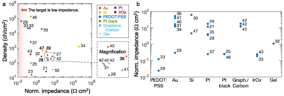
Figure 5. Solution-contact impedance. (a) Relation with electrode density. (b) Classification with electrode materials.
Download figure:
Standard image High-resolution image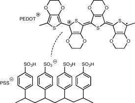
Figure 6. Chemical structure of PEDOT:PSS. The dopant PSS oxidizes PEDOT and thereby enables hole conductance along the π-backbone of the polymer.
Download figure:
Standard image High-resolution imageCurrent neural interfaces do not reach the targeted neuron density of 250 000 channels cm–2( figure 2). Hence, research on microelectrodes for direct and detailed brain activity monitoring continues pursuing higher densities and the integration of more channels.
4. Are thinner implants better for long-term in vivo brain activity monitoring?
Biocompatible polymers (e.g. PI, PPX, SU-8) [56, 80] have been widely used since the 2000s as substrates and encapsulants of flexible neural interfaces. These polymers have been thinned down to the order of several micrometers to increase flexibility. A total thickness of approximately 1 µm has been achieved using SU-8 to construct a neural interface for long-term implantation (∼4 months) [35]. A 3 μm thick PPX substrate (with a total thickness of 20 μm) has been used for implantation for up to 5 months [32]. A higher durability of 1–5 years has been achieved for thicker needle electrodes with a diameter of 30 μm and PI encapsulation as well as for PI used in encapsulation and with substrates with thicknesses of 12.5 μm each [34, 81]. The long-term robustness of flexible neural interfaces is being increasingly reported (figure 7).
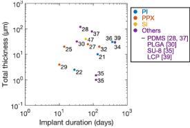
Figure 7. Total thickness versus duration for long-term implantation.
Download figure:
Standard image High-resolution imageThere may be a tradeoff between robustness and film thinness. The selection criteria for substrates and encapsulants are gas permeability and water uptake for the wiring and electronic devices (for protection against moisture and ions). Gas permeability is inversely proportional to thickness, and the gas permeability of a polymer is four orders of magnitude higher than that of metals and ceramics (figure 8) [54]. Regarding water uptake, PI has a value of 0.8%, while PPX and SU-8 show absorption of less than 0.06% [55, 56]. Even with high gas permeability and water uptake, polymers have shown excellent long-term durability in vitro[ 82–85]. However, damage to polymer-based insulation has been observed in vivo on the chemical elements, electrical impedance, and dielectric constant [82, 86]. This does not occur only in polymers. Hämmerle et al reported that a thermally grown silicon-dioxide dielectric layer remained unchanged after 21 months in vitro, but was etched in vivo after only 10 months, leading to implantable device failure [87]. In fact, the evaluation of in vivo implementations demonstrates a completely different degradation behavior to in vitro experiments, with the former presenting signal crosstalk between connections on thin polymer substrates as a result of the reduced insulation resistance and the increased capacitance with the accelerated reduction of wiring space [88, 89]. In addition, gas permeability affects devices that are susceptible to moisture-induced property changes [90–92].

Figure 8. Material permeability as a function of thickness. The duration scale shows the approximate time required for water vapor to pass through a layer of material such that the humidity inside the package is 50% of the external humidity. Reprinted with permission from [54].
Download figure:
Standard image High-resolution imagePinholes also have a great impact on films. Unlike the processes used to produce PI and SU-8 by spin-coating and curing precursors, PPX films are coated by gas-phase growth. According to Pierstorff et al [93], when deposited in the range of a few microns in thickness, pinholes appear in the PPX coating, and when further thinned to 40–300 nm, the coating becomes porous and leaches proteins and other materials. This thinning process substantially reduces the gas and water permeability and makes films more prone to mechanical tearing [56]. Therefore, thinning the substrate may compromise the robustness of a neural interface. The relation between thinness and robustness, as understood from figure 7, will become clearer as more attempts at long-term implantation are made.
We suggest various methods to address the tradeoff between robustness and thinness of films properly. Pretreatment of the coating object, such as plasma treatment, before the PPX gas-phase growth, leads to the formation of dense thin PPX films with thicknesses below 1 μm [94]. Novel encapsulants and substrates to reduce gas permeability and water uptake, such as organic/inorganic multilayer thin-film structures [90, 91], will be needed for long-term studies to prevent crosstalk and protect embedded devices that are susceptible to moisture-induced property changes. For SU-8, long-term durability cannot be easily achieved, but manufacturing optimization may increase the likelihood of obtaining long-term durability [83]. Continued efforts to achieve robust thin films are necessary. Meanwhile, polymer degradation should be evaluated in vivo or in an aging environment, such as phosphate-buffered saline solution with added hydrogen peroxide or potassium chloride [82, 86, 95] to evaluate the long-term robustness of flexible neural interfaces.
Reliable and safe materials and structures remain crucial for developing substrates and encapsulants in flexible neural interfaces with the ambition of implantation over periods of years.
5. Multifunctional neural interfaces
The development trends for flexible neural interfaces mostly focus on high-density multichannel microelectrodes with high durability. Recently, we developed a neural interface with stretchability, optical transparency, easy intraoperative handling, and high durability [32, 72, 96]. In this section, we analyze multifunctional conductive materials for connections and various application technologies.
Novel conductive materials that are intrinsically stretchable and transparent, such as carbon nanotubes, graphene, conductive polymers, and metal nanowires, have been used to develop transparent conductors (figure 9(a)). For instance, silver (Ag) nanowire films enable miniaturization due to their metallic nature and high electrical conductivity. Nanowires randomly establish mesh networks in-plane to form conductive passes, resulting in optical transmittance under light penetration through the openings between nanowires (figure 9(b)). Orientation control, such as cross-alignment with Ag nanowires, can establish efficient network paths (figure 9(c)) [96]. In figure 9(a), it is shown that cross-aligned Ag nanowires reach the most transparent conductors with a width of approximately 20 µm, a sheet resistance of 25 Ω sq–1, and a light transmission of 96% . In addition, Ag nanowires can be made stretchable on elastomer substrates by special treatments. For example, Au nano-plated Ag nanowire (e.g. Ag/Au core–shell nanowire) interconnections have shown stretching resistance over 100 cycles under 20%–60% strain (figure 9(d)) [72].
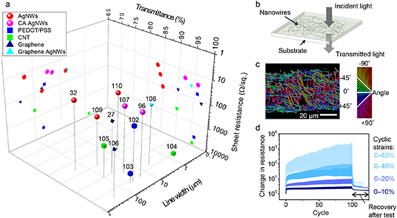
Figure 9. Characteristics of transparent flexible conductors. (a) Relation between sheet resistance, optical transmittance at a wavelength of 550 nm, and line width for Ag nanowires (AgNWs), cross aligned AgNWs (CA AgNWs), PEDOT:PSS, carbon nanotubes (CNTs), graphene, and hybrid graphene–AgNW. (b) Schematic diagram of AgNW-based transparent flexible conductor. (c) External view of CA-AgNWs. (d) Stretchability of AgNWs. Reprinted with permission from [32, 72, 96].
Download figure:
Standard image High-resolution imageA flexible neural interface has been developed using stretchable and transparent wirings made of Ag/Au core–shell nanowires (figure 10(a)). The neural interface consists of 16 channels for brain surface recordings using PPX encapsulation and a substrate with total thickness of 5 μm. The surface of the neural interface is treated with antithrombogenic (i.e. blood compatible) polymer and incorporates a vital warmth deformable polymer. The antithrombogenic polymer effectively inhibits granulation tissue formation, which is typically induced by biological foreign body reaction [18, 97, 98] and increases the separation between the brain tissue and microelectrodes. The deformable polymer is hard at room temperature intraoperatively but softens and becomes transparent by the body temperature of the brain surface. Therefore, the neural interface does not flutter while in air and can be easily placed in the desired brain surface position. The ion migration resistance of the Ag nanowires is improved by using Au nano-plating to form a shell. The neural interface does not degrade during immersion in saline solution for more than 5 months. The use of polyvinyl alcohol-based gel as a microelectrode also promotes durability and enables soft attachment due to its low Young's modulus of 70–400 kPa [99, 100].

Figure 10. Multifunctional neural interface. (a) Schematic of a neural interface that is flexible, transparent, durable, and has easy intraoperative handling. (b) Diagram of a long-term implantation study on rats. (c) ECoG recordings from anesthetized rats. (d) General view of neural interface and optogenetic study with micro-LED. Brain activity in ECoG was elicited by light. Reprinted with permission from [32, 72].
Download figure:
Standard image High-resolution image
The long-term stability of ECoG signal acquisition on the dura mater has been confirmed from somatosensory evoked potentials. Normally, SEP is observed as a potential deflection of the cortical surface with the typical latency after sensory stimulation (figure 10(b)). This response allows the evaluation of the reliability of signal acquisition. The intensity of somatosensory evoked potentials was considerably attenuated after several weeks of in vivo implantation without the antithrombogenic polymer. In contrast, the developed neural interface acquired consistent somatosensory evoked potentials after 2 months of implantation in rats (figure 10(c)). The growth of granulation tissue was prevented after 5 months of implantation. Furthermore, optogenetics has been expressed in the marmoset brain to record neural activity using the developed neural interface. The transparency of the neural interface has allowed optical stimulation with few blind spots, and neural responses to blue laser or LED light stimulation have been recorded with low noise (figure 10(d)).
6. Summary
This review focuses on flexible neural interfaces considering the softness of brain tissue. We summarize development trends in terms of electrode density, number of electrodes, electrode impedance, total thickness, and durability of electrode arrays. High density in microelectrode arrays enables the achievement of a high signal-to-noise ratio provided that the contact impedance between the brain surface and electrodes is within the permissible source impedance of the measurement device. High-density microelectrode arrays allow the measurement of detailed brain activity and increases the accuracy of brain state estimation.
Microelectrode miniaturization is inversely proportional to the solution-contact impedance. Conductive polymers are important for decreasing the impedance as a result of their low impedance of ∼0.024 Ω cm2 at 1 kHz compared with the widely used Au, Pt, and Pt black, with impedances of ∼0.25 Ω cm2. Each electrode requires switching transistors to build an active matrix and prevent a drastic increase in the number of wired connections as more measurement points are integrated. Currently, 1008 active electrodes have been integrated on a polymer substrate using thin Si semiconductors. Meanwhile, intrinsically flexible transistors (e.g. single-walled carbon nanotubes and organic transistors) are also suitable as active electrodes. Neural interface operation depends on the switching frequency of the active electrodes and the performance of the related devices.
The use of thinner substrates and encapsulants to increase the flexibility of neural interfaces may lead to a tradeoff with long-term robustness. Therefore, breakthroughs in materials and structures are required to simultaneously minimize brain invasiveness and achieve long-term implantability for advancing multifunctional neural interfaces. Multifunctional neural interfaces with versatile bending robustness, high density, long-term durability, stretchability, transparency, and easy intraoperative handling may be achieved by using metal nanowires. Such neural interfaces can enable simultaneous ECoG recordings and optogenetic stimulation.
The assessment of device durability needs to be performed with attention to different degradation behaviors between in vivo and in vitro experiments. As mentioned before, the important factors are gas permeability and water uptake. In addition, implant device failure may occur as a result of the degradation of biomaterials caused by phagocytes such as adherent macrophages and foreign body giant cells in the foreign body reaction [98]. Although a unified evaluation method is preferable for device durability, various evaluation methods have been proposed for different purposes in vitro. Simulated body fluids, sterile urine, and bacteria inoculated media are used for in vitro testing [82, 86, 95, 101]. The long-term robustness of flexible neural interfaces will ultimately be required if a device such as a brain-machine-interface is to assist with bodily functions for a lifetime.
The measurement and control of neural activity can establish a closed-loop system for applications such as the brain–machine interfaces to assist physically disabled people and promote neuroplasticity. For instance, high-density flexible neural interfaces, such as those analyzed in this paper, will be indispensable for brain–machine interfaces that enable accurate control of a robot manipulator, including its fingers. Furthermore, if a neural interface with a density comparable to that of neurons and a sufficient number of electrodes is realized, high trial reproducibility can be achieved, opening new frontiers in the measurement of brain functions.
6.1. Density calculation
In order to enable a straightforward comparison, electrode densities have been calculated based on the given data of each publication. Where values were not given in the text, array dimensions were extracted from figures. In general, this review has considered the best possible outcome of any publication with respect to its achieved properties. With respect to different array designs, further simplifications and conversions needed to be made in some cases. An outline follows.
If not provided by the authors, densities have been calculated based on electrode pitches, which should increase uniformity. If multiple densities were present, e.g. due to varying spacings, densities were usually calculated based on the best data available. In cases where pitches and spacings were not given, densities are based on the channel number in the covered area. Pitches are defined as electrode distances from center-to-center, whereas interelectrode spacings are defined as edge-to-edge.
Acknowledgments
This study was supported by the Murata Science Foundation, by the Center of Innovation Program of the Japan Science and Technology Agency (JST), by the Japan Society for the Promotion of Science (JSPS) KAKENHI, by FrontierLab@OsakaU of Osaka University, by the New Energy and Industrial Technology Development Organization (NEDO), by the Japan Agency for Medical Research and Development (AMED), and by the Commissioned Research of National Institute of Information and Communications Technology (NICT).