


Abstract
We fabricated non-volatile resistive memory devices on a commercially available flexible paper substrate using physical vapor deposition methods in all of the fabrication steps. By using only evaporable component materials including aluminum oxide (Al2O3) and metal electrodes, it has become possible to constitute the vertical stacking Al2O3 active layer structure with metal electrodes in the memory devices without wet or crumpled damage on the paper substrate. The memory devices showed the typical unipolar switching characteristic with excellent electrical performances of low operating threshold voltage (∼3.2 V), high ON/OFF ratio (∼104), good reproducibility (∼500 endurance cycles), and stability (∼104 s of retention times). The outstanding flexibility of the paper substrate has made it possible to stably maintain the electrical properties of the memory devices both in flat and bent configurations (radius of 5 and 1 mm) without any serious degradation.
Export citation and abstract BibTeX RIS
1. Introduction
Research and development of paper-based electronic devices have been widely carried out in recent years to achieve a novel technology for portable electronic products, which have challenging advantages for the future of the electronic industry such as low cost, light-weight, flexibility, and easily recyclable properties [1–3]. Paper is well-known for its interesting attributes. First of all, it is one of the most ubiquitous materials for widespread utilization in human society, and it is made from common woods, that is, it can be supplied from nature almost unlimitedly. In addition, paper can be easily recycled and is disposable compared to other nearly indecomposable substrates made from plastic materials, highlighting its eco-friendly properties. Although paper has been mainly used for primary storage media such as books, it is now being considered as a potential substrate for the next generation of electronic devices of flexible digital media. Because paper has intrinsic insulating behavior due to the material properties of the cellulosic fiber, it can be applied as a substrate for electronic devices without any additional layer coating. Low temperature physical vapor deposition processes are also available as in the case of other flexible plastic substrates [2–6]. Recently, research of electronic devices on paper substrates are being widely conducted in the fields of transistors [4–8], memories [9], circuits [10–12], solar cells [13], fluidic chips [14], active matrix displays [15], electroluminescence devices [16], bioassays [17], and touch pads [18]. Similar to research studies on paper substrates for electronic devices, the field of inorganic memory devices has been consistently developed for their outstanding electrical performance, material variety, and fabrication diversity, including evaporation methods [19–22]. Furthermore, the series of metal-oxide inorganic materials used for the thin active layer of the memory devices also have sufficient flexibility to be used as constituents of electronic devices on a flexible substrate, and therefore can be actualized to make non-volatile memory devices using only evaporable inorganic materials on the paper substrates [23].
In this study, we fabricated non-volatile memory devices on a paper substrate using only evaporable component materials by physical vapor deposition methods. For the active layer of resistive memory devices, the vertical stacking layer structure composed of aluminum oxide (Al2O3) and Au materials was used with Au (top) and Al (bottom) electrodes. The fabricated memory devices exhibited a typical unipolar switching characteristic with good electrical performance, such as reliability and stability. The outstanding flexibility of the paper substrate enabled the electrical properties of the memory devices to be preserved in bent configurations (radius of 5 and 1 mm) without any serious degradation.
2. Experimental methods
Figure 1(a) shows the photographic images of the paper substrate used in this study. The paper substrate is a common wrapping paper used for presents (purchased from Coco Inc., Korea). Figure 1(b) exhibits the schematic illustration, photographic, and optical microscopic images of the memory devices on the paper substrate, respectively. To fabricate the devices, firstly, a large paper sheet was cut into pieces of appropriate size (1.5 × 1.5 cm2) to be used as substrates. The paper substrate was cleaned by dipping into the isopropyl alcohol for a 1 min, followed by a drying process in a thermal oven at 80 °C overnight to remove the residual solvent and moisture on the substrate (figure 1(a)). The bottom electrodes (Ti/Au/Al = 10/100/50 nm) were widely deposited on the center region of the paper substrate by an electron beam evaporator (for Ti/Au) and thermal evaporator (for Al) with a deposition rate of 0.5 Å s−1 at a pressure of ∼10−7 torr. The active layer and the top electrodes (Al2O3/Au/Al2O3/Au = 30/20/30/50 nm) were deposited with an 800 μm-diameter circular patterned shadow mask using the electron beam evaporator with the same deposition conditions (figure 1(b)). Figure 2(a) shows the cross-sectional transmission electron microscopy (TEM) image along the vertical stacking layer device structure, and figures 2(b) to (e) show the density of specified elements described by the brightness of selected colors in the same region as the TEM image. Because the Al element is also included in the active Al2O3 layers, the orange color (figure 2(b)) of Al appeared not only in the bottom Al electrode but also in the active Al2O3 layers with a slightly dimmer color compared to that in the bottom Al electrode which contained only the Al element. As we used Au material in the top and bottom electrodes and the active layer was surrounded with Al2O3 layers, the red color (figure 2(c)) of Au distinctly appeared to be divided without any intersection in the Al2O3 layers. The green color (figure 2(d)) of oxygen appeared to be bright mainly in the Al2O3 layers, and the Pt material represented by the purple color (figure 2(e)) was used as a protection layer to prevent physical damage to the device structure during focused ion beam processing for making the TEM sample.

Figure 1. (a) Photographic images of the diced and cleaned paper substrate from a large wrapping paper sheet. (b) The schematic illustration, photographic, and optical microscopic images of the memory devices.
Download figure:
Standard image High-resolution image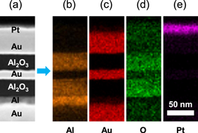
Figure 2. (a) Cross-sectional TEM image and (b)–(e) specified element profile mapping along the vertical stacking layer device structure.
Download figure:
Standard image High-resolution image3. Results and discussion
Figure 3(a) shows the representative current–voltage curve of the memory devices on the paper substrate. To switch on the memory devices from the initial high resistive state (OFF state) to the low resistive state (ON state), we applied a dual sweep voltage from 0 to 4 V (black line). In the forward voltage sweep from 0 to 4 V, the current value remained low (OFF state) in the low voltage region, but it abruptly increased when the voltage reached ∼3.2 V, indicating memory switching to the ON state. The increased high current value was still retained in a backward voltage sweep from 4 to 0 V, and maintained even in the low voltage region of the second single sweep from 0 to 6 V (red line) after finishing the first dual sweep voltage, indicating the non-volatility of the memory devices. The ON state current decreased when the voltage reached ∼2.5 V during the second single sweep, showing negative differential resistance (NDR) behavior, which enables the memory devices to have rewritable switching characteristics with potential applicability as future memory devices. The inset plot shows the ON/OFF ratio as a function of the voltage. At a reading voltage of 0.3 V, the ON/OFF ratio reached ∼104 with a large memory window. The electrical resistive switching of the memory devices' accompanying NDR behavior can be interpreted in terms of a space charge accumulation phenomenon caused by excess charge injection. When the external bias voltage is applied to the electrode, the injected charges get continuously accumulated and build up the charge injection barrier between the active layer (organic or inorganic) and electrode, forming the NDR region. The current decreases with the bias voltage because carrier injection is inhibited with a highly localized internal electric field from the accumulated space charge after trap filling [24–28]. Figure 3(b) shows a double-log plot analysis of the memory devices. Here, the space charge limited current (SCLC) conduction behavior was also observed with a slope of ∼2.0 in the OFF state region, indicating correspondence with the formation mechanism of the NDR region. But in the ON state region, the slope was found to be ∼1.3, which suggested the possibility of another mechanism like Poole–Frenkel conduction, rather than ohmic or SCLC conduction [29]. As shown in figure 3(c), the linear characteristics of the current were uniformly observed in log (I/V) versus V1/2 plot analysis, indicating that the Poole–Frenkel emission can be the dominant charge transport mechanism in the ON state [30]. As outlined above, an initially injected charge carrier begins to form a percolation path gradually with the trap filling process based on the classical SCLC model, and when the high electric field is induced with a threshold voltage regime, part of the shallowly-trapped charge can be reemitted with rapidly increased state current to be a low resistive state, exhibiting Poole–Frenkel conduction behavior [30–32]. Of course, the additional excess charge cannot help leading to space charge accumulation with NDR behavior. For the bi-stable resistive memory devices, it can be also important to check the material stability of the Al2O3 layer as the insulating property because there should be no leakage current through the resistive layer before forming the intended percolation current path. As shown in figure 3(d), the Fowler–Nordheim tunneling effect was not observed in log (I/V2) versus 1/V plot analysis, confirming the good insulating property of the thin Al2O3 layer [33]. By using this Al2O3 material as a constituent layer, several types of resistive memory devices have been researched recently [34, 35], especially focusing on the multi-junction Al2O3 active layer structure to improve the endurable reproducibility of the memory devices by increasing the effective number of localized active regions before permanent dielectric breakdown would occur in all of the Al2O3 layer [35].
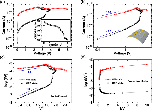
Figure 3. (a) The current–voltage curve of the memory devices. The inset shows the ON/OFF ratio as a function of the voltage. (b) A double-log plot analysis of the current–voltage characteristics. (c) log (I/V) versus V1/2 plot for Poole–Frenkel analysis and (d) log (I/V2) versus 1/V plot for Fowler–Nordheim analysis.
Download figure:
Standard image High-resolution imageTo examine the reliability of the memory devices, we performed statistical analysis of the measured electrical data of the memory devices. Figure 4(a) shows the statistical distribution of the threshold voltage in 36 operating memory cells of the devices in the flat condition. The memory switching to the ON state was mainly observed at ∼3.2 V with a narrow range of deviation within approximately 0.8 V, indicating good statistical uniformity of the memory devices. Figures 4(b) and (c) show the same plots in the bent configurations with a radius of 5 and 1 mm, respectively. Here, the statistical properties as the peak points and deviations were similarly maintained as in the flat configuration. Figures 4(d) to (f) exhibit the cumulative probability of each resistive state of the memory devices at the reading voltage of 0.3 V in the flat and bent configurations with a radius of 5 and 1 mm, respectively. The ON and OFF state currents were initially separated at least by two orders of magnitude, which is a sufficient value for confirming the bi-stability of the resistive memory devices. Although the ON state currents were slightly decreased by physical strain damage onto the active layer as the bent radius was reduced to 1 mm, significant electrical changes were mostly not observed in each resistive state, indicating the statistical reliability of the memory devices. We also characterized the endurance cycles and retention properties of the memory devices. Figure 5(a) shows the DC sweep endurance test of the memory devices in the flat condition. The endurance property was measured from repetitively switching the device ON and OFF in the DC sweep test of a single memory device cell. During ∼500 cycles of the repetitive sweeps, the currents of each resistive state measured at the reading voltage of 0.3 V were well preserved (ON currents of ∼10−4 A, and OFF currents of ∼10−8 A), maintaining an ON/OFF ratio of ∼104 without serious fluctuation. Figures 5(b) and (c) show the same plots in the bent configurations with a radius of 5 and 1 mm, respectively. Overall, the repetitive endurance properties were well maintained in each configuration except in the bent radius of 1 mm where a little degradation appeared on bi-stability and repetitiveness from the extreme bent strain effect on the devices [36–38]. Figures 5(d) to (f) show the retention tests of the memory devices in the flat and bent configurations with a radius of 5 and 1 mm, respectively. The currents of each resistive state were observed at the reading voltage of 0.3 V with a reading interval of 50 s, and they were stably maintained for ∼104 s of retention time, indicating not only reproducibility but also stability of the resistive memory devices in practical flexible conditions.

Figure 4. The threshold voltage distribution of the memory devices in the (a) flat and bent configurations with a radius of (b) 5 and (c) 1 mm. The cumulative probability of the memory device in the (d) flat and bent configurations with a radius of (e) 5 and (f) 1 mm.
Download figure:
Standard image High-resolution image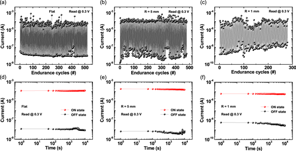
Figure 5. DC sweep endurance test at a voltage of 0.3 V in the (a) flat and bent configurations with a radius of (b) 5 and (c) 1 mm. The retention tests of each resistive state for about 104 s at a voltage of 0.3 V with a reading interval of 50 s in the (d) flat and bent configurations with a radius of (e) 5 and (f) 1 mm.
Download figure:
Standard image High-resolution image
4. Conclusion
In summary, we fabricated non-volatile memory devices on a commercially available wrapping paper substrate by using physical vapor deposition methods in all of the fabrication steps. In the fabrication processes, we constituted the vertical stacking device structure composed of Al2O3 and Au materials as the active layer with Au (top) and Al (bottom) electrodes, and they showed a typical unipolar switching characteristic with outstanding electrical performance of low operating threshold voltage (∼3.2 V), high ON/OFF ratio (∼104), good reproducibility as repetitive endurance property (∼500 cycles), and stability as retention property (∼104 s). The resistive switching characteristics of the memory devices has been explained with the SCLC and Poole–Frenkel conduction mechanism, ensured by the linear properties of the state currents in the double-log plot analysis. The outstanding flexibility of the paper substrate has made it possible to stably maintain the electrical properties of the memory devices both in flat and bent configurations (radius of 5 and 1 mm) without any serious degradation.
Acknowledgments
The authors appreciate the financial support of the National Creative Research Laboratory program (Grant No. 2012026372) through the National Research Foundation of Korea (NRF), which is funded by the Korean Ministry of Science, ICT & Future Planning, and the Research Institute of Advanced Materials (RIAM) of Seoul National University.