

Abstract
To guide the illuminating design to improve the on-state performances of gallium arsenide (GaAs) photoconductive semiconductor switch (PCSS), the effect of spot size on the operation mode of GaAs PCSS based on a semi-insulating wafer with a thickness of 1 mm, triggered by a 1064-nm extrinsic laser beam with the rectangular spot, has been investigated experimentally. It is found that the variation of the spot size in length and width can act on the different parts of the output waveform integrating the characteristics of the linear and nonlinear modes, and then significantly boosts the PCSS toward different operation modes. On this basis, a two-channel model containing the active and passive parts is introduced to interpret the relevant influencing mechanisms. Results indicate that the increased spot length can peak the amplitude of static domains in the active part to enhance the development of the nonlinear switching, while the extended spot width can change the distribution of photogenerated carriers on both parts to facilitate the linear switching and weaken the nonlinear switching, which have been proved by comparing the domain evolutions under different spot sizes.
Export citation and abstract BibTeX RIS
1. Introduction
Gallium arsenide (GaAs) photoconductive semiconductor switch (PCSS) is a new type of solid-state device, that combines ultrafast laser with photoelectric semiconductor [1‒3]. As one of the most promising high-power closing switches, it has drawn wide attention in the fields of high-power microwave generation and pulsed power technology, due to its many inherent advantages such as ultrafast switching, high power, low time jitter and compact structure [4‒6].
According to the number of electron-hole pairs induced by each absorbed photon and the features of the output waveform via the switch, the operation mode of GaAs PCSS can be classified as linear or nonlinear mode [7]. For the linear mode, the generation of carriers almost all depends on the incident laser pulse, and the output pulse width is approximately same as that of the incident laser pulse. Operating in this mode, the switch presents the characteristics of lower jitter and long lifetime, but usually needs the ~ mJ level laser energy for the high power output. Compared to the linear mode, the PCSS in the nonlinear mode can remain in the turn-on state after the laser is extinguished, making the output pulse width reach tens of nanoseconds, or even hundreds of nanoseconds and above [8‒10]. The switch operating in this mode features the avalanche multiplication of carriers. The energy for the carrier gain is from the high bias electric field (> 4 kV/cm) and powerful impact ionization. A weak light from ~ nJ level to ~ μJ level is usually enough to trigger the GaAs PCSS to the conduction state, which significantly reduces the weight and volume of the required laser and makes the PCSS of great value in constructing compact pulsed power systems [11, 12]. It is worth noting, no matter what mode the switch is operating in, under the same triggering and bias conditions, improving the on-state performances, such as photoelectric conversion efficiency and triggering efficiency, to obtain higher output on the load, is highly significant for the application of GaAs PCSS in high-power systems [13, 14].
Some studies have pointed out that the photoelectric conversion efficiency of linear PCSS can be significantly improved by adopting the illuminating spot with the appropriate profile or location [15, 16]. In addition, some typical illuminating spots with specific shapes have also been designed to characterize the influence of the spots on the photoelectric threshold and triggering efficiency of the PCSS operating in the nonlinear mode [17, 18]. Almost all existing researches indicate that the illuminating spot significantly affects the development of operation mode, further determining the on-state performances of PCSS. However, despite these efforts, the influencing mechanism of the spot size on the operation mode of GaAs PCSS is still unclear, especially when the PCSS employs the extrinsic photoconductivity, generally introducing the optical absorption depth of several millimeters and evoking the complex switching transient [9, 19]. Furthermore, to take full advantage of the illuminating laser and switch material, further investigating the influencing mechanism to optimize the illuminating spot and improve the on-state performances of GaAs PCSS is of considerable practical significance.
In this work, A coplanar semi-insulated (SI) GaAs PCSS with a 1-mm-thick GaAs wafer is triggered by the 1064-nm laser pulse. The output waveforms integrating the characteristics of the linear and nonlinear modes are obtained, and the effect of the size variation of a rectangular spot on the operation mode is investigated experimentally. On this basis, the physical model based on two equivalent current channels is introduced, and the domain evolutions under different spot sizes are comparatively analyzed, which reveals well the relevant influencing mechanisms.
2. Experimental setup
2.1. Device structure
A coplanar GaAs PCSS was fabricated and used in our tests. The device structure is represented in figure 1(a). The dark electrical resistivity and the electron mobility of the SI-GaAs wafer are ~ 5×10⁷ Ω·cm and ~ 8500 cm2/(V·s), respectively. The wafer size is 14 mm×6 mm×1 mm. The Au/Ge/Ni (200 nm/100 nm/100 nm) multilayer alloys were deposited on the surface of the SI-GaAs wafer by electron-beam evaporation, and then good ohmic contact between the electrode and the wafer was formed through rapid thermal annealing. The horizontal gap between the contacts is 5 mm. To avoid the thermal damage, the conductive silver adhesive curing at the temperature below 100 °C, was adopted to weld the copper foil, linking the PCSS to the external circuit. Furthermore, the GaAs PCSS was immersed into the transparent transformer oil to prevent surface flashover.
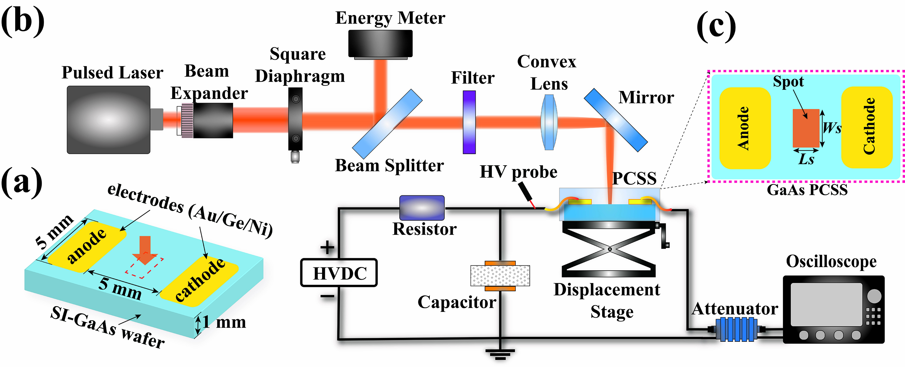
Fig. 1 Device structure and test circuit. (a) Schematic diagram of a coplanar GaAs PCSS. (b) Schematic of the experimental test circuit. (c) The layout of the rectangular spot illuminating on the GaAs PCSS.
Download figure:
Standard image2.2. Test circuit
The test circuit shown in figure 1(b) is set up to carry out the on-state test of the GaAs PCSS. A ceramic capacitor of 140 pF is charged by an adjustable high-voltage (HV) DC power supply via a 10-MΩ resistor, which provides the bias voltage (Vb) for GaAs PCSS. The laser used for triggering the PCSS is a 1064-nm Nd: YAG nanosecond laser with the full width at half-maximum (FWHM) of ~ 2 ns. In the triggering light path, the laser passes through a beam expander and a square diaphragm in sequence, and then is divided into two beams by a beam splitter. One beam is used to trigger the GaAs PCSS, after passing through a filter, a convex lens and a mirror. The other is monitored by an energy meter to determine the real-time illuminating energy (OE). In the experimental setup, the rectangular spot [in figure 1(c)] is adopted to illuminate the middle region of the GaAs PCSS. The spot size is measured by using an infrared sensor and a vernier caliper. The beam expander is added to make the spatial energy of the laser beam more uniform, to provide an approximately uniform spot for triggering the PCSS. The square diaphragm is used to adjust the spot size by controlling the uniform beam passing the aperture. Combining the square diaphragm and the displacement stage set below the PCSS, we can achieve the individual adjustment on the spot length (Ls) or width (Ws), under the case that OE is fixed. In the test, once the PCSS biased at Vb is triggered, the 140-pF capacitor discharges to the equivalent load of 50 Ω through the PCSS, during which the outputted electric pulse is attenuated in sequence by a high-voltage attenuator (30 dB/2 GHz/50 Ω, Huaxiang/SHX MS2-8000) and a conventional coaxial attenuator (40 dB/4 GHz/50 Ω), then recorded by a 500-MHz oscilloscope with a 50-Ω channel. A high-voltage probe (Tektronix P6015A) is used to measure the charging voltage across the ceramic capacitor to determine the bias voltage applied to the PCSS.
3. Experimental results
3.1. Influence of spot length on the output voltage
Under the condition that the bias voltage, triggering energy and the Ws are fixed, the output electric pulses under different Ls are first tested. Figure 2 shows the typical output waveforms of Ls = 2 mm, 3 mm, and 4.5 mm, under the case of Ws = 2 mm, Vb = 5.1 kV and OE = 103 μJ. It can be seen that the output waveforms cannot be simply classified as the outputs under the linear or nonlinear mode. On one hand, these waveforms present the characteristics of the linear mode, in which the rising edges are similar to that of the optical pulse. On the other hand, the apparent lock-on characteristics of the nonlinear mode also occur on the falling edge of these waveforms, to induce the wider pulse width than that of the optical pulse.

Fig. 2 Experimental optical pulse and typical output waveforms under (a) Ls = 2 mm, Ws = 2 mm, (b) Ls = 3 mm, Ws = 2 mm and (c) Ls = 4.5 mm, Ws = 2 mm. Here, the GaAs PCSS is biased at 5.1 kV and triggered by 103-μJ energy. The insets show the change of the spot length, and the gray area approximately frames the parts dominating the increase of the output amplitude.
Download figure:
Standard imageMore importantly, as the variation of spot length, the different evolution trends can be found in the output waveforms. When Ls increases from 2 mm to 4.5 mm, the falling edge of the output waveform uplifts gradually, forming a new peak (B), which will replace the previous peak (A) and dominate the increase of the output amplitude. The obvious double-peak characteristic can be observed under Ls = 3.0 mm, which indicates that the PCSS is operating in the transition from the linear mode to the nonlinear mode [20, 21], allowing us to analyze the evolution of the operation mode influenced by the variation of spot length. Here, the main part around peak A corresponds to the linear switching and the part around peak B corresponds to the nonlinear switching. From the evolution characteristics, we can find that the extension of the spot length along the current channel can enhance the development of nonlinear switching while restricting the development of linear switching.
3.2. Influence of spot width on the output voltage
Under the condition that the bias voltage, triggering energy and spot length are fixed, the output electric pulses under different spot widths are also tested. Figure 3 shows the typical output waveforms of Ws = 2 mm, 3 mm, and 4 mm, under the case of Ls = 1 mm, Vb = 4.5 kV and OE = 100 μJ. The obvious double-peak characteristics can also be found in the output waveforms under Ws = 2 mm or 3 mm. In these outputs, the parts around the first peak (C) are identical to the waveform of the optical pulse, which can be determined as the linear output. Interestingly, different from the evolution trend shown in figure 2, as the increase of spot width, the linear part of the output waveforms increases significantly and dominates the increase of the output amplitude. Pushed up by the increased linear part, the nonlinear part (around the peak D) also presents a slight increase when Ws increases to 3 mm from 2 mm, but when Ws is further widened, the nonlinear part is weakened obviously due to the stronger linear switching.
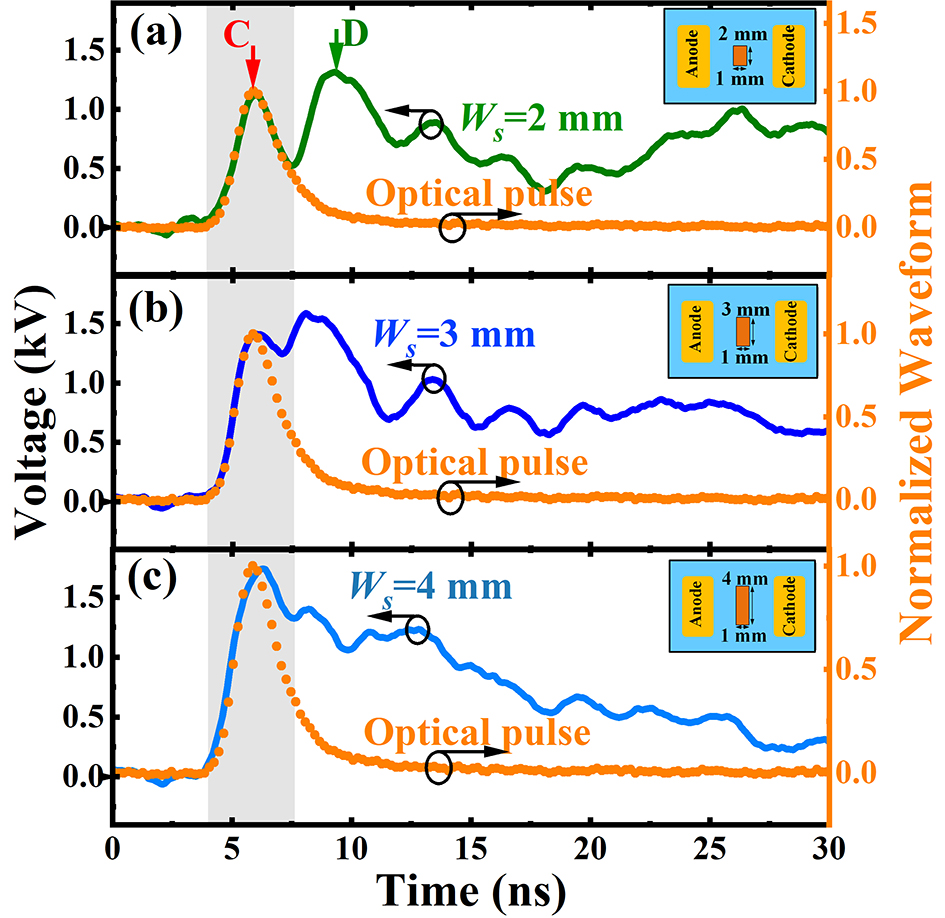
Fig. 3 Experimental optical pulse and typical output waveforms under (a) Ls = 1 mm, Ws = 2 mm, (b) Ls = 1 mm, Ws = 3 mm and (c) Ls = 1 mm, Ws = 4 mm. Here, the GaAs PCSS is biased at 4.5 kV and triggered by 100-μJ energy. The insets show the change of the spot width, and the gray area approximately frames the parts dominating the increase of the output amplitude.
Download figure:
Standard imageIt can be determined that the expansion of the spot width can induce a more significant enhancement on the linear switching, during which the output amplitude of the linear part can be approximately expressed as [22], Uout = (qvRL nc V)/l, where q is the unit of electric charge, v is the saturated velocity of carrier, RL is the load resistor, nc is the optically generated excess carrier density, V is the effective volume of the current channel, and l is the distance between two electrodes. For the same switch, the values of l, q, and v are approximately given. Considering the optical absorption mechanism of GaAs at 1064 nm [23], a higher triggering energy can excite more photogenerated carriers, inducing a higher nc V and Uout. Since the illuminating laser energy is kept as a constant in the experiment, we can infer that the increasing linear output with the increase of Ws is attributed to the more photogenerated carriers being assigned to participate in the linear switching.
3.3. On-state performances under the typical spots
Based on the above experimental results, it can be expected that a spot covering a large switching area can significantly enhance both linear and nonlinear switching. Thus, we compared the output waveforms under a small spot and a large spot approximately covering the whole switching area. The results are shown in figure 4. It can be seen that, compared to the small spot of 1×1 mm2, the large spot of 4.5×4.5 mm2 can induce a higher output. Here, a 1.9-fold improvement can be obtained, under Vb = 4.5 kV and OE = 100 μJ. Correspondingly, the voltage conversion efficiency increases to 39.8% from 21%. In our test, further improvement in the output voltage can also be achieved if we adopt a higher bias voltage or a larger triggering energy. Moreover, it is easy to find, when the spot is broadened from 1×1 mm to 4.5×4.5 mm, both of the evolution characteristics caused by the size variations in Ls and Ws are integrated into the output waveforms, from which the significant increase can be observed on the linear part (along trail E) as well as the nonlinear part (along trail F). This evolution trend is consistent with our above expectation.
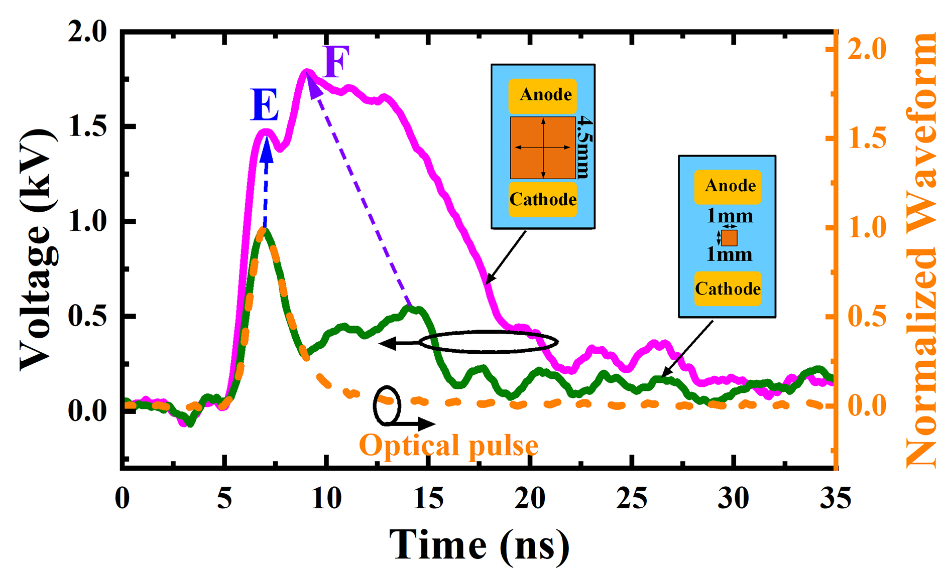
Fig. 4 Experimental optical pulse and typical output waveforms when the spot size is broadened from 1×1 mm2 to 4.5×4.5 mm2. Here, the GaAs PCSS is biased at 4.5 kV and triggered by 100-μJ energy. The insets show the spot sizes.
Download figure:
Standard imageIt is worth noting that the above experimental results can also match the existing reports about the effect of the typical spots on the on-state performances of GaAs PCSS. According to our results, the quasi-linear mode reported in references [19] and [24] can be well demonstrated. In this mode, compared to a line-shaped spot across the electrodes, a spot covering the whole switching area is adopted to obtain the higher photocurrent and suppress the current filament appearing on the nonlinear switching, contributing to the higher photoelectric conversion efficiency and device lifetime. For the GaAs PCSS operating in the nonlinear mode, as reported in [17], compared to the long-striped spot perpendicular to the current channel, the focused spot with a narrower spot width can induce a higher nonlinear-mode output. Additionally, similar to the results presented in reference [16], our results demonstrate that the line-shaped spot across the electrodes and the spot covering the whole switching area are more effective for inducing a higher output than the point spot or partial line-shaped spot.
4. Discussion
4.1. Equivalent channels participating in the switching
To gain insight into the physical mechanism of experimental results, the switching process of the GaAs PCSS operating in the transition from linear mode to nonlinear mode is first analyzed. Figure 5 depicts the physical diagrams of carrier dynamics during the switching. It is well known that the ultrafast switching of GaAs PCSS occurs on the filamentary current channel with a density of several MA/cm2 and an upper limit for the diameters ranging from 50 to 300 μm [8]. Prior to the appearance of the current filament, the delay stage of the switching transient always exists in the PCSS, and it is mainly a process that produces electron-hole pairs (photogenerated carriers) [25]. As shown in figure 5(a), an initial distribution of carriers is produced upon the optical excitation, and is concentrated in an area covered by the spot. Under the force of the applied electric field, the carriers move separately toward the anode and cathode, forming the photogenerated current. The current has a linear relationship with the incident optical intensity, presenting the linear-switching characteristics.
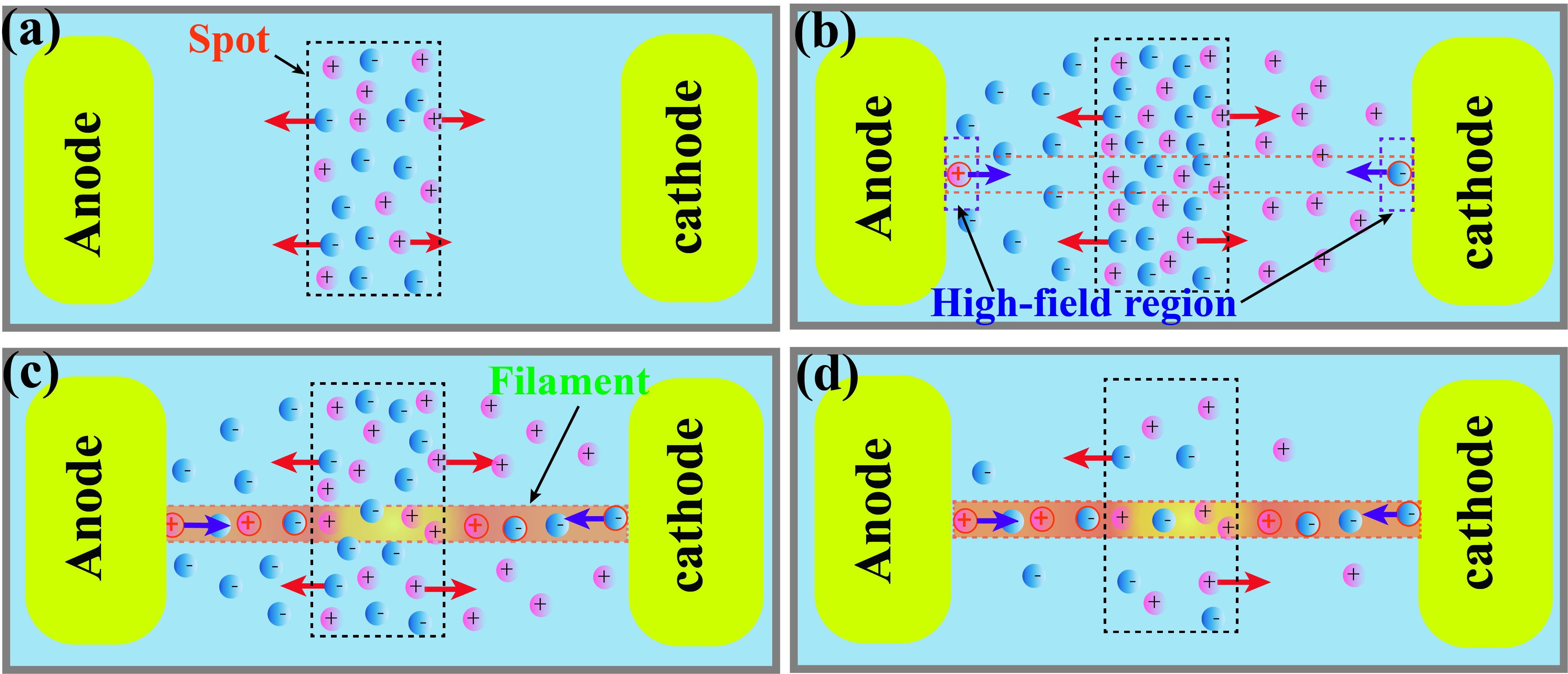
Fig. 5 The physical diagrams of carrier dynamic during the switching of the PCSS operating in the transition from the linear mode to the nonlinear mode. (a) Photogenerated carriers induce linear switching. (b) High-field static domains generate the ionization-produced carriers. (c) Linear switching and nonlinear switching within the filament co-exist in the switching transient. (d) The nonlinear switching continues after the laser has been extinguished. The blue dots and red dots without red circle represent the photogenerated electrons and holes, respectively. The blue dots and red dots with red circle represent the ionization-produced electrons and holes, respectively.
Download figure:
Standard imageAs the carriers are drifting toward the contacts to achieve the linear switching, the static high-field domains also gradually come into being near both the anode and cathode terminals, in which the peak field can reach over 200 kV/cm. The static domains play an essential role in injecting the ionization-produced carriers and generating the electron-hole plasma along a filamentary channel, as shown in figure 5(b). When the local electric field in the plasma region exceeds ~ 4 kV/cm, the classical Gunn-like domain instability starts to form the initial domains, then gradually converts the initial domains to the high-field, powerfully avalanche domains (> 250 kV/cm) due to the negative differential mobility (NDM) effect at the ultrahigh field. The formation and evolution of multiple powerfully avalanching domains inside the filamentary channel have been demonstrated to be the physical reason for the nonlinear switching of the avalanche GaAs PCSS [26‒28]. So, in figure 5(c), a co-existence state of the linear and nonlinear switching can be presented in the switching transient. Eventually, in figure 5(d), although the incident optical intensity is falling to weaken the linear switching, the nonlinear switching can still be continued until the applied bias voltage of the switch cannot sustain the voltage locking.
It is clear that the filamentary channel grows and develops on a fraction of the cross section of the total current channel. For the PCSS operating in the transitional state, its output waveforms will always integrate the characteristics of the linear and nonlinear modes, just as the double-peak phenomenon shown in figures 2 and 3. Correspondingly, the variation of these output waveforms can be attributed to the influence of the applied operating conditions on the nonlinear switching developing in the filamentary channel (active part) and the linear switching developing in the remaining channel (passive part) of the total current channel. Since the active and passive parts have a parallel relationship and the switching in the passive part always precedes that in the active part, the enhancement of linear switching can slow down the nonlinear switching. In contrast, the development of the nonlinear switching can restrain or cut off the linear switching. It is worth noting in our experiment, a thickened GaAs wafer with a thickness of 1 mm is adopted, and the extrinsic photoconductivity is employed by using the laser pulse with a wavelength of 1064 nm, together contributing to the total current channel with a larger cross section, which makes the transitional characteristic easier to be obtained.
It can be predicted that the increase of triggering energy mainly acts on the passive part to heighten the linear switching directly, although the triggering energy also accelerates the formation of avalanche domains in the active part to shorten the delay time of the nonlinear switching [26]. Different from the effect of the triggering energy, a higher bias voltage can induce the more drastic evolution of avalanche domains to enhance the avalanche multiplication [29, 30], thus strengthening the nonlinear switching in the active part, more significantly.
To verify the tight correlation between the output waveform and both the active and passive parts, under the condition that a spot approximately covering the whole switching area is used and the triggering energy is fixed at 100 μJ, the outputs are first tested at different bias voltages. As shown in figures 6(a)‒(c), influenced by the increasing bias voltages, the obvious uplift similar to that presented in figure 2 occurs on the falling edge of the output waveforms. In figure 6(c), the typical oscillation characteristic induced by the quenched-domain mode [23], has occurred on the tail of the output waveform. These evolution features mean that the increasing bias is boosting the switching in the active part toward the nonlinear mode. On the contrary, in figures 6(d)‒(f), influenced by the increasing triggering energy under Vb = 6.5 kV, the significant increase occurs on the parts induced by the linear switching, just like that shown in figure 3. The above results demonstrate the significant roles of the active and passive parts in determining the switching transient of GaAs PCSS.

Fig. 6 Output waveforms under (a)‒(c) different bias voltages and (d)‒(f) different triggering energies, at the spot size of 4.5×4.5 mm2. The gray areas approximately frame the parts dominating the increase of the output amplitude.
Download figure:
Standard imageBased on the above physic of two equivalent channels, the effect of spot size on the operation mode can be explained as follows. Under the fixed illuminating energy, the increase of the spot width will increase the cross section of the total current channel, decreasing the concentration of photogenerated carriers on the total channel. Considering that the cross section of the active part is always constrained within the region with an equivalent diameter of 50‒300 μm (corresponding to the diameter of the current filament) for sustaining the high current density for the nonlinear switching, this concentration variation will directly reduce the photogenerated carriers distributing on the active part to weaken the nonlinear switching, while making more photogenerated carriers injected into the passive part to strengthen the linear switching. As for the spot length, the extension of this size can be considered mainly along both the active and passive parts, which does not significantly change the cross section of the active part or passive part, but strengthens the formation and evolution of the domains on the active part. Due to the parallel relationship between the active and passive parts, the "winner takes all" principle [28] plays an important role during the switching process. The strengthened switching in one channel will thus inevitably suppress the switching developing in the other channel.
4.2. Domain evolution influenced by the spot size
The "two-channel" numerical model based on the theory of multiple avalanche domains has been demonstrated to be effective for interpreting the transitional switching transient of GaAs PCSS [20]. To further elucidate the inner domain dynamics influenced by the spot size, this predefined numerical model is introduced to simulate the GaAs PCSS. As shown in figure 7(a), the two equivalent channels of the GaAs PCSS are connected in parallel in the external circuit. The bias voltage is provided by a 0.14-nF capacitor Cs charged by a DC source via a 10-MΩ resistor Rs. At t = 50 ns, the 1064-nm laser pulse starts to trigger both parts, then the Cs discharges to the 50-Ω load. In the simulation, for higher computational efficiency, the coplanar structure of 30 μm×6 μm×6 μm is used to model the active part, and the bulk structure with a cross section of 30 μm×Ws and a length of 30 μm is used to model the passive part. The use of the scaling channels makes it difficult to directly compare the simulated outputs with the experimental outputs. However, the dimensions of the scaling structures are much larger than the domain dimension (submicron level to micron level), which can effectively support the comparative analysis of the domain evolutions under different spot sizes.

Fig. 7 (a) External circuit used in the simulation. (b) Typical currents through the active part (Ia), the passive part (Ip) and the load (IL) under Ls = 9 μm, Ws = 180 μm and ~ 30 kV/cm bias field. (c) Simulated IL and optical pulse under different Ls. (d) The Field distributions inside the active part at t = 50.7 ns and t = 51.4 ns. (e) The fields (Ecut) along the cutline of y = 0.01 μm of panel (d).
Download figure:
Standard imageKeeping the laser energy injecting the active and passive parts fixed, the typical currents through the load (IL), the active part (Ia) and the passive part (Ip) are calculated, and shown in figure 7(b). It is noted that the Ip has a waveform similar to the optical pulse and the Ia presents the characteristic of the typical ultrafast switching after a significant delay, thus we can observe a superimposed characteristic of the linear and nonlinear switching on the IL. As the Ls is extended from 9 μm to 18 μm, the significantly strengthened nonlinear part can be observed from the waveforms of IL shown in figure 7(c), presenting an evolution trend similar to that shown in figure 2, and allowing us to compare the domain evolutions under different spot lengths.
Figure 7(d) shows the spatiotemporal field distributions at t = 50.7 ns. It can be seen that the peak fields of the static domains are 147 kV/cm near the anode and 334 kV/cm near the cathode under Ls = 9 μm, but these values reach 230 kV/cm and 401 kV/cm, respectively, when Ls is extended to 18 μm. In addition, an initial domain forming on the boundary of the static domain near the anode, has already been observed under Ls = 18 μm. The initial domains will further evolve into the avalanche domains due to the NDM effect, as shown in the field distribution at 51.4 ns. These results demonstrate that a larger Ls can contribute to the earlier formation of initial domains by increasing the peak field of static domains, then speeding up the formation of avalanche domains to bring forward and heighten the nonlinear switching.
As for the reason why a wider Ls can peak the amplitude of static domains, it is attributed to the extended electric field shielding area [26, 29]. The shielding area is formed by the separation of the photogenerated electrons and holes, which introduces a built-in electric field with a vector direction opposed to that of the applied bias field, and appears with the appearance of the static domains. As shown in figure 7(e), a wider triggering region significantly leads to a larger electric field shielding area. Relative to the original size (the horizontal gap between the contacts), the shielding area is extended to ~ 43% under Ls = 9 μm and ~ 62% under Ls = 18 μm. The extended shielding area will compress significantly the spatial electric field of the active part, peaking the static domains.
The opposite trend of domain evolution can be expected in the active part when the switching process is influenced by the increasing spot width. In figure 8(a), a high bias field of ~ 67 kV/cm and a large spot length of Ls = 26 μm are used to induce the higher nonlinear outputs relative to the linear outputs, Thus, the effect of the increasing spot width on IL can be observed just from the switching stage of the output waveforms. Here, under the condition that the size of the active part and the illuminating total energy on both parts are fixed, the linear output under Ws = 1.8 mm presents a higher amplitude of 1.0 A than the amplitude of 0.5 A under Ws = 0.6 mm, or the amplitude of 0.8 A under Ws = 1.2 mm. Correspondingly, in figure 8(b), the apparent initial domain under Ws = 0.6 mm can be observed earlier than that under Ws = 1.8 mm, and the domain evolution under Ws = 0.6 mm is also faster than that under Ws = 1.2 mm. The larger width of the initial domain than that in figure 7(d) is attributed to the use of a larger spot length in the simulation. Because the domain evolution closely correlates with the carrier concentration in the current channel [29, 31], the slowing formation or evolution of domains also directly signifies the reduced photogenerated carrier concentration on the active part, when Ws is extended from 0.6 mm to 1.8 mm. Evidently, the above results demonstrate the explanation of the effect of the spot width on the operation mode.
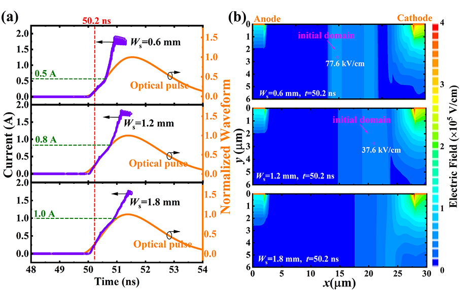
Fig. 8 (a) Simulated IL at the ultrafast-switching part and optical pulse under different Ws, where Ls = 26 μm and the bias field is ~ 67 kV/cm. (b) The field distributions inside the active part at t = 50.2 ns.
Download figure:
Standard imageBased on the characteristics of domain evolutions, the effect of spot size on the on-state performances of GaAs PCSS can be further discussed. Firstly, accelerating the formation and maturation of avalanche domains has been considered an effective strategy to improve the triggering efficiency of the PCSS [25]. That indicates, for the avalanche GaAs PCSS triggered by the fixed illuminating energy, the lower jitter and on-state resistance can be obtained by adopting a line-shaped spot along the filament. Secondly, in our study, the increasing peak field of static domains can induce more ionization-produced carriers, then reducing the demand for the photogenerated carriers before the ultrafast switching. So, for the actual avalanche GaAs PCSS, a reduced laser energy requirement can be achieved by increasing the spot length along the filament channel. Thirdly, considering that the increased spot width can broaden the total current channel to slow the domain evolution, we can conclude that a thicker (~ mm level) GaAs PCSS employing the extrinsic photoconductivity is more beneficial for strengthening the quasi-linear mode, to achieve the higher output power and longer device lifetime.
5. Conclusion
In summary, a coplanar GaAs PCSS with a 1-mm-thick wafer is adopted and triggered by a 1064-nm laser beam with the typical rectangular spot. The output waveforms integrating the characteristics of the linear and nonlinear modes are obtained, and the effect of the illuminating spot size on the output waveforms of GaAs PCSS is investigated experimentally. It has been found the variation of the spot size in length and width can act on the different parts of the output waveform, and then significantly boosts the PCSS toward different operation modes. On this basis, a two-channel numerical model composed of the active and passive parts is introduced, and the domain evolutions under different spot sizes are comparatively analyzed, which interprets well the relevant influencing mechanisms. It has been demonstrated that the increased spot length can peak the amplitude of static domains in the active part to enhance the development of nonlinear switching, while the extended spot width can change the distribution of photogenerated carriers on both parts to facilitate the linear switching and weaken the nonlinear switching. The corresponding research provides meaningful guidance for optimizing the illuminating spot to improve the on-state performances of GaAs PCSS.