
Abstract
Quantum dots (QDs) have sparked great interest due to their unique electronic, optical, and structural properties. In this review, we provide a critical analysis of the latest advances in the synthesis, properties, and applications of QDs. We discuss synthesis techniques, including colloidal and hydrothermal synthesis, and highlight how the underlying principles of these techniques affect the resulting properties of QDs. We then delve into the wide range of applications of QDs, from QDs based color conversion, light-emitting diodes and biomedicine to quantum-based cryptography and spintronics. Finally, we identify the current challenges and future prospects for quantum dot research. By reading this review, readers will gain a deeper understanding of the current state-of-the-art in QDs research and the potential for future development.
Export citation and abstract BibTeX RIS

Original content from this work may be used under the terms of the Creative Commons Attribution 4.0 licence. Any further distribution of this work must maintain attribution to the author(s) and the title of the work, journal citation and DOI.
Abbreviations
| QDs | Quantum dots |
| PL-QY | Photoluminescence quantum yield |
| PQDs | Perovskite QDs |
| LEDs | Light-emitting diodes |
| CVD | Chemical vapor deposition |
| PVD | Physical vapor deposition |
| TEM | Transmission electron microscopy |
| XRD | X-ray diffraction |
| HT | Hot injection |
| RT | Room temperature |
| UV | Ultra violet |
| QY | Quantum yield |
| CQDs | Carbon QDs |
| NCQDs | Nitrogen doped CQDs |
| SOP | Systems on panels |
| MIM | Metal insulator metal |
| RRAM | Resistive random access memory |
| ROS | Reactive oxygen species |
| QW | Quantum well |
| EQE | External quantum efficiency |
| UQDLs | Ultrafast quantum dot lasers |
| VCL | Visible light communication |
| ETL | Electron transport layer |
| HTL | Hole transport layer |
| ITO | Indium tin oxide |
| QKD | Quantum key distribution |
| FSO | Free space communication |
| QDCs | Quantum Dot Cryptosystems |
| MOF | Metal-Organic framework |
| IoT | Internet of Things |
| AI | Artificial intelligence |
| CA | Cysteamine |
| PeLEDs | Perovskite light emitting diodes |
| WLEDs | White light emitting diodes |
| CRI | Color rendering index |
| PSK | Polystyrene sulfonate potassium |
1. Introduction
QDs are tiny semiconductor nanoparticles [1, 2] just a few nanometers in size (ranging from a few nanometers to tens of nanometers) which possess one of the most important properties of quantum confinement [3]. Onyia et al [4] theoretically studied the effect of quantum confinement on QDs using particles in a box model. More generally, when a system has one or more dimensions small enough to affect its electronic density of states then the system is said to be confined. And accordingly, we have QDs in which electrons are confined in all directions which leads to larger oscillator strength for electronic transitions that can be used to make a wide range of electronic devices, including solar cells, LEDs, and transistors.
QDs have different properties than bulk materials like - size, as due to the small size of the QDs they have a high surface-to-volume ratio making them highly reactive (or active) whereas bulk materials are larger in size. QDs have discrete quantized energy levels in the density of states having (delta) like function shown in figure 1 [5] rather than a continuous range of energy levels like in bulk materials.
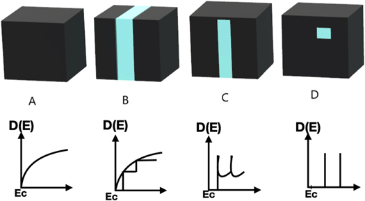
Figure 1. Schematic illustration of the changes in the density of states (DOS) where (A) Bulk material, (B) 2D, (C) 1D, (D) 0D.
Download figure:
Standard image High-resolution imageAt this scale, the electronic and optical properties of the material begin to deviate from those of the bulk material such as sharp absorption and emission spectra. In addition to this, QDs have an impressive ability to tune their band gap which can be effectively controlled by regulating the size of the QD. Also, several other methods of tuning the bandgap by alloying the core of the QDs were also demonstrated [6, 7]. This property is not found in bulk materials. Carefully controlling these properties makes QDs highly attractive for a wide range of applications in areas such as sensing [8], medicine i.e. light-based therapeutics and diagnosis [9, 10], biotechnology [11], optoelectronics, and materials science [12].
Different types of QDs have been used depending on types of applications and their unique properties. Early in the 1980s, the history of QDs may have been established when researchers first started looking into the characteristics of semiconductor particles small enough to display quantum confinement. Alexey Ekimov's research in 1981 is widely regarded as the first recorded experimental observation of quantum confinement in semiconductor nanocrystals, which are currently known as QDs. Using a chemical synthesis technique, Ekimov and his team produced cadmium selenide (CdSe) nanocrystals within a glass matrix, and they discovered that the nanocrystals' optical characteristics varied significantly from those of bulk CdSe, which classical physics could not explain [13]. In the following years, researchers began to explore other semiconductor materials for use in QDs, including cadmium telluride (CdTe), indium arsenide (InAs), and indium phosphide (InP). Each of these materials has unique properties because they have different band gaps that makes them well-suited for wide applications. For example, QDs based on the I-III-VI compositions, such as copper indium sulfide (CuInS2) and zinc sulfide (ZnS), are considered excellent alternatives to cadmium-based QDs for biomedical applications due to their lower toxicity. Moreover, in addition to being more biocompatible, Ag-In-S QDs [14] exhibited great potential for light absorption and emission. They also have a long photoluminescence (PL) lifetime and high quantum yields
CdSe is a good choice for use in optoelectronics [15] and bioimaging [16], while CdTe and InAs are used in solar cells and infrared detectors. These QDs can be grown from both organic and inorganic materials. QDs come in various structures, including the new Ternary I-III-VI type, which is a safer alternative to heavy metal-containing QDs. Copper indium sulfide (CIS) structures [17], with atoms arranged in a crystal lattice, are crucial for modern technologies. By altering the size of CIS QDs, their band gap can be adjusted, making them highly adaptable for use in solar cells [18] and LEDs [19], leading to more efficient devices with greater color variety. Additionally, CIS QDs are stable and easily synthesized, making them a promising material for applications such as biophotonics. Incorporating QDs into matrix structures creates nanocomposites with unique properties, improved stability, and enhanced mechanical properties. For instance, using CdZnTe QDs in a CaCO3 matrix [20] results in excellent photostability when compared to pure CdZnTe QDs. Additionally, the nanocomposite exhibits good processability, making it a promising material for various applications.
Perovskite QDs are a promising class of semiconductor nanoparticles that have gained significant attention in recent years due to their superior optical and electronic properties [21]. PQDs have high photoluminescence quantum yields, narrow emission bandwidths, and excellent color purity, making them a desirable alternative to conventional QDs. They also have the potential to be used in various optoelectronic devices, such as LEDs, solar cells. The development of PQDs has great potential to revolutionize the field of optoelectronics.
More recently, researchers have begun to investigate the use of other types of nanostructured materials, such as carbon nanotubes and graphene, as QDs. These materials have unique electronic characteristics and highly tunable Photoluminescence (PL) properties. This versatility makes them ideal for use in various fields, such as optoelectronics, sensing, and energy storage [8, 22]. Ongoing research is being conducted to find alternatives to heavy metal-containing and heavy metal-free emitters due to concerns such as toxicity and environmental impact. One such alternative is III-V QDs, particularly InP [23], which are being widely used in the development of next-generation displays.
Several growth methods were developed during the period to grow these nanoparticles suitable for different applications [24, 25]. However, there are different challenges or trade-offs faced by different applications because of the formation of these QDs for example inorganic QDs are toxic but show high stability against external parameters like temperature and humidity. On the other hand, organic QDs are non-toxic but can highly be affected by temperature, pressure, and humidity. Here, the cost and complexity of the synthesis process play a crucial role depending on the application requirements. Inorganic QDs [26] can be expensive to produce and may require high temperatures and pressures for synthesis while organic QDs are relatively inexpensive and abundant.
It's worth mentioning that researchers are working to overcome the toxicness of QDs [27] and trying to find new ways to use them in various applications. For example carbon QDs are showing great bio-compatibility to use in biosensing applications [8]. In this overview, we provide a brief examination of the structure, characteristics, fabrication, and various applications of QDs.
2. Structure of QDs
2.1. Quantum Vs bulk properties
A close arrangement of atoms or molecules is following the quantum rules referred to as QDs. In most cases, QDs consist of a core made of a semiconductor material and a shell made of a separate material that serves as a surface passivation layer. Different sizes and shapes of the core and shell are possible, and their qualities can be adjusted to fit particular applications. For instance, spherical QDs differ from rod- or disk-shaped QDs in their optical and electrical characteristics. The electrical and optical characteristics of QDs are determined by its core, while its stability and interactions are governed by the shell. The structure of the QDs are responsible for electrical and optical properties required for a specific application.
Quantum confinement, as previously established, is the characteristic that sets QDs apart from other bulk materials. Researchers have intensively studied the impacts of quantum confinement on semiconductor QDs [28–36]. When a QD follows the quantum confinement effect, the motion of excitons has been constrained to a quantized space leading to a quantum confinement giving QDs their distinctive optical and electrical properties. To achieve quantum confinement Bohr condition needs to be satisfied. This indicates the size of the nanoparticle must be smaller than the corresponding exciton Bohr radius [37].
One of the key differences between QDs and bulk materials is the size-dependent energy bandgap. In bulk materials, the bandgap is a property of the material itself and does not change with size. However, in QDs as shown in figure 2, the bandgap is inversely proportional to the size of the QD. The size of the QDs is important because it determines the strength of the quantum confinement effect. Smaller QDs exhibit stronger quantum confinement and have higher energy levels than larger QDs. Controlling the size of the QD during growth is a significant factor in the advancement and creation of new devices and their applications [36]. This size-dependent bandgap leads to a broad range of optical properties, including tunable absorption and emission spectra etc
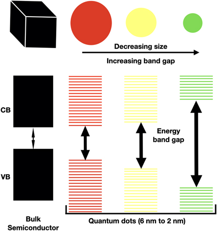
Figure 2. Schematic diagram showing energy band structures in bulk material and quantum nanostructure.
Download figure:
Standard image High-resolution imageFor example the bandgap of CsPbBr3 QDs increases from 2.3 to 2.5 eV with distinct blue shifts in the PL spectra when particle size decreases from 8.5 to 4.1 nm, according to Butkus et al's research [38]as shown in figure 3.
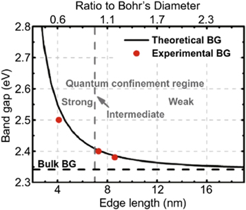
Figure 3. Experimental versus theoretical size-dependent bandgap energy of CsPbBr3. Reprinted with permission from [38]. Copyright (2017) American Chemical Society.
Download figure:
Standard image High-resolution image2.2. Optical properties of QDs
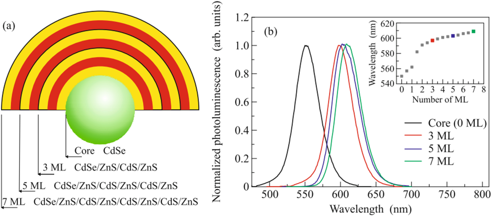
Due to their small size and the quantum confinement effect, QDs exhibit unique optical characteristics. Currently, there is a significant amount of research being conducted on core-multishell QDs. The structure consists of numerous shells made of various materials surrounding a central core made of a single material. By selecting different materials, the size and composition of the QDs can be altered, resulting in distinctive optical and electronic properties [39]. These different structures result in high photoluminescence quantum yields (PL-QY). The stability of the QDs is enhanced by the additional protection that the various layers offer the core. The core is typically made of a material with a direct bandgap, such as cadmium selenide (CdSe), while the shells are made of a different material, such as zinc sulfide (ZnS), that has a wider bandgap [40]. This multi shell design results in unique optical properties, such as broad and tunable photoluminescence and improved stability compared to traditional single-component QDs.
linkov et al proposed [41] a core-multishell QDs made of CdSe/ZnS/CdS/ZnS as shown in figure 4 as a substitute of a single shell. The multilayer shells have several advantages over single layered shells. For example, by adding different numbers of layers of shell increases, quantum yields have been achieved. These properties make core-multishell QDs useful in various applications such as LEDs, solar cells, and bio-imaging.

Figure 4. (a) Structure of a core-multishell QD (b) Photoluminescence spectra of QDs with different shell thickness. Reproduced from [41], with permission from Springer Nature.
Download figure:
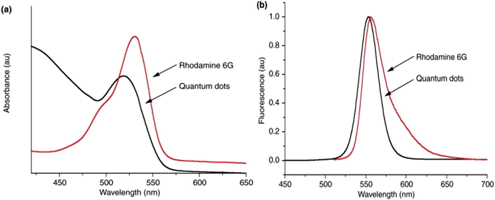
Standard image High-resolution imageThe optical properties of QDs are an important area of research, as they are related to the size, shape, composition, and surface chemistry of the dots. The optical properties of QDs can be tuned in many ways such that they can be taken as an advantage in wide applications. One such property shown in figure 5 is their broad and continuous excitation profile, which means they can be effectively excited at any wavelength below 530 nm. This is in contrast to organic dyes like rhodamine 6 G [42], which have a limited excitation range and a wide emission spectrum. Additionally, QDs have almost symmetrical and narrower emission spectra compared to organic dyes. These properties make QDs more versatile and efficient in a wide range of applications.
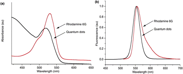
Figure 5. Excitation (a) and emission (b) profiles of rhodamine 6 G and CdSe QDs. Reprinted from [42], Copyright (2002), with permission from Elsevier.
Download figure:
Standard image High-resolution imageOther QDs such as inorganic perovskite QDs (PQDs) are a type of nanomaterials that have gained attention in recent years due to their unique optical properties. They have a high quantum yield which is the fraction of absorbed photons that are emitted as photoluminescence. This property makes PQDs efficient light emitters and is important for applications where high light output is required. Strong and focused PL light emissions are seen from inorganic perovskite QDs. Inorganic perovskite QDs (PQDs) can exhibit a photoluminescence quantum yield (PLQY) greater than 99% without the need for surface passivation through the use of wide-bandgap epitaxial shells, unlike conventional semiconductor QDs such as CdSe, CdS, or PbS [43].
To overcome the limitations of the structural properties of QDs various compositional types of QDs including doped QDs are utilized. These QDs contain impurities or dopants, typically metal or non-metal elements, incorporated into their core or shell structure, which introduce new electronic states into the QD, thereby modifying its properties such as bandgap, charge carrier dynamics, and emission wavelength. The dopants can be carefully controlled to tailor the QD's properties for specific applications. Doped QDs have been found to enhance the performance of optoelectronic devices such as light-emitting diodes by improving their efficiency and stability. Another class of semiconductor QDs that is alloyed semiconductor QDs have emerged as a significant area of research due to their unique optoelectronic properties. These QDs consist of a single crystalline structure made up of two or more different materials with varying sizes [44]. The composition and size of these constituent materials are controlled to modify the properties of the resulting QD for specific applications. For example, To adjust the emission of CdSe QDs, alloying them with ZnSe [45] is a common approach as it is challenging to control their emission solely through the quantum confinement effect. This method enables the tuning of the bandgap energy and allows for more precise control over the emission wavelength of the QDs. Alloyed QDs exhibit improved luminescence efficiency, thermal and photo stability, and reduced sensitivity to external factors like moisture and temperature.
2.3. Surface passivation
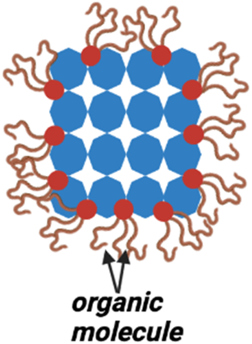
The surface of the QD can significantly affect the electrical and optical properties of QDs. Hence surface passivation is necessary for QDs. Device efficiency and stability can suffer due to surface-induced defects and trap states that impact carrier recombination. The size and shape of QDs can also be influenced by the surface. In order to address these problems, surface passivation is used to 'heal' the surface of the dot. The development of different ligand structures which covalently bonded with the QDs in turn act as a protective coating or capping layer. This procedure increases the stability and effectiveness of the device. It further lowers the density of defects and trap states and can help to maintain the size and shape of QDs. Overall, the passivating layer must be able to protect the surface from environmental degradation. Numerous studies have investigated how surface passivation affects a material's optical and electrical characteristics. Improving luminescence qualities by preventing non-radiative recombination and minimizing defect states. Although ligands help ensure that QDs are in a stable phase, having too many capping ligands on the surface of the QDs potentially makes charge transport difficult which impacts the optoelectronic properties of Light-emitting Diodes (LEDs) [46]. The choice of passivating layer is important to obtain high performance and stability of the QDs. High electron mobility, a low surface recombination rate, and strong chemical stability are all desirable qualities in a passivating material. There are several different methods that have been proposed for the surface passivation of QDs, including the use of organic ligands that act as a capping agent shown in figure 6 [47–49], inorganic coatings, and self-assembled monolayers.
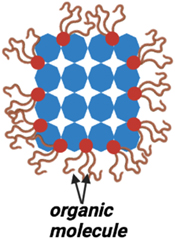
Figure 6. Schematic illustration of organic capped Quantum dot.
Download figure:
Standard image High-resolution imageJung et al reported the creation of high-quality QDs using environmental friendly electrically active metal chalcogenide complex ligands (Sn2S6 4−, Sn2Se6 4−, and In2Se4 2−). This ligand helps to stabilize the QDs in polar solvents such as formic acid, dimethylformamide (DMF), N-methylformamide, and dimethyl sulfoxide (DMSO). This method showed improvement in the stability and charge transport in devices [50].
3. Synthesis and characterization of QDs
Synthesis and characterization of QDs refer to the process of creating and studying the properties of QDs. Synthesis involves the methods used to create QDs, such as colloidal synthesis, chemical vapor deposition (CVD), and physical vapor deposition (PVD). Characterization involves studying the properties of the QDs, such as size, shape, composition, and optical properties. This can be done using techniques such as transmission electron microscopy (TEM), x-ray diffraction (XRD), and spectroscopy (such as absorption, photoluminescence, and Raman). The aim is to understand the relationship between the synthesis conditions and the resulting QD properties. Finally, it has been discussed the optimization of synthesis conditions to produce high-quality QDs with desired properties for different applications.
3.1. Colloidal synthesis
Colloidal synthesis is a widely used method for producing QDs, and the high-temperature version is particularly effective. Murray, Norris, and Bawendi first proposed this chemical technique in 1993 to produce QDs [49]. The process involves dissolving metal ions or organometallic compounds, known as precursors, in a solvent, and then subjecting them to various chemical or physical treatments to create the desired QDs. The primary advantage of this synthesis method is its ability to produce QDs of varying sizes with great ease, making it highly tunable [51, 52].
One of the popular techniques of colloidal synthesis is the 'Hot Injection Method'. In this a precursor solution containing the appropriate elements is quickly injected into a hot, high-temperature reaction mixture. As a result, the precursors react quickly to generate QDs, which quickly cool and solidify. By adjusting the type, the concentration of the precursor, reaction time, and temperature during synthesis, the size and composition of colloidal QDs can be controlled [53]. This approach allows for the efficient and rapid synthesis of high-quality QDs of homogeneous size distribution (shown in figure 7) in large quantities.
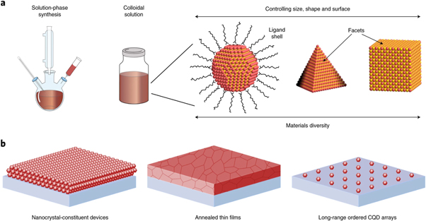
Figure 7. Colloidal QDs, The solution-processed synthesis resulting in colloidal nanocrystal inks, self-assembly of QDs with highly monodispersed size and shape leads to long-range ordered superlattices. Reproduced from [54], with permission from Springer Nature.
Download figure:
Standard image High-resolution imageThe colloidal QDs is particularly useful for the synthesis of inorganic QDs, such as CdSe or CdS and halide perovskites [55]. Irshad Ahmed et al as shown in figure 8 [56]demonstrated the synthesis of CdSe QD in the 'Hot Injection Method' versus 'Room temperature method'. It was noted that the smallest QD created using the HI-method had a size of 2.5 nm. Only QDs with a 3.3 nm size could be manufactured using the RT approach. The effect of synthesis protocol on the fluorescence property was also studied in figure 9 and compared with the RT method. The HI-QDs demonstrated high photochemical stability, indicating their potential for use in the development of optoelectronic devices. This synthesis method offers several advantages over other methods, including precise control on the size and shape of the QDs, high purity, and low defect density. The process is relatively straightforward to scale up, and it can be used to produce a broad range of different QD types. As a result, this method has been extensively used in recent years to produce high-quality QDs for various applications.
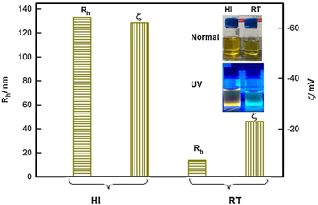
Figure 8. Under bright light and ultraviolet (UV) illumination, the two procedures for CdSe quantum dot synthesis. Reprinted from [56], Copyright (2016), with permission from Elsevier.
Download figure:
Standard image High-resolution image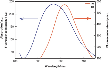
Figure 9. Fluorescence spectra of the Quantum dot samples obtained from Hot Injection (HI) and Room Temperature (RT) synthesis. Reprinted from [56], Copyright (2016), with permission from Elsevier.
Download figure:
Standard image High-resolution imageSignificant amount of data has been produced on QDs by experimentalists and theorists. Machine learning methods used to analyze this data, identify patterns, and accurately make the predictions. For example, Krishnadasan et al developed an autonomous black-box system to control the synthesis of CdSe QDs in a microfluidic reactor [57, 58]. By utilizing a global search algorithm SNOBFIT, they discovered the optimal injection rate and reaction temperature, which increased the emission intensity at a specific wavelength [59].
New precursors, capping agents, and synthetic techniques have recently been developed in colloidal synthesis, allowing exact control over the QDs' size, shape, and makeup. For instance, using PEG or DHLA (dithiol-PEG-dithiol) as ligands for capping can result in creation of extremely monodisperse QDs with precise size and shape.
Aqueous-based synthesis is one of the cost-effective and environmentally friendly methods to synthesize stable colloidal QDs. This method involves a solution-based chemical reaction using precursor solutions and a base to trigger nucleation and growth of QDs in a colloidal solution, without the use of toxic solvents or high temperatures. core–shell QDs can be easily grown using this technique to produce highly luminescent QDs. Reza Sahraei et al [60] have developed a growth-doping strategy for the one-pot synthesis of water-soluble dual-doped Ag,Ni:ZnCdS/ZnS core/shell QDs, which is a novel approach.
3.2. Hydrothermal synthesis
The hydrothermal method is a simple and low-cost method for the preparation of QDs with well control on size and shape. In this method, a precursor solution containing metal ions and ligands is placed in a sealed container and heated under high pressure in a water bath. As the temperature and pressure increase, the solution becomes supersaturated, hence nucleation of the QDs occurs. The size and shape of the QDs can be controlled by varying the reaction parameters such as temperature, pressure, and reaction time. One of the advantages of hydrothermal synthesis is that it allows the synthesis of QDs at relatively low temperatures compared to other methods such as high-temperature furnaces or molecular beam epitaxy. Hydrothermal synthesis is a method for synthesizing QDs in which a precursor solution is heated in a sealed vessel (typically a high-pressure autoclave) at high temperatures and pressures.
Zhu et al presented a straightforward hydrothermal method for producing uniform, mono dispersed SnO2 QDs with a narrow diameter range in their study (2.3 to 3.1 nm). The key to the hydrothermal technique described here is to use the hydrazine hydrate, or N2H4H2O, which serves as both an alkali and a ligand to coordinate with the Sn ions and create a complex cluster [61].
The hydrothermal method offers an easy way to create high-quality cysteamine-stabilized CdTe QDs, whose quantum yield (QY) can reach 19.7% under ideal conditions reported by Wei-haiYang et al [62]. The growth rate is faster than the aqueous method in which the CdTe QDs were grown at 220 °C for 20 min. During this time the absorbance peak changed from 490 nm to 640 nm shown in figure 10 and the mean particle sizes changed from 2 nm to 4 nm.
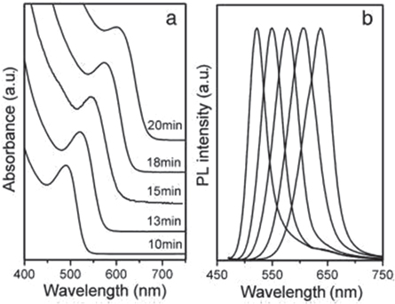
Figure 10. Change in the absorption and photoluminescence spectra over time for CdTe QDs covered with a CA cap. Reprinted from [62], Copyright (2008), with permission from Elsevier.
Download figure:
Standard image High-resolution imageHydrothermal synthesis allows for the synthesis of QDs such as carbon QDs (CQDs) doped in nitrogen forming NCQDs. This has successfully proven to be a good imaging agent that can be beneficial for certain applications such as bioimaging [63]. Because of its straightforward operating conditions such as low energy requirement, and inexpensive apparatus, hydrothermal synthesis is thought to be the most accessible approach. The basic schematic illustration of this synthesis approach is given in figure 11.
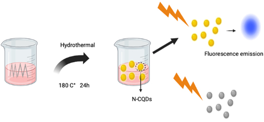
Figure 11. Schematic illustration of the synthesis of nitrogen-doped carbon QDs (N-CQDs) by a hydrothermal treatment approach.
Download figure:
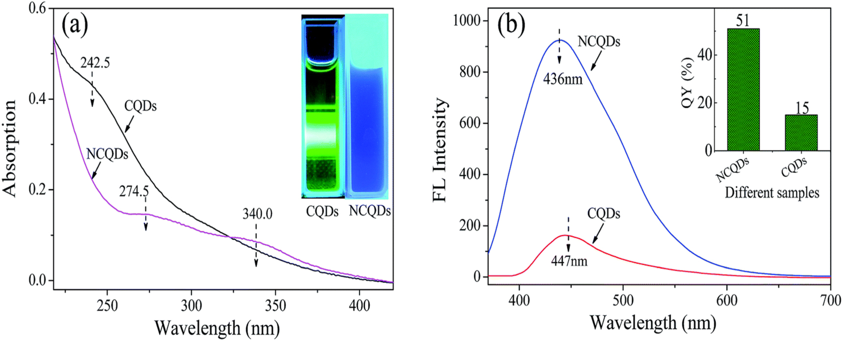
Standard image High-resolution imageCQDs created using this synthesis technique, however, frequently have a poor fluorescence quantum yield (QY) of less than 10% [64]. Doping with nitrogen has been demonstrated to be a successful method of enhancing these qualities in order to counteract this effect [65]. The numerous benefits of CQDs can be retained by nitrogen-doped CQDs (N-CQDs), but they can also overcome this drawback. In addition, the carbon sources utilized to create N-CQDs have a significant impact on their QY and optical properties. It can be observed from figure 12 that the fluorescence emission intensity of N-CQDs is stronger than that of CQDs solutions with the same concentration. Peng wu et al [66] synthesized the N-CQDs by the hydrothermal method and it showed that these N-CQDs have been demonstrated to be effective as a fluorescent probe for detecting Fe3+ ions in highly acidic environments. This is due to their superior fluorescence emission properties that result in good selectivity and sensitivity to Fe3+ ions.

Figure 12. (a) UV–vis absorption spectra of NCQDs and CQDs irradiated at 360 nm. (b) Fluorescence emission spectra of NCQDs and CQDs excited at 360 nm. Reproduced from [66] with permission from the Royal Society of Chemistry.
Download figure:
Standard image High-resolution imageHydrothermal synthesis also has few limitations. The high-pressure and temperature conditions required can be challenging to control, which can make it difficult to obtain highly uniform and monodisperse QDs [67]. Hydrothermal process is relatively cost-effective, as it only requires a few precursor materials, an autoclave, and an oven, while reflux methods often require a Schlenk line and an oxygen-free medium, with the need for multiple precursor injections during synthesis.
Some recent advances in the hydrothermal synthesis of QDs include the development of new precursors and surfactants that can be used to improve the size and shape control of the QDs. Additionally, researchers have been exploring the use of alternative solvents such as ionic liquids and supercritical fluids [68], which can offer improved solubility of precursors and better control over the reaction conditions and can result in high quality and uniform QDs with a narrow size distribution.
3.3. Biomimetic synthesis
Biomimetic synthesis of QDs refers to a process of synthesizing QDs using biological materials. In this process, the growth and self-assembly of QDs are mimicked based on the mechanisms and principles found in biological systems. The use of biomimetic techniques in the growth of QDs has several advantages over traditional synthetic methods. High temperatures, harsh chemicals, and high pressures are frequently needed in these conventional synthetic processes in order to grow the QDs. Large size and uneven distribution, as well as flaws and impurities may occur under these circumstances. This leads to an impact on the optical and electrical capabilities of QDs. However, the development of 'green' biomimetic mineralization technology makes the production of (II-VI, IV-VI, and I-VI) QDs simpler. The use of enzymes, proteins, or microorganisms as catalysts can help to reduce the use of harsh chemicals and high temperatures, making the synthesis process more environmentally friendly and biocompatible [69]. Additionally, the use of Biomolecules such as proteins, enzymes, and DNA are used to stabilize the QDs and control their size, shape, and surface properties. These biomolecules help to reduce the formation of defects and prevent the aggregation of QDs, ensuring that they remain well-dispersed and stable. The synthesis process typically involves the introduction of the precursors for the QD formation into a reaction medium containing the stabilizing biomolecules and the biotemplate. The reaction medium is then subjected to specific conditions, such as temperature, pH, and time, to allow the QDs to grow. The resulting QDs are then separated from the reaction medium and purified, if necessary. Overall, biomimetic synthesis is an important approach for producing high-quality QDs for various applications in optoelectronics, energy, biology, and medicine.
Li et al [70] discovered a straightforward, one-pot, environmentally friendly method to make CdSe QDs using lysozyme (Lyz) and bovine serum albumin (BSA) as the respective biotemplates. Bacterial cells were then marked with the BSA-functionalized CdSe QDs that had been produced. And it was determined that lysozyme's biological activity persisted after CdSe was formed, which is essential for creating fluorescent nanoprobes with biological function.
A work done by Arriaza et al [71] where they demonstrated a biomimetic approach shown in figure 13 for synthesizing CIS (CuInS2) QDs, which proved to be a green chemistry approach that retains some biological characteristics in the chemical process. CIS nanoparticles are the top choice for numerous technical applications, including solar cells and biomedicine [72].
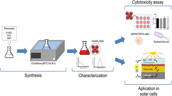
Figure 13. Overview of synthesis and characterization of CIS QDs. Reprinted from [71], Copyright (2021), with permission from Elsevier.
Download figure:
Standard image High-resolution image3.4. Other synthesis process
Rapid and easy synthesis techniques are crucial for scientists to conduct more precise experiments within a short period while minimizing heat release into the environment. Microwave-assisted synthesis [73] provides a rapid and easy alternative energy source that is widely used due to its control over the heating of materials. This method has proven to be effective for QD preparation, with several studies confirming its feasibility and potential. QD precursors are dissolved in a solvent and irradiated with microwaves in a reactor, resulting in the formation of QDs with a narrow size distribution and high crystallinity [74]. Microwave-assisted synthesis has many advantages over traditional synthesis methods [75, 76], including shorter reaction times, reduced energy usage, and better product yields. It also provides accurate control over the size and shape of the QDs, which is crucial for many applications.
4. State-of-the-art applications of QDs
Electronics, chemistry, physics, and biological sciences are just a few of the domains shown in figure 14 where QDs can be used because of their unique properties [77]. The configurable characteristics of QDs, including their size, shape, material, and ligand selection, are what cause them to exhibit this variation. The duration, temperature, and synthesis process [78] can all be accurately adjusted to control these various characteristics. This section of the article will examine QD applications that have drawn considerable interest across a range of industries.
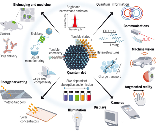
Figure 14. Application of QDs. From [88]. Reprinted with permission from AAAS.
Download figure:
Standard image High-resolution image4.1. QDs in memories
QDs have a high electron mobility and a large bandgap. This makes them useful for high-performance electronic devices such as neuromorphic computing hardware devices [79–81], floating gate capacitive memory structures etc Also, semiconductor QDs have become a highly desirable candidate for photonic applications because of the compatibility with CMOS-based solution processing methods. These devices have excellent optical absorption coefficient, structural stability, and ability to be produced in high quantities with low cost, large area coverage. Jeong et al [82] created a quick photo-induced recovery of CdSe QD floating gates in low-intensity light shown in figure 16.
Mondal et al conducted research that showed two-terminal, all-inorganic, spin-coated Al/ALPO/CdTe: ALPO(4:1) ALPO/Active Layer-Si capacitive memory systems that use CdTe-NP for charge storage and ALPO as the dielectric. Systems on panels (SOP)can be employed with these constructions [83]. The maximum memory window can be obtained from the width of the hysteresis shown in figure 15.
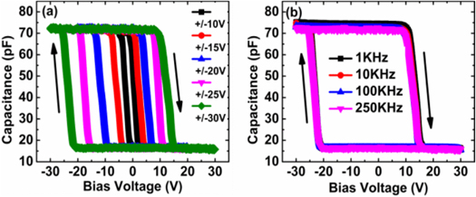
Figure 15. (a) C-V curves at 250 KHz with different DC bias sweep ranges; (b) CV curves at different frequencies. © 2016 IEEE. Reprinted, with permission, from [83].
Download figure:
Standard image High-resolution imageInorganic perovskite QDs have been explored as a material for resistive random access memory (RRAM) memory devices due to their unique electrical and optical properties. RRAM has great promise for data storage, logic operation, and neuromorphic devices. It offers the benefits of great scalability, simple (MIM) metal-insulator-metal structure, long data retention, inexpensive manufacture, and nanosecond speed, offering a lot of promise for improving memory. Incorporating QDs also makes it possible for memory cells to be smaller, which is crucial for the creation of high-density memory devices. The RRAM devices are made by incorporating these QDs into the active layer of the device [84]. In RRAM, the resistance of the memory cell can be switched between high and low resistance states by the application of an electric field. RRAM devices have higher device performance, better memory retention, and less leakage current because of usage of inorganic perovskite QDs.
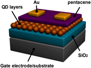
Figure 16. Schematic illustration of OFET incorporating CdSe QDs. Reprinted with permission from [82]. Copyright (2018) American Chemical Society.
Download figure:
Standard image High-resolution imageAnother type of memory devices which are in active research is QDs based memristor. The idea of employing QDs as the active element in memristor devices has gained popularity in recent years with the advantages of providing higher tunaility, ability to integrate with electronic devices and low power consumption. Memristors are a type of non-volatile memory device that can store information based on the resistance of a material. A ZnO/CsPbBr3 QDs-based memristor with a high ON/OFF ratio (>105) and a low working voltage (1 V) was demonstrated by Wu et al [85]. The development of memristors using several QD types, including organic QDs, metal-oxide QDs, and inorganic perovskite QDs, has advanced and to enhance the device stability [86, 87]. The development of QD-based memristors still faces some difficulties and constraints, such as the requirement for reliable and effective fabrication processes, development of environmentally friendly lead inorganic perovskites and the difficulties in regulating the size and composition of the QDs.
4.2. Biomedical applications
QD-based nanomaterials have been proven a competition to non-biomedical applications such as displays and other applications. However, one needs to make an appropriate choice when considering this application. There are several harmful effects and compatibility issues with biological systems. The use of toxic materials, high cost, and much greater size compared to organic dyes are some of the drawbacks of QDs-based detection techniques. The properties of QDs may be impacted by their toxicity. Heavy metals like cadmium, lead, or zinc, which can be hazardous to both the human body and the environment. These heavy metals can be released and be harmful if QDs are not properly encapsulated or if they are broken down. If the QDs are degraded or their chemical composition is altered due to toxicity, their optical properties such as their absorption and emission spectra, quantum yield, and photoluminescence lifetime may change. The type of solvent employed in the synthesis, the nanoparticle coating, and particularly the metals required to grow the QDs have been all linked to the toxicity [88]. These restrictions may impede the use of QD-based bioassays to replace well-established dye-based testing. For instance, a solid tumor may get only 0.7% of the injected nanoparticle dose, which is unsatisfactory [89]. As a result, the use of such kinds of QDs in therapeutics and diagnosis has been limited. In addition, numerous factors contribute to the limited use of nanomaterials in biological applications. One of them could be pointed out as a lack of in-depth knowledge of nano-bio interactions [90]. The gaining of knowledge on the complexity of biological systems and translating it to nano parameters is an important factor. Therefore, it is important to accurately adjust these characteristics for successful implementation of nanomaterials, particularly QDs in biological systems. The processing of QDs of this kind is demonstrated through flowchart as shown in figure 17.
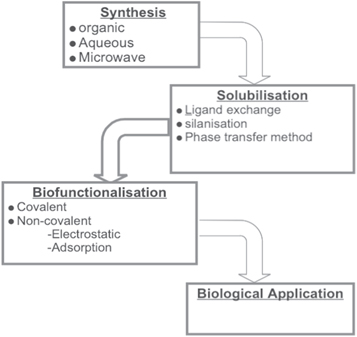
Figure 17. Flow of processing QDs for Biomedical applications.
Download figure:
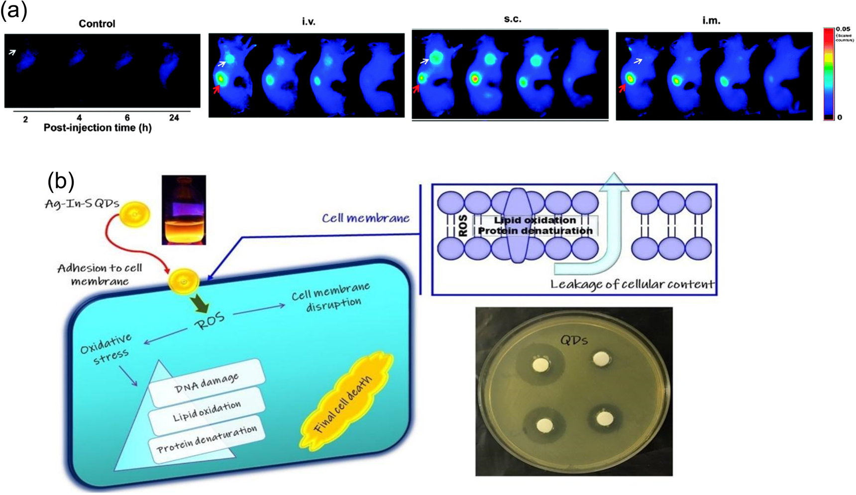
Standard image High-resolution imageQDs have the potential applications in the biological fields starting from imaging, biosensing, and therapeutics [91]. For cell staining, animal imaging, and tumor biology research- multicolor imaging with QDs is often performed [92]. To achieve these objectives, fluorescence-based detection methods are suitable [93]. For the fluorescence detection method, the characteristics of QDs such as fluorescence life-time, photochemical stability, fluorescence quantum yield, and emission anisotropy, gives high resolution (nanoscale) and substantial sensitivity to detect down to the single-molecule level [94]. Nucleic acids and proteins can be specifically detected using QD-labeled DNA probes [95, 96]and antibody molecules [97]. QDs are being widely employed in biotechnology and the medical industry as the substitutes for organic and fluorescent dyes. They are also being used for creating the next generation of biological labels, which helps to overcome the drawbacks of traditional organic dyes and other fluorophores [94]. CQDs for example are also particularly alluring in the field of nanomedicine because they do not exhibit any outward indicators of toxicity in animals and can be employed for in vivo studies. One such study was conducted by Xinglu et al [98] shown in figure 18(a) where CQDs were orally given to mice, and they were then examined four weeks later. It was determined that their internal organs and processes are rarely impacted. Antibacterial activity is one of the most attractive applications of QDs. Due to QDs capacity to produce reactive oxygen species (ROS) when exposed to light, which can result in oxidative damage to bacterial cells shown in figure 18(b). QDs are a promising method for preventing bacterial infections because this can result in cell death or growth inhibition. The majority of earlier studies on the antibacterial effects of QDs used cadmium-based (Cd) QDs, which are hazardous to biological systems and cause time-dependent cell death by actually releasing free Cd2+ ions, which are extremely toxic, even when Cd species was covered by a non-toxic shell [100]. QDs have additional benefits over conventional antibacterial agents in addition to their antibacterial effectiveness. They target bacterial cells more effectively due to their large surface area to volume ratio. They are more stable and have a longer shelf life than conventional antibiotics, making them simpler to store and transport. Nanoparticles like ZnO have been receiving a lot of attention due to the high exciton binding energy (60 meV) and wide band gap energy,(3.37 eV). Moreover, under normal illumination conditions, it also has a variety of antibacterial effects on different microbes, and activation by UV photoirradiation increases its antibacterial activity [101].

Figure 18. (a) Images of SCC-7 tumor-bearing mice captured using near-infrared (NIR) fluorescence at different time points, including 2, 4, 6, and 24 h after injection. The study includes a control group without injection, as well as groups injected intravenously (IV), subcutaneously (SC), and intramuscularly (IM). The images indicate the presence of tumors with a white arrow and kidneys with a red arrow. Reprinted with permission from [98]. Copyright (2013) American Chemical Society. (b) Antibacterial activity of QDs: Formation of ROS species. Reprinted from [99], Copyright (2019), with permission from Elsevier.
Download figure:
Standard image High-resolution image4.3. Optoelectronic devices
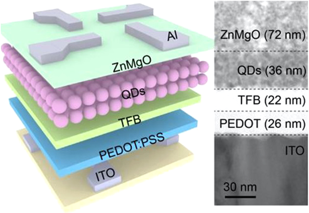
QD light-emitting diodes (QD-LEDs) is a type of LED that utilizes QDs as the active material in the emissive layer. The key advantage of QD-LEDs over traditional LEDs is that the QDs can be engineered to emit light at specific wavelengths, which allows for more precise color tuning and improved efficiency. Moreover, QLEDs used QDs to emit light, which results in a wider color gamut compared to traditional LEDs and produces a brighter and more intense light. It makes them ideal for large displays and high-resolution applications. For this reason, QD-LEDs are used in the display technology, which has high display performance and low manufacturing costs. InP-based QDs are emerging as a favorable and environmentally friendly option for light emission in display applications. Haiyang Li et al [102] have developed an easy and efficient method to create InP/ZnSe/ZnS core/shell/shell QDs shown in figure 19 with a PL-QY close to 100%. These QDs have a narrower emission line width and greater thermal stability compared to QDs produced using hydrofluoric acid.

Figure 19. Scheme of the QLEDs and cross-sectional TEM image of the QLED. Reprinted with permission from [102]. Copyright (2022) American Chemical Society.
Download figure:
Standard image High-resolution imageAdvancements in epitaxial processes over the past 30 years have led to significant breakthroughs in the field of semiconductor optoelectronic devices. The transparency current is decreased by quantum confinement as a result of rapid charge carrier filling at the energy of the working transition. The population inversion with lesser injected carriers causes an optical gain that depends on the injection current. The large overlap between the electron and hole wave functions because of the high degree of confinement increases the oscillator strength of the transitions [103]. The gain is expected to increase with a smaller physical size of QDs [104]. Additionally, in comparison to quantum well (QW) devices. The essential parameters like the chirp-factor, and linewidth enhancement factors which act as a performance metric in different lasers. In case of QD lasers these factors are substantially smaller [105, 106]. This is because QDs have more symmetric gain function compared to its QW and bulk equivalents. QD lasers have excellent temperature stability which allows them to operate at higher temperatures with less power consumption. It can be further optimized followed by a proper device design. Introducing the p-type doping in QD lasers has significantly improved thermal stability. The need for precise control over the shape and size of the QD reduces by doping with p-type materials [107, 108]. A 65% decrease in the threshold (of transparency current) at 300 K was achieved due to the incorporation of a p-type dopant, which also showed a minor increase in non-radiative recombination and increased modal gain as a function of the transparency point [105]. Another interesting method to increase the gain is by applying strain. Generally, strain is incorporated by the pseudomorphic growth of semiconductor layers [109]. Slightly lattice-mismatched semiconductor layers are grown over one another to realize strain. Theoretically, the maximum strain that could be realized for common semiconductors like Si, GaAs, etc is around 4%. Active research is going on to explore the impact of strain on optoelectronic properties of 2D materials and in QDs [110].
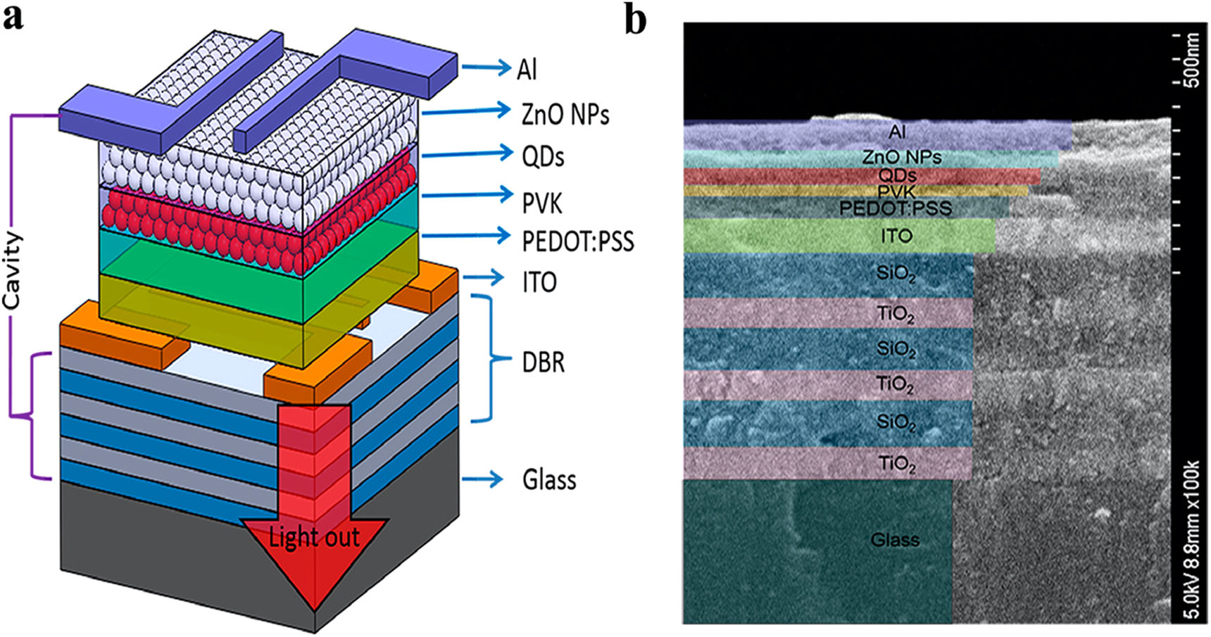
The highly effective auger recombination process is non-radiative in nature and results in the emission of phonons. The auger recombination process results in the loss of energy from the system and reduces the efficiency of the laser or LEDs (this phenomenon is also referred to as Droop). This happens at high driving currents which present a significant challenge in the realization of lasing [111]. As shown in figure 20, external quantum efficiency (EQE) versus the current density of QD-LEDs with different types of QDs is given. EQE is roughly constant up to the current density of (J = 10 mA cm2) regardless of the kind of QDs used in the LED, and thereafter it steadily drops at larger currents [112]. The high carrier density and small dot size can cause significant Auger recombination, which can lower the threshold current density and laser efficiency. A variety of techniques has been employed to counteract this effect, including improving the size and composition of the dots, lowering the density of defects, and employing several QDs of various sizes. The use of better optical feedback structures, and tailored optical waveguides are suggested to improve lasing. By incorporating microcavity structures in the device Wang et al [113] proposed a QLED with high EQE shown in figure 21.
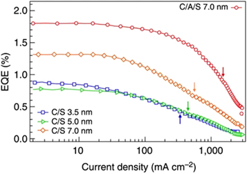
Figure 20. EQE versus current density of QD-LEDs with different types of QDs. Reproduced with permission from [112]. CC BY-NC 4.0.
Download figure:
Standard image High-resolution image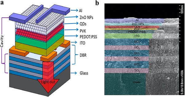
Figure 21. (a) Schematic device structure of QLED. (b) Cross-section SEM image of the device. Reprinted with permission from [113]. Copyright (2020) American Chemical Society.
Download figure:
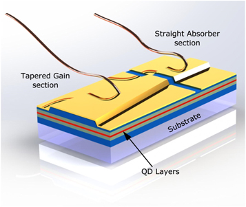
Standard image High-resolution imageRecent advances show that QDs are even used for ultrafast lasers as the QDs offer broad optical gain bandwidth. Ultrafast QD lasers (UQDLs) like mode-locked QD lasers shown in figure 22. This type of laser utilizes QDs (QDs) as the active medium. They are characterized by their ultrafast temporal response, which means they can generate extremely short light pulses of the order of picoseconds or femtoseconds. The fabrication of UQDLs is challenging and requires advanced techniques such as colloidal synthesis, vapor-phase growth, and molecular beam epitaxy [115]. The main advantage of mode locked QDLs is their ability to generate ultrafast pulses of light, which makes them useful in a wide range of applications such as spectroscopy, sensing, and telecommunications.
Download figure:
Standard image High-resolution imageOne of the important characteristics of QDs LEDs (QLEDs) is shelf stability. The shelf stability of QD-LEDs is a critical aspect for their commercialization. It indicates the LEDs' capacity to keep up their effectiveness and quality during the course of storage. For QD-based LEDs, shelf stability is influenced by many factors like the type of materials used in the active layer, size, shape, composition and method of encapsulation. Shelf stability can be increased by encapsulating the QDs [116] within a protective layer such as polymer coating or glass as one of the primary reasons for the degradation of QDs is their exposure to air and moisture. Encapsulation can prevent exposure to air and moisture and improve the shelf stability. It is challenging to achieve shelf stability in QLEDs due to the material degradation, surface oxidation, and fusion. Ye et al [117] induced a bilayer structure shown in figure 23 to increase the shelf stability. The performance of a device built on s-ZnO changes the function of shelf-storage duration. EQEmax rises from 10.3% (at fresh) to 14.9% (at day 7) shown in figure 24 by reducing the threshold voltage (Vth) from 1.8 V to 1.7 V.
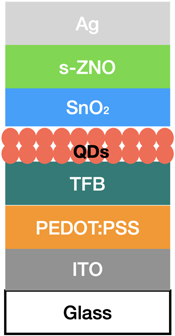
Figure 23. QLED with a SnO2-ZnO bilayer ETL device structure.
Download figure:
Standard image High-resolution image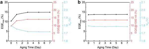
Figure 24. EQEmax, Vth, of QLEDs (a) with s-ZnO or (b) SnO2/s-ZnO as ETL. Reproduced from [117]. CC BY 4.0.
Download figure:
Standard image High-resolution imageIt is also possible to achieve shelf-stability during the process of fabrication y by preventing the deactivation of the light-emitting properties of the (QDs) and the electron transport layer (ETL). This is done by blocking the pathway that causes the loss of excitons (excited state particles) between the QDs and ETL [118].
Devices based on QDs polymers are also a topic of active research. Hybrid electro-luminescent (EL) device was demonstrated by Colvin et al [119]. The hole transport layer (HTL) was made of spin-coated poly (phenylene vinylene), and the anode and cathode were made of indium tin oxide (ITO) and magnesium, respectively. The Turn-on voltage was 4.0 V, while EQE ranged between 0.00 and 0.01. Monodispersed PbSe Qdot with a 5 nm diameter was used to enable NIR emission from an EL device [120].
New types of materials that have been developed recently such as perovskite QDs with improved optical properties and environment friendly. Green perovskite light-emitting diodes (PeLEDs) with quantum efficiency of 20% have been developed [121–123]. There has been less progress in the area of red-emitting perovskite LED (PeLED) or red QD LED technology. There are several reasons why it is difficult to make red QD LEDs. One of the main challenges is related to the size of the QDs. It is difficult to synthesize and stabilize large red-emitting QDs with the desired properties such as good crystalline quality, high fluorescence efficiency, and stability against environmental degradation. Red-emitting QDs often require a specific composition that can be challenging to achieve and maintain.
Amandeep Singh Pannu et al [124] recently developed a revolutionary method to use bio-waste—low-cost carbon dots generated from human hair to increase the operational stability of light-emitting display systems. They have also utilized red-emitting two-dimensional polystyrene sulfonate potassium (PSK) as the active layer for light emission and then stabilized with red-emitting carbon dots (CDs) shown in figure 25. They demonstrated high operational stability and improved performance over PSK film by using the CD-PSK composite films as active layers for red-emitting LEDs. Improved maximum luminescence (3011 cd m2), charge density (330 mA cm2), operational stability (8 h), superior EQE (10.2%), and low turn-on voltage of 2.6 V were all displayed by this layer [125]. These PeLEDs are efficient and have fast emission under high-frequency modulation, making them ideal for use as lighting sources in visible light communication (VLC). However, these perovskite nanocrystals can be unstable when exposed to water and Sunlight. To enhance their stability, surface coating is one method that can effectively isolate the nanocrystals from water, oxygen, and heat. Li et al [126] have proposed a simple strategy to synthesize CsPbBr3@Cs4PbBr6 NCs by inducing tetraoctylammonium bromide (TOAB) ligands at room temperature in air. This strategy passivates the defects, leading to an increase in PL-QY. In addition, a second layer of silica coating on the surface of the nanocrystals increases their stability in the presence of water, heat, and polar solvents. These coated nanocrystals can be used in VLC and achieve a transmission rate of Mbps. Mo et al [127] presented A simple method to prepare CsPbBr3@ZrO2 nanocrystals embedded within a ZrO2 layer. This process can be carried out at room temperature in air and takes only 20 seconds to complete. The resulting nanocrystals exhibit excellent stability in the presence of heat and moisture.
Figure 25. Schematic of PSK and CDs, sandwiched between PSK layers. Reproduced from [125] with permission from the Royal Society of Chemistry.
Download figure:
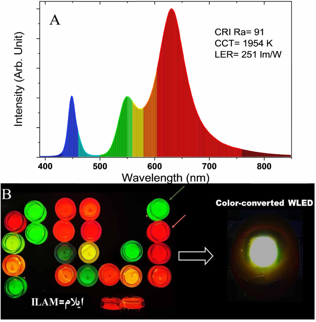
Standard image High-resolution imageWhite LEDs (WLEDs) are becoming increasingly popular due to their energy efficiency, long lifespan, and low environmental impact. They are created by combining a blue or ultraviolet LED with a phosphor material that absorbs some of the blue or ultraviolet light and emits light in the yellow or red part of the spectrum, resulting in white light.PQDs have been explored as a phosphor material for white LEDs, with CsPbBr3 QDs being coated using a one-step room temperature synthetic strategy by Guan et al [128]These QDs are stable under oxygen, moisture, and heat, and the resulting WLEDs exhibit excellent luminescent performance with a color rendering index (CRI) of 91, which is higher than most traditional WLEDs that lack red and green light components, leading to a low CRI (<80) [129] QD-WLEDs can produce a more natural-looking light that is similar to natural Sunlight, making them suitable for indoor lighting, photography, and displays with wide color gamut [130].
4.4. Applications in color conversion
QDs have a wide range of applications in color conversion, from improving display technology. QDs are heavily used in backlighting to improve the color gamut of LCDs displays. In traditional LCD displays, a white backlight is used to illuminate the display panel, and color filters are used to create the different colors of the image. However, this approach has limitations, such as a narrow color gamut and poor color accuracy. QDs can be used to improve the color gamut of LCD displays by converting the blue light from the backlight into a wider range of colors. When blue light is shone on the QDs, they emit light at a specific wavelength, determined by their size and composition. By varying the size and composition of the QDs, they can be made to emit light at different wavelengths, covering a wider range of colors. In traditional LCD displays, a white backlight is used to illuminate the display panel, and color filters are used to create the different colors of the image. However, this approach has limitations, such as a narrow color gamut and poor color accuracy. QDs can be used to improve the color gamut of LCD displays by converting the blue light from the backlight into a wider range of colors. To use QDs in backlighting, a layer of QDs is placed on top of a blue LED backlight. When the blue light from the LED backlight shines on the QDs, they emit light at specific wavelengths, producing a wider range of colors than the traditional white LED backlight. This results in a display that has a wider color gamut and better color accuracy as shown in figure 26.

Figure 26. (A) The hybridized spectrum of blue-LED and WLED with free-standing color converter film and (B) digital images of luminescent NCs and WLED fabricated by two determined NCs of green and red emission. Reproduced from [131]. © IOP Publishing Ltd. All rights reserved.
Download figure:
Standard image High-resolution image4.5. Quantum cryptography
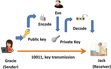
QDs have potential applications in cryptography, particularly in the field of quantum key distribution (QKD). The QKD is a method of securely distributing a secret key between two parties using the principles of quantum mechanics [132]. Moreover, QDs have been proposed as a possible source of single photons for use in QKD systems. Because of their unique optical properties, such as high brightness [133], narrow bandwidth, and long coherence time. Semiconductor-based quantum emitters are a highly promising solution for generating entangled photons on demand with near-perfect fidelity [134]. The low levels of multi-photon emission are important requirements for QKD [135]. The general architecture of QKD systems typically consists of a quantum source that generates quantum signals used to transmit the key. These signals are transmitted over the channel which could be an optical fiber or free space. At the receiving end, the quantum signals are detected and processed to extract the key information with detectors. The general architecture of the quantum key distribution is shown in figure 27.The main component of the whole system is key management which is responsible for distributing the key and ensuring secured storage. Sifted key rate is one of the important factors that needs to be taken in control. Sifted key rate is a measure of the rate at which secure key bits can be generated between two parties over a communication channel, while ensuring that the security of the transmitted information is not compromised by any third party. And a good g(2)(0) value is desirable for single photon sources as it indicates the degree of non-classical behavior of the emitted photons. A g(2)(0) value of 0 indicates perfect anti-bunching behavior, which means that the photons are emitted one at a time with no multiple photon emissions occurring at the same time. The closer the g(2)(0) value is to 0, the better the quality of the single photon source.
Figure 27. General architecture of quantum key distribution (QKD). [136].Taylor & Francis Ltd. http://tandfonline.com.
Download figure:
Standard image High-resolution image
Heindel et al [137]demonstrated the first physical experiment on free-space quantum key distribution (QKD) over a distance of 40 cm. They have used highly efficient single-photon QD sources that emit in the red and near-infrared spectrums. Information is encoded into single photons, and the security of the communication is based on the laws of quantum mechanics. Infrared light emitting devices can influence the sifted key rates by providing a source of single photons. The quality of the emitted single photons, such as their purity, coherence, and indistinguishability, can directly affect the efficiency of quantum key distribution protocols. Additionally, the photon emission rate and the spectral characteristics of the device can also play a role in determining the sifted key rate. Therefore, the performance of the infrared light emitting devices, including their g(2)(0) value and quantum bit error rate, can impact the overall quality of the sifted key rates obtained from the system. Infrared light emitting devices had sifted key rates of 27.2 kbit s−1 at a quantum bit error rate of 3.9% and a g(2)(0) value of 0.35 at moderate excitation. At higher excitation the sifted key rate of 35.4 kbit s−1 at a quantum bit error rate of 3.8% and a g(2)(0) value of 0.49. Red emitting diodes had a sifted key rate of 95.0 kbit s−1 at a quantum bit error rate of 4.1% and a g(2)(0) value of 0.49. Similar research was conducted by F Basso Basset et al [138] but over a free space distance of 250 m where they managed to share a 34.589-kB-long key string, relying on 60-bit s−1. The raw key rate with photons produced by a single QD (QD) made of GaAs that is embedded in a matrix of Al0.4Ga0.6As. The QDs are created using a technique called Al droplet etching [139]. Additionally, QDs have been utilized in creating a new type of cryptographic device called QD Cryptosystems (QDCs) which are based on the unique optical properties of QDs and the principles of quantum mechanics. These systems use the properties of QDs to create a highly secure cryptographic system that is resistant to attacks from both classical and quantum computers.
4.6. QDs-based spintronics
Spintronics has recently attracted a lot of attention as a promising area for future electronics because of its potential to improve performance and reduce energy consumption in traditional electronics. The goal of QD-based spintronics is to use the electrons' spin degree of freedom in QDs for the creation of novel electrical devices. An electron's spin, which has two conceivable values of 'up' or 'down,' can be considered as its intrinsic angular momentum. The purpose of spintronics is to develop new and more effective electrical devices by taking advantage of both the charge and spin degrees of freedom. Spintronics is anticipated to offer numerous advantages, including non-volatile data storage, quicker and more energy-efficient data processing, greater data density, and much more. Effective spin polarisation creation, transport, transfer, manipulation, and detection are necessary to fully realize the potential. These requirements are all intimately related to the material properties and as we know that QDs can confine charges due to the quantum confinement by using electrostatics the confinement potential can be controlled and the dots are even utilized for their unique electronic and optical properties, such as their strong Coulomb interaction, high tunability, and fast switching times. Spintronics is different from conventional electronics. Spintronics is based on the principle of manipulating the spin of electrons, in addition to their charge. Electrons have both charge and spin. In spintronics, the spin of electrons is used to store and process information. Unlike conventional electronics, where only the charge of electrons is used to store and process information, spintronics has the potential to offer more functionality and higher data storage capacity. This has led to the development of spin-based quantum computing [140]and novel spintronic devices such as spin-polarized light-emitting diodes, spin field-effect transistors, and spin filters. M droth et al [141]discuss various graphene QDs and their associated spin relaxation times.
5. Challenges and future prospects
Many issues need to be resolved in their development before QDs are widely used in commercial applications. A significant issue lies in the synthesis of homogeneous, high-quality QDs with stable optical characteristics. QDs may combine and produce undesired byproducts under improper synthesis circumstances, such as high temperatures and pressure. This impacts their stability and optical qualities. The development of microwave-assisted synthesis, which can significantly cut the synthesis time and enhance the yield of the QDs. The use of hybrid organic-inorganic synthesis combines both organic & inorganic precursors and can produce highly monodisperse and tunable QDs. The advent of colloidal QDs, which can be fabricated and processed in solution at mild conditions, enabled large-area manufacturing and widened the scope of QD application to markets such as consumer electronics and photovoltaics. The current synthesis techniques are mostly based on batch processes, which are time-consuming and expensive. Another key issue is the toxicity. QDs grown from heavy metals like cadmium are toxic and offer a major health concern and have an undesirable environmental effect. This restricts their usage in biological and medical imaging. To address this challenge, researchers are exploring alternative materials and synthesis methods that can produce non-toxic QDs with similar or better properties. To mitigate the potential toxicity of traditional QDs, one effective approach is to modify their core–shell structure using biocompatible ligands or polymers. This can help to reduce the negative effects of toxicity. Traditional Cd-based QDs can be harmful to cells due to their toxicity and ability to cause DNA damage. However, this toxicity can be mitigated by applying a protective coating made of polymers to the surface of the core QD. This coating serves to prevent the release of heavy metal ions from the interior of the QD, thus improving its stability and reducing its toxicity [142]. While carbon based QDs have garnered attention for their potential use in bioimaging, a major obstacle is creating CQDs that can emit in the long-wavelength range and be used with various imaging modes. To address this, researchers have developed bismuth- and gadolinium-codoped CQDs (Bi,Gd-CQDs) using a hydrothermal approach. These Bi,Gd-CQDs are capable of producing multiple colors of fluorescence, making them suitable for use in cell imaging [143]. Before using QDs in real applications, it is necessary to address the compatibility with various materials. Moreover, there have been constant efforts to enhance the optical and electronic properties of QDs.
In QD-LEDs the important characteristic is the EQE which generally decreases due to the droop phenomenon as discussed above. To solve the issue of droop in light-emitting devices, two approaches have been taken: optimizing the device design and controlling the structure of QDs. QD multishell heterostructures have been found to be effective in reducing Auger recombination by creating a uniform confinement potential that limits the intergap transition. This enabled red-emitting LEDs with high droop-free EQEs up to ~100,000 cd m–2 [144]. The narrowband emission by QDs compared with other semiconductors is an added advantage for next generation displays. QDs that have been patterned are utilized as a photoactive substance which absorbs blue light of short wavelengths and emits light of longer wavelengths in blue, green, and red colors. This eliminates the need for separate color filters, which results in higher device efficiency and light output while reducing color cross-talk and even reduces the number of layers in the device stack [145]. To address the issue of energy consumption in lighting, solid-state WLEDs are being considered as a promising source of illumination due to their improved efficiency, energy-saving capabilities, and environmental friendliness. A simple and effective approach to improve the luminescence and stability of CsPbBr3 QDs is to modify their ligands. Using ideal ligands that bind more strongly to the surface, such as propanesulfonate and alkyl phosphonic acids, can enhance the performance of these QDs [146]. A highly efficient production of red and green QDs is crucial for achieving a high color rendering index (CRI) value for warm WLEDs, making it an attractive strategy.
QDs have shown great promise in the field of solar energy as they can be used to create more efficient solar cells. Lead-based QDs have wide applications in solar cells due to high power conversion efficiency and broad absorption spectrum. For instance, nea-infrared (NIR) PbS QDs based solar cells demonstrate almost 12% conversion efficiency [147].
New materials are being developed to enhance the optoelectronic capabilities of QDs including perovskite and metal-organic framework (MOF) QDs. These MOF-QDs can potentially be used as a sensor to detect harmful contents like Mercury (Hg) in water [148]. This replaces all the traditional QDs which are toxic and not very stable in water like solvents and can be further used as an alternative to techniques such as Atomic Absorption Spectroscopy which is very time-consuming and requires sophisticated instrumentation. Emerging technologies including the Internet of Things (IoT) with interesting outcomes are expected to come from the integration of QDs with IoT in the healthcare industry. The new dimension of QD applications involves hospitals, pathological labs [149], artificial intelligence (AI), and quantum computing.
6. Conclusion
In conclusion, QDs have gained significant attention due to their unique properties and potential applications in various fields such as bio-medical, optoelectronics, quantum cryptography, and spintronics. The synthesis and characterization of QDs have made significant progress over the years, ranging from colloidal synthesis to molecular beam epitaxy and biomimetic synthesis. The advancements in the synthesis of QDs have resulted in improved optical and electronic properties of these nanomaterials. The application of QDs in various fields has shown promising results and has opened up new avenues for research and development. However, there are still some challenges that need to be addressed to further advance the field of QDs. Despite the challenges, the future prospects of QDs are bright and they are expected to play a major role in the advancement of various fields. Overall, QDs are an exciting area of research and have the potential to bring about significant advancements in various fields.
Data availability statement
No new data were created or analysed in this study.