

Abstract
In recent years, with the continuous development of solar blind ultraviolet photodetectors, III-V compounds are widely used as semiconductor materials. The nanowire array structure has excellent 'light trapping effect'. However, if the distance of nanowire is too close, the secondary absorption problem of the nanowire will occur. If the distance of nanowire is too far, the number of photocarriers generated in the nanowire array per unit volume will be reduced. Meanwhile, the absorption capacity of the nanowire structure with different shapes is different. Based on this background, we studied the influence of the period and geometry of AlGaN nanowires with different Al components on the optical response properties. The finite time domain difference (FDTD) method was used to compare the quantum efficiency and collection efficiency of AlGaN nanowires with different Al components, we found that the quantum efficiency of the hexagonal nanowire array with Al component of 0.42 is as high as 45%, which is the highest in our structure. At the same time, its cutoff wavelength is at 280 nm, which has excellent solar blindness. Therefore, the study in this paper can provide some theoretical reference for the experiment and preparation of AlGaN photocathode.
Export citation and abstract BibTeX RIS

Original content from this work may be used under the terms of the Creative Commons Attribution 4.0 licence. Any further distribution of this work must maintain attribution to the author(s) and the title of the work, journal citation and DOI.
1. Introduction
Ultraviolet radiation is an important component of solar radiation. The earth's ozone layer can absorb ultraviolet radiation below 290 nm in sunlight. As a ternary compound semiconductor material, AlGaN has a continuously adjustable band gap between 3.4 eV and 6.2 eV. AlGaN semiconductor materials have excellent photoelectric properties in the ultraviolet region. At the same time, the existence of ozone layer also provides high quality detection background for AlGaN ultraviolet devices [1–3]. Ultraviolet devices based on AlGaN materials have the advantages of small volume, stable operation, low operating voltage, high sensitivity, high efficiency, working in the blind area and so on [4–6]. Huang et al established a demonstration imaging system with AlGaN solar blind/visible blind dual-band detector components as the core, and verified the good band selectivity of AlGaN UV detector through experiments [7]. In 2006, Serkan Butun et al prepared and tested an AlGaN photodetector with MSM structure with Al component up to 0.75, which has met the requirements of solar blind ultraviolet detection [8]. Liu et al studied the optical properties and quantum efficiency of AlGaN quantum well on AlGaN and AlN, and found that the quantum well on AlGaN substrate has better optical gain, which indicates that AlGaN substrate has a broad application prospect in efficient deep ultraviolet lasers and light-emitting diodes [9]. Therefore, AlGaN semiconductor materials have a wide range of application prospects.
In recent years, with the development of nanostructures, nanowire arrays (NWAs) have been widely studied. Because of its light trapping effect, NWAs significantly increases the light absorption of photocathode, thus improving the photoelectric conversion efficiency of photocathode [10–13]. Wafaa K khalef et al Measured the maximum quantum efficiency of 92% at an applied voltage of 1 V by growing ZnO nanowires on silicon and quartz substrates in 2020 [14].Chen et al designed and fabricated a novel self-powered nano-structured UV detector using the sno2-tio2 nano-heterostructure as the photoanode. The uv detector has fast light response speed, high photosensitivity and good spectral selectivity [15]. The advantage of NWAs photocathode is that the absorption coefficient of the material is higher in the short wavelength, and the photon absorption depth is shallower. Meanwhile, electrons can escape from all the surface of the nanowires, and the electrons at the inner edge of the nanowires are easier to emit. However, the photocathode side of the film surface does not emit electrons, so the electron overflow probability is lower than that of NWAs [16–18]. It was just based on this background that the article was written. The finite time domain difference (FDTD) method is used to measure the maximum possible light absorption and quantum efficiency of AlxGa1−xN nanostructures with different Al components. Prior to this, there have been many studies on light absorption based on FDTD nanostructures. For example, GaN truncated nanocones, proposed by Yeong Jae Kim et al, could achieve higher solar water decomposition efficiency [19]. Zhang et al used FDTD to compare the light absorption of different GaAs nanostructures and found that the nanocone array achieves the highest photoelectric conversion efficiency when the diameter/period ratio is 0.72 [20].
Therefore, in the work of this paper, AlGaN with different Al components is the main nanowire array material used in this paper. Since the working wavelength of the solar blind UV detector is between 200–280 nm [21], it is best for us to select the cut-off wavelength within this range when selecting materials, and the cut-off wavelength of materials is related to the width of the band gap. Eg(GaN) = 3.42eV, Eg(Al0.42Ga0.58 N) = 4.37 ev,Eg(Al0.49Ga0.51 N) = 4.56 eV,Eg(Al0.66Ga0.34 N) = 5.05 eV, Eg(AlN) = 6.2 eV. Their cut-off wavelengths correspond to 362.57 nm(GaN), 283.75 nm(Al0.42Ga0.58 N), 271.93 nm(Al0.49Ga0.51 N), 245.40 nm(Al0.66Ga0.34 N) and 200 nm(AlN) respectively [22]. This basically covers the solar blind ultraviolet range. So we choose AlGaN with Al components of 0, 0.42, 0.49, 0.66 and 1 as the nanostructure material. We use the finite time domain difference (FDTD) method to simulate the difference of absorption rate of different nanostructures or different nanomaterials under the same parameters, and obtain different quantum efficiency and collection efficiency through absorption rate calculation, so as to study the influence of different nanostructures of different Al components on the quantum efficiency and absorption efficiency. This research provides a possible way to improve the photoelectric performance of solar blind ultraviolet detectors.
2. Model and simulation
2.1. Quantum efficiency
The schematic diagram of AlGaN thin film photocathode is shown in figure 1(a). In one dimensional space, when the vertically incident plane wave acts on the surface of the film, the incident photon with energy will generate photocarriers in the film, and these carriers will diffuse to the surface of the film under the action of concentration gradient. The quantum efficiency formula of reflective thin-film photoemission materials can be obtained by solving the one-dimensional carrier continuity equation:


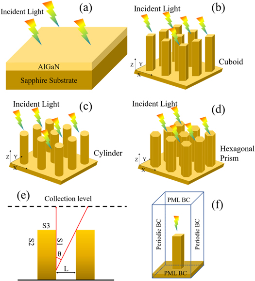
Figure 1. (a) Three-dimensional structure of the light absorption of the AlGaN thin film, (b) Three-dimensional structure of the light absorption of the AlGaN Cuboid nanowire array. (c) Three-dimensional structure of the light absorption of the AlGaN cylinder nanowire array. (d) Three-dimensional structure of the light absorption of the AlGaN hexagonal prism nanowire array. (e) Schematic diagram of electron ejection. (f) Three-dimensional domain unit of the AlGaN NWAs.
Download figure:
Standard image High-resolution imageAmong them,  is the diffusion coefficient of carriers in AlGaN nanomaterial,
 is the incident photon flux density,
  is the concentration of the carrier at x,
  is the lifetime of the carrier,
 is the photon flow density, P is the probability of surface escape, P = 0.7,
  is the absorption coefficient, R is the surface reflectivity,
  is the electron diffusion length,
  The absorption coefficient can be obtained by the extinction coefficient K

According to Formula (4), curves of different absorption coefficients with wavelength can be calculated. After obtaining the quantum efficiency of the reflection film photocathode, we extend the one-dimensional carrier continuity equation to two dimensions [23].


Where,  and
and  are carrier density functions, H is nanowire height. According to one top surface, one back interface and two sides of the nanowires, four boundary conditions can be obtained:

Where,  and
and  are the sum of two side electron emission and interface recombination rates respectively,
  is the sum of top electron emission and interface recombination rates,
  is the back interface recombination rate,
  Thus, we can calculate the quantum efficiency component of each emission surface through the surface emitted carrier concentration, and finally calculate the total quantum efficiency [24]

Among them,  is the diffusion coefficient of carriers in AlGaN nanomaterial, P is the probability of surface escape,
  is the incident photon flux density, H is the surface area irradiated by incident light.
For the nanowire array structure, the photoelectrons emitted from the side of the nanowire may be absorbed by the adjacent nanowire and thus cannot escape from the array. In this case, the quantum efficiency is no longer able to perfectly evaluate the photoelectric performance of the nanowire array. So we introduce the collection efficiency to actually evaluate its photoelectric conversion efficiency, as shown in figure 1(e). Since the photoelectrons emitted from the top surface S3 of the nanowire are generally considered to be completely absorbed by the collecting end, the collection efficiency of the top surface is 1 by default. The collection probability of S1 and S2 on the side of nanowire array satisfies the formula [25]

Where,  is the normalization coefficient of Henke modal distribution,
  A is the normalization coefficient,
  is the initial energy of the photoelectron,
  is the elevation angle of the photoelectron, L is the spacing of nanowires.
Thus, we can derive the collection efficiency formula of the photocathode of the nanowire array

2.2. Structural simulation
Figure 1 shows the schematic diagram of AlGaN nanostructures of different Al components we studied. In figure 1(a), we set the height of the film as 400 nm and the height of the sapphire substrate as 250 nm, and the period of both the film and the sapphire substrate is 300 nm. In figure 1(b), we set the height of the cuboid nanowire array as 400 nm, the length and width of the top and bottom are D1, and the period is P. In figure 1(c), we set the height of the cylindrical nanowire array as 400 nm and the diameter of the top and bottom as D2. In figure 1(d), we set the height of hexagonal prismatic nanowire array as 400 nm, and the top and bottom side lengths as D3. After the structural parameters of AlGaN nanowire array were defined, we began to compare the absorptivity and quantum efficiency of AlGaN materials with different Al components and different nanostructures. The refractive index n and extinction coefficient K of Al component x = 0, x = 1 and Al component x = 0.42, x = 0.49, x = 0.66 were respectively obtained from the experimental data of AB Djurišić et al [26] and Whale et al [27].
Figure 2 shows the curves of refractive index n and extinction coefficient K of AlGaN materials with different Al components in reference as incident wavelength changes. In addition, since we cannot obtain the refractive index between 200–300 nm for some Al component AlGaN materials, we adopt spline fitting function to obtain the refractive index between 200–400 nm. We evaluated the optical absorption properties of solar spectral wavelengths ranging from 200 to 400 nm, covering the solar blind band (200–280 nm), and the extinction coefficients of AlGaN materials we selected decreased to 0 after 400 nm. Therefore, plane waves with a wavelength range of 200–400 nm defined by the power intensity and wavelength values from the discrete AM 1.5 g solar spectrum were selected to simulate the incident sunlight.

Figure 2. Refractive index (left) and extinction coefficient (right) of AlGaN materials of five different Al compositions.
Download figure:
Standard image High-resolution imageIn this paper, FDTD is mainly used to simulate the optical properties of different nanostructures shown in figure 1(a), (b), (c) and (d). After the nanowire model was built, DFTD boundary was set. As shown in figure 1(f), to simulate the AlGaN nanowire array with periodic structure, periodic boundary conditions are applied to the x and y direction boundaries, and perfect matching layer (PML) boundary conditions [28] are applied to the axial boundaries to absorb all incident light energy. Then we use MATLAB software based on the finite difference method to establish the calculation model of different Al components and different nanowire array structures, so as to obtain their quantum efficiency and collection efficiency.
3. Results and discussion
In order to study the influence of AlGaN material with different nanowire array periods on optical properties, we set up the thin film structure and nanowire array structure with different periods, as shown in figures 1(a) and (b). Al0.66Ga0.34 N nanomaterial is used as photocathode material, the total height is H = 400 nm, sapphire is selected as the substrate, and the distance between the plane wave and the top of the nanowire is 600 nm. Figure 1(a) shows the thin film nanostructure. Figure 1(b) shows the cuboid nanowire array structure. The length and width of the nanowire are both 100 nm. We set the nanowire periods of 125, 150, 175, 200 and 250 nm respectively. Figure 3 shows the comparison of incident light absorption between the thin film nanostructure and the cuboid nanowire array structure.

Figure 3. Comparison of absorptivity between thin films and nanowire arrays with different periods.
Download figure:
Standard image High-resolution imageFrom the simulation results, we can find that when the nanowire period is between 125 nm–200 nm, the light absorption characteristics of the nanowire array structure are obviously better than that of the thin film structure. This is mainly due to the 'light trapping effect' of the nanowire array, which improves light absorption. At the same time, we can also find that when the period of nanowire array is 150 nm, its absorption rate in the wavelength range of 200–400 nm is better than other periods. And it is sensitive to the selection of wavelength, before 295 nm, its absorption rate is more than 85%, after 295 nm, its absorption rate begins to decline significantly, which meets the requirements of semiconductor materials for making ultraviolet detectors. Therefore, 150 nm was selected as the period of nanowire array in the simulation of different AlGaN nanowire array structures.
In order to study the influence of nanowire array structure of AlGaN materials with different Al components on optical properties, cuboid nanowire array structure, cylindrical nanowire array structure and hexagonal prism nanowire array structure of AlGaN materials with different Al components are set up, as shown in figures 1(b)–(d). Height H = 400 nm, period P = 150 nm, sapphire substrate is selected, and the distance between the light source and the top of the nanostructure is 600 nm. Figure 1(b) shows the cuboid nanowire array structure, whose length and width are d1 = 100 nm. Figure 1(c) shows the cylindrical nanowire array structure, whose diameter is d2 = 100 nm. Figure 1(d) shows the hexagonal prism nanowire array structure, and the side length of the nanowire is d3 = 50 nm.
The finite time domain difference (FDTD) method was used to simulate these three models, and their reflectivity and transmittance were obtained respectively. Absorption rate of each model was obtained through calculation. Absorption rate curve is shown in figures 4(a)–(c). It can be observed from figures 4(a)–(c) that in the nanowire array structure, with the increase of Al component, the cutoff wavelength of the nanowire appears blue shift, while its absorption rate gradually decreases.

Figure 4. (a) Absorption rates of cuboid nanowire arrays of different Al components. (b) Absorptivity of cylindrical nanowire arrays of different Al components. (c) Absorption rates of hexagonal prismatic nanowire arrays of different Al components.
Download figure:
Standard image High-resolution imageAccording to figures 5(a)–(e), it can be observed that the cutoff wavelength of the nanowire also changes with the change of the structure of the nanowire array. When the nanowire array structure changes from cuboid to cylinder and then to hexagonal prism, the cutoff wavelength appears blue shift. This is mainly because in the hexagonal prism structure, the axial distance from the central point to the periphery is  at the shortest and 50 nm at the longest. In the cylindrical structure, the axial distance from the center point to the periphery is 50 nm. In the cuboid structure, the axial distance from the center to the periphery is the shortest 50 nm and the longest
  At this point, the electrons inside the nanowires need higher energy to escape from the nanowires, that is, the electrons need to escape from the nanowires under the irradiation of higher energy, so the wavelength blue shift appears.

Figure 5. (a) When Al component is 0, the absorption rate of nanowire array. (b) When Al component is 0.42, the absorption rate of nanowire array. (b) When Al component is 0.49, the absorption rate of nanowire array. (d) When Al component is 0.66, the absorption rate of nanowire array. (e) When Al component is 1, the absorption rate of nanowire array.
Download figure:
Standard image High-resolution imageAnd it can be observed that in the short-wavelength region, the absorption rate of hexagonal prism nanowire array is slightly higher than that of cuboid and cylinder. In the long wavelength region, the absorption rate of cuboid nanowire array is slightly higher than that of cylindrical and hexagonal prism.
After simulation analysis of absorption rate of nanowire array, data analysis of internal carrier concentration and quantum efficiency is carried out. By observing figure 2., we can find the relationship between extinction coefficient and wavelength, and draw a conclusion: extinction coefficient K decreases gradually with the increase of wavelength, and extinction coefficient K also decreases gradually with the increase of Al component until it decreases to 0. When the extinction coefficient decreases to 0, the corresponding wavelength becomes smaller and smaller. The quantum efficiency and collection efficiency can be solved only after the absorption coefficient is obtained by calculation. When the absorption coefficient is 0, the quantum efficiency value obtained is small and basically has no reference value. In addition, when the absorption coefficient is 0, the quantum efficiency does not change with wavelength. In practical application, AlGaN nanowire array is mainly used in ultraviolet devices, so for ultraviolet detectors, we mainly consider their response characteristics in hyperspectrum. Therefore, we only conduct data analysis on the part with extinction coefficient greater than 0 to study the quantum efficiency of different nanostructures.
For the photocathode of nanowire array structure, the quantum efficiency can only represent the probability of photogenerated carriers generated in the nanowire. Due to the array arrangement of nanowire, the photogenerated carriers generated on the side of the nanowire emit around, causing some of the carriers to be absorbed by the adjacent nanowire and unable to be collected. collection efficiency is introduced to evaluate the photogenerated carrier probability actually available for nanowire arrays. Because the side length of the cuboid is 100 nm and the height is 400 nm; The diameter of the cylinder is 100 nm and the height is 400 nm; The hexagonal prism has a side length of 50 nm and a height of 400 nm. The two-dimensional cross sections of the three structures on the xoz plane are rectangular with a width of 100 nm and a height of 400 nm, so we use the same photoelectric emission model to calculate their 2d quantum efficiency and collection efficiency.It can be observed from figures 6(a)–(c) and 7(a)–(c) that the quantum efficiency and collection efficiency of nanowire array also change with the change of Al component. In different AlGaN materials, with the decrease of Al component, the quantum efficiency and collection efficiency of nanowire array gradually increase, and its cutoff wavelength moves to the direction of long wave. When the Al component is 0.42, in different nanostructures, it has ultraviolet cutoff wavelength and its quantum efficiency reaches the maximum.

Figure 6. (a) Quantum efficiency of cuboid nanowire arrays of different Al components. (b) Quantum efficiency of cylinder nanowire arrays of different Al components. (c) Quantum efficiency of hexagonal prism nanowire arrays of different Al components.
Download figure:
Standard image High-resolution image
Figure 7. (a) Collection efficiency of cuboid nanowire arrays of different Al components. (b) Collection efficiency of cylinder nanowire arrays of different Al components. (c) Collection efficiency of hexagonal prism nanowire arrays of different Al components.
Download figure:
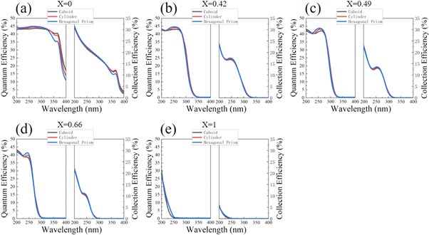
Standard image High-resolution imageWhen we observe the quantum efficiency of cuboid, cylinder and hexagonal prism nanowire arrays with the same Al component, as shown in figure 8, it can be found that their quantum efficiency and collection efficiency change little in the ultraviolet band. The speculation may be due to the fact that we used the same Spicer 'three-step model' theory to calculate the quantum efficiency and collection efficiency of different nanowire array structures. Meanwhile, we calculated the quantum efficiency and collection efficiency through the absorption rate of nanowire array. As we can see from figure 5, the absorption rate of the three different structures did not change significantly, so did the quantum efficiency and collection efficiency of the three structures. The quantum efficiency and collection efficiency change from cuboid and cylinder to hexagonal prism, and their cut-off wavelength gradually shifts blue. According to figure 8(b), when the Al component is divided into 0.42, the hexagonal prism nanowire array has the maximum quantum efficiency in the ultraviolet band, and its cutoff wavelength is at 280 nm, which matches the working band of the solar blind ultraviolet detector. Therefore, Al0.42Ga0.58 N hexagonal prism nanowire array with side length of 50 nm is considered to be the most suitable photocathode for ultraviolet detectors.
Figure 8. (a) Quantum efficiency(right) and collection efficiency(left) of GaN with three structures. (b) Quantum efficiency(right) and collection efficiency(left) of Al0.42Ga0.58 N with three structures. (c) Quantum efficiency(right) and collection efficiency(left) of Al0.49Ga0.51 N with three structures. (d) Quantum efficiency(right) and collection efficiency(left) of Al0.66Ga0.34 N with three structures. (e) Quantum efficiency(right) and collection efficiency(left) of AlN with three structures.
Download figure:
Standard image High-resolution image
4. Conclusion
By comparing the absorbance of the same structure in different periods, we found that the absorbance of thin film was lower than that of nano wire. When the diameter is 100 nm, the absorptivity of the nanowire array with a period of 150 nm is the best. All the structural geometric parameters of nanowire arrays in this paper are set based on this premise. In the comparison of absorptivity of AlGaN nanowire arrays with different Al components,, we found that the cutoff wavelength of the nanowire array showed a blue shift with the increase of Al components. When the Al component is 0.42, the cutoff wavelength is about 280 nm, and the Al0.42Ga0.58 N material has the best wavelength selectivity. At the same time, we found that the quantum efficiency and collection efficiency based on the two-dimension nanowire array are proportional to the absorption rate. Finally, when comparing cylindrical nanowires, rectangular nanowires and hexagonal nanowires with the same geometric parameters, it is found that there is little difference in quantum efficiency among the three nanowire array structures, but the cutoff wavelength of hexagonal nanowire arrays is closer to 280 nm. Therefore, Al0.42Ga0.58 N hexagonal prism nanowire array with height H = 150 nm, diameter D2 = 100 nm and period P = 150 nm has the most suitable quantum efficiency spectrum. However, the quantum efficiency and collection efficiency are calculated based on the two-dimensional plane in this paper, which cannot fully represent the three-dimensional meter line array structure. Therefore, the three-dimensional quantum efficiency and collection efficiency algorithm of nanowire array structure need to be further improved. However, the AlGaN nanowire array structure with good cut-off characteristics obtained in this paper may be helpful to the study of high quantum efficiency photocathode in far ultraviolet band.
Acknowledgments
This work is sponsored by Natural Science Foundation of Jiangsu Province-China (Grant No. BK20211193) and LLL Night Vision Technology Key Laboratory Fund (Grant No. J20210103).
Data availability statement
All data that support the findings of this study are included within the article (and any supplementary files).