
Abstract
The characterisation of dielectric-semiconductor interfaces via Kelvin probe surface voltage and photovoltage has become a widespread method of extracting the electrical properties influencing optoelectronic devices. Kelvin probe offers a versatile, contactless and vacuum-less technique able to provide useful insights into the electronic structure of semiconductor surfaces. Semiconductor theory has long been used to explain the observations from surface voltage measurements, often by making large assumptions about the characteristics of the system. In this work I report an updated theoretical treatment to model the results of Kelvin probe surface voltage and photovoltage measurements including four critical mechanisms: the concentration of charge stored in interface surface states, the charge stored in different locations of a surface dielectric thin film, the changes to effective lifetime and excess carrier density as a result of charge redistribution, and the non-uniformity of charge observed on most large scale thin film coatings used for passivation and optical improvement in optoelectronic devices. A full model is drawn and solved analytically to exemplify the role that these mechanisms have in surface voltage characterisation. The treatment in this work provides crucial understanding of the mechanisms that give rise to surface potential in semiconductors. As such this work will help the design and development of better optoelectronic devices.
Export citation and abstract BibTeX RIS

Original content from this work may be used under the terms of the Creative Commons Attribution 4.0 licence. Any further distribution of this work must maintain attribution to the author(s) and the title of the work, journal citation and DOI.
1. Introduction
Kelvin probe (KP) characterisation of surface voltage in semiconductors has recently seen a resurgence despite the technique having been around for many decades [1–3]. This renewed interest seems to be due to the development of instruments capable of accurately detecting millivolt range changes in the surface potential of semiconductors, without requiring contacts or a vacuum, and using probes in the micron to millimetre scale [4]. KP allows contactless measurements of work function differences between metals, or surface potential differences for non-metals. The technique can be also used to measure the surface potentials of dielectrics thin films deposited on top of semiconductors, with the measured contact potential difference (CPD) being strongly dependent on the presence of charge in andon the dielectrics [5]. Thanks to these capabilities the KP method [6] has become more widespread in the photovoltaics (PV) and optoelectronics field, including the large community studying perovskite solar cells [7, 8], as well as groups working on silicon devices [9–15], and other thin film technologies [16, 17]. The working principles of KP have long been reported and used in commercial instruments. References [1, 6, 18, 19] have a comprehensive account of the fundamental theory and instrumentation behind KP instruments. It is noted that the KP referred to here is not that based on scanning probe microscopes, also known as scanning Kelvin probe force microscopy (SKPFM). The KP referred to here is a  to
to  scale instrument.
An extension of the KP technique is the use of illumination to induce changes to the surface voltage (SV) of the semiconductor due to the creation of electron-hole-pairs (EHP) at the surface. Termed surface photovoltage (SPV), the effect is the result of charge redistribution within the semiconductor under illumination. Since the semiconductor will interact with light differently depending on the wavelength and intensity of the light, these parameters can be varied in the surface photovoltage technique to investigate specific phenomena. For example, the illumination can target sub bandgap states by using IR low energy light, or it can also look at near-surface absorption of photons using short wavelength, high intensity UV light. Altogether this family of methods is known as surface photovoltage spectroscopy. The most notorious change in a semiconductor under illumination is the reduction of its surface potential. In the dark, the semiconductor surface will present a space charge region (SCR) due to the concentration of charge in surface states and in the dielectric, which are in turn mirrored by opposite charge carriers in the semiconductor. This SCR creates a built-in potential right at the surface of the semiconductor. Under illumination the amount of surface potential required to mirror interface and dielectric charge reduces as the free carrier concentration increases from optically injected EHP. Changes to surface potential can be detected as a function of wavelength, intensity, timed illumination pulses, or steady state illumination, and can be used in conjunction with semiconductor theory to extract a variety of device and material properties [19].
The theory behind how a surface voltage originates from changes in a semiconductor surface coated with a dielectric thin film has been covered in length, for example in [19–22]. In brief, surface voltage results from difference between the absolute electrostatic potential of the measuring probe, and the electrostatic potential of the semiconductor surface given by the semiconductor work function and the presence of any charge both at the semiconductor near-surface and in the dielectric thin film. When combined with light excitation, the detected changes in surface voltage can be used to extract minority carrier diffusion lengths [23, 24], barrier heights [25], flat-band voltages [26], interface trap density [27], and effective lifetimes [28]. While theories used to understand KP surface voltage and extract such parameters have worked well under a set of assumptions, new understanding of the charging and inhomogeneity effects at semiconductor-dielectric interfaces have recently come to light [29, 30]. To date, a model and solution algorithm has not yet been produced to explain surface voltage and photovoltage measurements of dielectric-semiconductor interfaces when accounting for the combined effects of:
- 1.Charge stored in interface defect states. At the interface between a semiconductor and another material there arise bandgap states that originate from the disruption to the crystallographic lattice. These states can have both donor and acceptor nature and as such they can store a concentration of charge, which is dependent on the surface potential and quasi-Fermi level position at the semiconductor surface.
- 2.Charge stored in the surface dielectric layer. Dielectric thin films often present a concentration of embedded charge, and this charge can vary in position and concentration making it a function of thickness and depth into the dielectric.
- 3.The effective carrier lifetime of the semiconductor and its dependence on surface charge and illumination. When using the surface photovoltage technique several assumptions are made to what the excess minority carrier density is at the surface of the semiconductor. Often informed by the absorption coefficient at the incident wavelength, these assumptions can lead to large errors in predicted SPV values since the minority carrier density depends on the surface passivation which in turn is wavelength, generation intensity, and charge dependent.
- 4.Charge fluctuations at the surface of the dielectric. While most modelling approaches use a one-dimensional analysis, the concentration of charge and interface states have been recently reported to show large non uniformities leading to dispersion in the physical quantities measured [30].
This manuscript reports a model that includes all these mechanisms and provides a useful tool to understand KP measurements of dielectric-semiconductor interfaces.
2. Surface voltage in the dark
In the following the basic concepts involved in the calculation of CPD in the dark are explained in detail as they form the basis of the complete model in this work. The concepts are developed focusing on the dielectric - n-type silicon system. Figure 1 shows a schematic picture of the system, including an energy band diagram, and an exemplary carrier densities and charge concentration across the structure, in a one-dimensional representation. Figure 1(a) represents the case where positive charge is present in the dielectric and thus it generates an excess electron concentration ( at the semiconductor surface, in contrast to the carrier bulk concentrations (
 ). This produces a positive amount of surface potential
  Conversely figure 1(b) illustrates the case where a negative concentration of charge creates excess hole concentration at the surface (
 leading to an inversion region and a large negative surface potential
  Critically, this diagram pictures the effect of the donor- and acceptor-like interface state densities (
 ). In figure 1 these are pictured in blue for donor-like states since they become positively charge as they release an electron, and yellow for acceptor-like states gaining an electron when ionised. Since a charge concentration Qit
is stored in these interface defect states, they influence the charge distribution across the interface. Occupational statistics need to be solved in order to calculate the concentration of interface charge (
). In figure 1 these are pictured in blue for donor-like states since they become positively charge as they release an electron, and yellow for acceptor-like states gaining an electron when ionised. Since a charge concentration Qit
is stored in these interface defect states, they influence the charge distribution across the interface. Occupational statistics need to be solved in order to calculate the concentration of interface charge ( ), as well as SCR charge density in the silicon (
 ). It is also noted that
  is a function of energy, with a marked increase in available energy states towards both ends of the bandgap, termed the band tails [31]. This is pictured in the left pointing
  axes on the left of each figure, with the blue and yellow-filled rectangles indicating the presence of positive and negative charge at the interface, respectively.

Figure 1. Schematic diagram of insulator—semiconductor interface including the band structure for the case where (a) there is positive charge in the insulator, and (b) there is negative charge in the insulator. 

 indicate the conduction, valence and Fermi energies in the system.
Download figure:
Standard image High-resolution imageIn Kelvin probe measurements the oscillating tip is held at a metal voltage  and it is varied with respect to a grounded semiconductor bulk with local potential determine by its work function Φs
. KP measurement then determine the contact potential difference (CPD) required to bring the semiconductor to the same electrical potential as the Kelvin metal probe. Under an external voltage
and it is varied with respect to a grounded semiconductor bulk with local potential determine by its work function Φs
. KP measurement then determine the contact potential difference (CPD) required to bring the semiconductor to the same electrical potential as the Kelvin metal probe. Under an external voltage  applied to a metal probe sitting above the semiconductor, the potential difference between them can be calculated by adding the electrostatic potentials involved as:

Where Φm/s are the local work functions for the metal and the semiconductor respectively [19],  is the potential drop across the insulator [32], and
  is the surface potential due to the SCR.
Kelvin probe determines the applied metal voltage that equalises potential between the metal and the semiconductor bulk, such that  V = 0, and the contact potential difference

Where Φms
is the work function difference between the metal and the semiconductor, given in eV units, and  is the electron elementary charge. The work function of metals has been well researched in the past [33]. The semiconductor work function is defined in terms of the doping concentration and type since the Fermi energy depends on doping, as:

Where  is the electron affinity, and
  is the semiconductor bandgap. The Fermi energy:

is positive for n-type and negative for p-type semiconductors,where  is the temperature-dependetent semiconductor intrinsic carrier concentration,
  is the dopant concentration,
  is the temperature, and
  the Boltzmann constant.
The insulator voltage  is calculated in a similar way to the flat-band shift in an MIS structure extending to any charge density (
 ) that can appear both in the insulator or in the air gap between the sample and the KP metal tip [33]:

where  is the relative permittivity of the insulator,
  the gap distance between the sample and the metal tip normally in air, and
  the volumetric concentration of charge in the insulator and the air gap. Since under good experimental conditions there is no charge concentration in the air, the insulator potential reduces to:

It is not possible to know the exact distribution of charge within the dielectric film. It is hence convenient to represent the charge as an effective fixed sheet charge density  centred at a plane a distance
  from the insulator-silicon interface, for which the argument of the integral can be solved by equating a delta Dirac function at
 The location of the charge
  is termed the centroid of the charge concentration. The insulator potential drop is then given by:

The KP CDP in the dark can hence be found as:

Often the insulator capacitance  is known from a different characterisation technique, so that the CPD can be rewritten as:

To determine the semiconductor SCR potential  it is necessary to follow an iterative algorithm that finds the charge neutrality condition given by sum of the charge concentration in insulator, interface states and semiconductor space charge region. Previous works that characterise charge concentration in dielectrics often disregard
  as it has small contributions when the dielectric is thick, and the charge centroid
  is large. Here
  will be always considered as it includes the crucial information on the occupation of interface states when the charge centroid is close to the dielectric-silicon interface. A calculation of
  is achieved by following an iterative procedure outlined by Girisch et al [34], and extended by Aberle et al [35] to include the steady-state generation of minority carriers by illumination. Since this procedure is applicable to the case of surface photovoltage it will be treated in the next section.
3. Surface voltage under illumination
The injection of light into the semiconductor causes a change to the distribution of charge in the system. Most notoriously the amount of semiconductor surface potential changes as the occupation statistics for bandgap and valence and conduction band states are now determined by the quasi-Fermi energies in the region injected with light. The initial physical quantity that must be considered is the generation current created by the illumination source. A low-cost and versatile alternative for carrying out SPV measurements is the use of a bright halogen light source that can inject substantial carrier concentrations, often to the point where it is possible to assume  V. Alternatively it is possible to use high intensity lasers to produce large concentrations of carriers at a desired depth into the semiconductor, depending on its absorption coefficient. For the purposes of determining the generation current, let us consider a halogen light with the spectrum pictured in figure 2(a). Such light can be placed at 45° angle from the specimen's axis, and for example provide an intensity of
  50 mW cm−2 at the specimen's surface. The optical characteristics of the specimen must be known in order to find out the amount of reflection, transmission and absorption taking place. For exemplification let us consider a 200 μm thick n-type silicon specimen, coated with a thermally grown layer of SiO2 100 nm thick. An optical simulator or ray tracer can be used to calculate the generation rate at the near-surface region of the semiconductor as depicted in figure 2(b). In this example the rapid optical simulator OPAL2 has been used [36], using the implementation published in [37]. Since the modelling in this work follows Girisch and Aberle's algorithm, the excess carrier density is assumed to be constant in the space charge region, and thus an average generation rate must be used. In the case of the example pictured in figure 2(b), the average generation rate close to the surface is in the order of 1019 cm−3s−1.
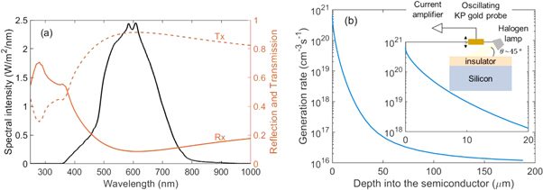
Figure 2. (a) Spectrum for halogen light often used in KP surface photovoltage characterisation including transmission and reflection when light shines at 45° on the example Si-SiO2 system. (b) Generation rate for a 45° light injection with intensity  50 mW cm−2, as a function of depth for a silicon specimen with a 100 nm SiO2 thin film on top.
Download figure:
Standard image High-resolution imageAnother practical method of determining the average generation rate is to conduct sheet resistance ( ) measurements of the specimen when irradiated with the same intensity of light as done in the SPV experiment. One such measurements will produce a value of sheet resistance in the dark
  and under illumination
  which can then be used to find the corresponding generation rate required to produce a similar change in sheet resistance. This requires knowledge of the electrical properties of the sample, but not the optical properties. For the sample n-type silicon example above, it is possible to measure its effective lifetime (
 ) using the photoconductance decay technique [38] and calculate generation rate as
  Here
Here  is the steady state excess minority carrier concentration. For an n-type specimen with thickness W = 200 μm the dark resistivity can be obtained from a Van der Pauw [31, 39] measurement of sheet resistance, which is a function of the carrier density as:

Where the mobility  is a function of Δn and can be calculated using Klaassen's mobility model [40] as implemented in PV Lighthouse [37]. Such a measurement has been taken here producing a
  and a
and a  under maximum illumination from a Dolan-Jener Fiber-Lite DC950 halogen fibre optic light source. A Sinton lifetime measurement provided an average
  for the same specimen. When input into PV Lighthouse silicon mobility calculator [37], this requires a Δn = 4 × 1014 cm−3 which leads to an average generation rate of
  = 5 × 1018 cm−2s−1.
Once the average generation rate is determined, its effect on the charge distribution at the semiconductor surface can be considered. Figure 3 illustrates a schematic diagram of this system under the illumination condition, and for the case of positive and negative charge in the dielectric. It is noted that in this case the quasi-Fermi energy levels (
 ) determine the new occupation of states at the surface. The iterative procedure proposed by Girisch et al [34] and Aberle et al [35] is adapted here to find the occupation of states and account for the changes in lifetime originating from the field effect mechanism [41].

Figure 3. Schematic diagram of insulator—semiconductor interface under illumination conditions and in steady state, including the band structure, exemplary carrier densities, and charge distribution for the case where (a) there is positive charge in the insulator, and (b) there is negative charge in the insulator.
Download figure:
Standard image High-resolution imageThe procedure goes as follows. Assume an excess carrier density Δn to calculate the carrier concentrations in the bulk nb = n0 + Δn and pb = p0 + Δn. The equilibrium concentrations can be obtained by assuming complete ionisation, or using an ionisation calculator such as that in [37]. The quasi-Fermi potentials can then be calculated assuming they are constant throughout the space charge region as:

The assumption is made that when carriers are injected sufficient time has passed, and the system has achieved steady state such that generation and recombination are balanced, and the steady state minority carrier concentration can be used. Quasi-Fermi levels are used to find the carrier concentration at the surface by assuming a value for the semiconductor surface potential  as [33]:

All charge concentrations can then be calculated as follows. The silicon surface charge density ( ) is given by [42]:

Where  is the semiconductor permittivity and
  is the thermal voltage given by the product between the temperature
  and the Boltzmann constant
  The interface trapped charge density (
 ) is given by:

Where  is the concentration of donor-like states as a function of energy in the bandgap, and
  is the concentration of acceptor-like states.
  is the occupation probability defined via Shockley-Read-Hall (SRH) statistics as [43]:

Where  represents the capture cross sections for electrons and holes respectively, which can also be energy dependent. The density of interface states
  used for this calculation is also a key input parameter affecting the computed
  obtained. Typical reported values for the Si/SiO2 interface exemplified here can be found in [31, 35, 44].
An initial calculation is carried out to find out the total charge in the structure which is equivalent to the error since the balance of total charge must be zero:

The semiconductor surface potential  is then varied until
  is zero, thus providing the charge balance state of the system.
After finding the  for charge neutrality it is possible to find the effective lifetime as [45]:

where  is the bulk lifetime of the specimen which can be assumed to be intrinsic and found using Niewelt's recent parametrisation [46], and eventually include any additional SRH bulk recombination. The surface recombination velocity is calculated as:

Where  denotes the independent capture velocities for electrons and holes respectively, given by
  [29].
[29].
Since it is the generation which is kept constant during an SPV experiment, rather than  the equivalent generation rate must then be calculated from the assumed
  and calculated
  as:
as:

The first assumed Δn is unlikely to match the known generation rate provided by the SPV lamp, thus a second iterative loop is required where a new value of Δn is set in the algorithm, and the process of solving equations (11) to (19) repeated until the equivalent generation  equals that obtained for the KP system
  Once values for Δn and ϕs
are found to satisfy Geq
= Gspv
and Qerror
→ 0, the obtained ϕs
can be input in equation (9) to find the final CPD measured in a KP SPV experiment. This can also be done for the CPD measurement in the dark by setting Δn = 0.
Once values for Δn and ϕs
are found to satisfy Geq
= Gspv
and Qerror
→ 0, the obtained ϕs
can be input in equation (9) to find the final CPD measured in a KP SPV experiment. This can also be done for the CPD measurement in the dark by setting Δn = 0.
The last mechanism that plays a role in this system is the non-uniformity of charge in the dielectric  In previous work this mechanism was included using a Gaussian fluctuation assigned to the dielectric fixed charge
  [30], and computed for each iteration of Girisch and Aberle's algorithm using a standard deviation in the charge σq
:
[30], and computed for each iteration of Girisch and Aberle's algorithm using a standard deviation in the charge σq
:

In this work equations (11)–(16) are calculated for a variety of  values around the mean effective dielectric charge
  and the value of
  calculated from equation (20). In what follows multiple example calculations are included to exemplify the importance of considering all physical mechanisms taking place in the dielectric-semiconductor system.
4. SPV of semiconductor-dielectric interfaces in solar cells
To gain insight into the effect that the mechanisms here discussed can have in SV and SPV of semiconductor-dielectric interfaces, let us consider a 200  m thick Ω cm n-type silicon specimen, coated with a thermally grown layer of SiO2 with
  = 3.9, and variable thickness. Calculations of both SV (Δn = 0) and SPV (Gspv = 5 × 1018 cm−3s−1) are conducted following the model in previous section. A gold metal probe is assumed to have a work function of 5.1 eV, while the silicon's work function for a doping of 5 × 1015 cm−3 is 4.32 eV. It is noted that the effect of surface dipoles affecting the work function at the surface has not been considered here as there is not yet a clear understanding of the mechanism and its effects [19, 47]. A nominal interface state density and capture cross sections have been assumed on the basis of previous work [31, 35, 44], and are illustrated in figure 4 with the upper half of the bandgap comprising acceptor like states, and the lower half donor-like. Since the capture rates at the band edges or band tails are not well known, I have set the capture cross section to a sufficiently low value as to not influence excessively the recombination rate at the surface [29].

Figure 4. Interface state density and capture cross sections at a model Si-SiO2 interface.
Download figure:
Standard image High-resolution imageVarious studies have relied on the corona charging technique [48] to find the electrical charge and recombination properties of for example SiNx [49, 50], SiOx [51], and AlOx [49, 50] thin films used in solar cells. This typically involves depositing corona discharge on the surface of a thin film, and thus requires the characterisation of the corona deposition rate by examining the SV as a function of deposition time. An example of the resulting CPD in such an experiment, both in dark and under illumination, is illustrated in figure 5(a). No intrinsic charge has been assumed in the SiO2 film, such that the total dielectric charge  is given by the charge deposited via the corona method, normally assumed to have its centroid located at the surface of the dielectric thin film. For the case in figure 5(a) three dielectric thicknesses and thus different centroids have been chosen. It is clear that the larger the charge centroid the large the dependence CPD has on surface charge on the dielectric. A CPD in the range of several volts provides for an easily detectable and noise free method of monitoring surface charge on the dielectric. The SPV can be defined as
  and it is shown to not depend strongly on the dielectric thickness, with
  always showing a lower value due to the reduction in
  as a result of the light injection.

Figure 5. (a) CPD calculated for SV and SPV experiments on a Si-SiO2 interface with different oxide thicknesses and a set generation intensity. (b) CPD calculated for variations in charge non-uniformity, and illumination either set by a fixed intensity or a fixed 
Download figure:
Standard image High-resolution imageSince the intrinsic charge concentration in dielectrics is in fact internal and likely occurring very close to the interface to silicon, figure 5(b) concentrates on the CPD obtained when the charge centroid is kept at 5 nm regardless of the thickness of the dielectric film. CPD is calculated in the dark and under illumination, both for the condition where  is set to a fixed value, or for the condition were the generation rate
  is set but
  can vary. Additionally, a CPD calculation in the dark is included for the case where a fluctuation of dielectric fixed charge
  as high as
  2 × 10¹¹ q cm−2 is allowed as per findings in the literature [30, 52]. The effect of charge fluctuations is very clear, where the transition from accumulation to inversion is spread over a larger range of dielectric fixed charge. Under illumination, the different conditions explored show that accurate knowledge of the generation rate is required in order to estimate a suitable
  that explains the physics of the interface. Even when an excess density is chosen to estimate the light generation, Δn = 1014 cm−3 in this example, the correct CPD using a generation rate differs by more than 20 mV from the case where Δn is set to a constant
  cm−3. With the accuracy of today's KP instruments this can lead to observable differences in the estimation of interface parameters on the semiconductor-dielectric system.
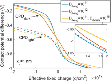
Lastly, the effects of the interface state density are explored. I begin by bringing the charge centroid closer to the interface,  nm, since this is typically the case for the intrinsic charge inside of dielectric thin films, as opposed to surface corona discharge. The interface state density at mid-gap (
 ) is first set to a value of 1011 cm−2eV−1 in accordance with figure 4. The CPD is then calculated both for dark and
  5 × 1018 cm−3s−1 as pictured in blue in figure 6. Increasing the mid-gap state density for acceptor and donor like states to 1012 cm−2eV−1 has a resulting CPD pictured in red, where it is clear that the CPD elongates along the
  axis. The SPV value also reduces in the whole range of charge analysed. Secondly, the mid-gap value is brought back to 1011 cm−2eV−1, and the value of interface states at both edges of the bandgap are increased to 1015 cm−2eV−1. This produces a reduction in the swing that CPD takes when going from accumulation to inversion. This is indicative of the higher concentration of charged stored in interface states rather than as free carrier at the silicon surface (
 and
and  ). The SPV value seems to be less affected for such lager band tails. Provided a KP instrument is capable of detecting differences in CPD in the order of 10's of mV, the interface physical changes modelled here would be evident and would allow the interpretation of different processing routines leading to changes to the interface.
Figure 6. CPD calculated for SV and SPV experiments on a Si-SiO2 interface with the charge centroid at 1 nm from the interface, and for different mid-gap interface state density conditions, while keeping the band tail states at the value shown in figure 4.
Download figure:
Standard image High-resolution image
5. Conclusions
This work reports a complete theoretical treatment of the surface voltage arising from the distribution of charge across a dielectric-semiconductor interface. This treatment allows analytical modelling of the results of Kelvin probe measurements, both in the dark and under illumination of an arbitrary light source, and including four key physical mechanisms: the charge stored in interface surface states, the charge stored in a dielectric thin film, the effects of changing effective lifetime and excess carrier densities, and the non-uniformity of charge. The proposed algorithm and solution in this work provide extremely valuable insight into the physics of dielectric-semiconductor interfaces, especially the influence of charge distributions. Such added understanding is critical in interpreting the results from KP SV and SPV measurements and using them as guide for the improvement of optoelectronic devices.
Acknowledgments
R.S. Bonilla is supported by the Royal Academy of Engineering under the Research Fellowship scheme. This work was supported by the UK Engineering and Physical Sciences Research Council grant number EP/V038605/1. For the purpose of Open Access, the author has applied a CC BY public copyright licence to any Author Accepted Manuscript (AAM) version arising from this submission.
Data availability statement
No new data were created or analysed in this study.
Supporting information
An open access Matlab script for calculation of all equations in this work is openly available on https://github.com/OxfordInterfacesLab.