
Abstract
Because of their excellent optical and electrical properties, Cu2ZnSnS4 (CZTS) thin films have been considered as a potential absorber layer for solar cells. However, CZTS suffers from some problems, such as secondary phases, antisite defects, and band tailing issues. Introducing Cd into CZTS to form Cu2CdxZn1−xSnS4 (CCZTS) is an effective method for alleviating the limitations of CZTS. In this study, the nanoparticle ink method was used to fabricate CCZTS thin films, and the effect of Cd content on the properties of CCZTS thin films was studied. The results showed that the as-prepared thin films had high purity, good crystallinity and photocurrent response. The photosensitivity and power conversion efficiency increased at first and then decreased with increasing Cd content. Due to the relatively excellent crystallization and photoresponse characteristics, the highest conversion efficiency of 0.72% was obtained when x = 0.3.
Export citation and abstract BibTeX RIS

Original content from this work may be used under the terms of the Creative Commons Attribution 4.0 licence. Any further distribution of this work must maintain attribution to the author(s) and the title of the work, journal citation and DOI.
1. Introduction
Cu2ZnSnS4 semiconductors have been considered as an ideal absorber layer for solar cells, because of their optimal band gap, nontoxicity and earth-abundant elements [1–4]. To date, the best active area efficiency based on CZTS was 13.6% [5]. However, the existence of Cu/Zn antisite defects, complex secondary phases, and band tailing restrict the development of CZTS-based solar cells [6–10].
To improve the photoelectric performance of the CZTS absorber layer, several chemical elements have been introduced, such as Ag, Na, Cd, Fe, and Co [11–15]. The Introduction of Cd into CZTS can yield multiple benefits. First of all, the band gap of CCZTS can be adjusted between 1.1 eV to 1.5 eV with different Cd content [16, 17]. Second, the addition of Cd can inhibit the formation of CuZn and ZnCu antisite defects [18]. Third, Cd in CCZTS can enlarge the single-phase region, consequently reducing the secondary phase [19]. There are different ways of Cd substitution. Su et al [20–22] adopted sol-gel method to prepare the precursor solution with Cd doped in advance and then thin films were prepared by spinning-coating method. By this method, the power conversion efficiency was successfully increased from 5.1% (bare Cu2ZnSnS4) to 12.6% (Cu2Cd0.4Zn0.6SnS4). Yan et al [23] deposited CdS layer on top of a cosputtered Cu/ZnS/SnS precursor. Then CCZTS thin films were prepared by interdiffusion at high temperature. As a result, a beyond 11% efficient CCZTS solar cell was achieved. In addition of these methods, nanoparticle ink method is also an excellent method to fabricate thin films. The largest advantage of this method is that the target phase can be formed in advance. At the same time, it also has the advantages of low-cost and eco-friendly. However, there is little precedent for preparing CCZTS thin films by nanoparticle ink method in the existing reports.
In this study, CCZTS thin films were prepared using the nanoparticle ink method. First, CCZTS nanoparticles were synthesized by the microwave irradiation method. The particles were then used to form the ink. Finally, CCZTS thin films were prepared by the spin coating method. The reagent used in the nanoparticle ink method has a low price and good volatility, and the amount of C impurities introduced in the preparation process is low.
2. Experimental
2.1. Materials
Copper (II) nitrate trihydrate (Cu(NO3)2·3H2O), zinc (II) acetate dihydrate (Zn(Ac)2·2H2O), cadmium (II) diacetate dihydrate (Cd(Ac)2·2H2O), stannous (II) chloride dihydrate (SnCl2·2H2O), thioacetamide (CH3CSNH2), n-propanol (C3H8O), triethanolamine (C6H15NO3) and polyvinylpyrrolidone (PVP) were purchased from Aladdin Reagent. Ethylene glycol (C2H6O2) was purchased from Sinopharm Reagent.
2.2. Synthesis of CCZTS nanoparticles
In a typical reaction, 0.036 M Cu(NO3)2·3H2O, 0.01 M Zn(Ac)2·2H2O, 0.01 M Cd(Ac)2·2H2O, 0.02 M SnCl2·2H2O, 0.24 M CH3CSNH2, and 0.64 g PVP were dissolved into a beaker with 50 ml ethylene glycol. After the precursors became clear and transparent, the solutions were placed in a microwave oven with a reaction power of 240 W for 10 min, and then allowed to cool to room temperature in air. The precipitates were separated from the solution by centrifugation at 8000 rpm for 8 min and washed several times with deionized water and ethanol. Then, the precipitates were dried under vacuum at 60 °C for 12 h to obtain the CCZTS nanoparticles. CCZTS nanoparticles (300 mg) were added to n-propanol (6 ml). Then, the nanoparticle ink was ultrasonicated for 2 h, and 0.75 ml triethanolamine was added to the ink. To obtain different kinds of ink, the precursor solution was prepared with different Cd/(Zn+Cd) ratios, and the Cd/(Zn+Cd) ratios were 0, 0.3, 0.5, 0.8, and 1.0.
2.3. Preparation of CCZTS thin films
The CCZTS nanoparticle ink was deposited on a molybdenum glass substrate by spin coating. The spin coating was repeated 30 times at 2500 rpm for 20 s, followed by preheating at 280 °C for 2 min on a hot plant in air. After that, the samples were sulfurized with a double zones tube furnace. The zone of S powder was set at 300 °C for 10 min with a heating rate of 5 °C min−1 while the zone of precursor samples was set at 600 °C for 10 min with a heating rate of 10 °C min−1. The air pressure was maintained at 300 mbar during annealing process.
2.4. Fabrication of CCZTS solar cells
The 50 nm thick CdS layer was deposited on sulfurized CCZTS via chemical bath deposition (CBD). ZnO with a thickness of 50 nm and ITO thickness of 300 nm were deposited by magnetron sputtering under an Ar atmosphere. Finally, the silver paste was printed on ITO and served as the top contact electrode.
2.5. Characterizations
The morphologies and elemental contents of the as-prepared CCZTS thin films were characterized using a scanning electron microscope (SEM, SU8010) equipped with an energy dispersive spectrometer (EDS). The phase and crystallographic information were obtained from x-ray diffraction (XRD, D8 Advance with Cu Kα radiation source) and Raman spectroscopy (InVia Reflex). The valence states of the CCZTS thin films were studied by x-ray photoelectron spectroscopy (XPS, PHI5702 with Al Kα irradiation). Transmission spectra were recorded in the wavelength range of 300–1100 nm using an Evolution 220. The photocurrent response spectra of the CCZTS films and current density-voltage (J-V) curves for solar cells were obtained using a 2450 SourceMeter under simulated 1 sun AM 1.5G illumination.
3. Results and discussion
Figure 1 showed the XRD patterns of CCZTS particles by microwave irradiation method. The peaks at 28.08°, 48.16° and 55.87° were corresponding to (112), (220) and (312) planes of kesterite CZTS (JCPDS No. 26–0575). However, the full width at half maxima (FWHM) of (112) peak was wide, which indicated worse crystallinity. Meanwhile, when x was larger than 0.5, some secondary phases appeared, such as CdS and CdyZn10-yS10. Moreover, with increasing Cd/(Zn+Cd), the intensity of peak attributed to CdS phase was enhanced.

Figure 1. The XRD patterns of Cu2CdxZn1−xSnS4 particles.(x = 0–1.0).
Download figure:
Standard image High-resolution imageThe XRD patterns of the annealed thin films are shown in figure 2. The crystallinity of all five samples was much better than that of the particles. The secondary phases also disappeared after sulfurization treatment, as shown in figure 2(a), which might be due to the reaction between the secondary phase CdS and the main phase CZTS during the sulfurization process to form the CCZTS phase. The diffraction peaks at 28.6°, 33.0°, 47.4°, 56.2°, and 59.0° were attributed to the (112), (200), (220), (312), and (224) planes of the CCZTS thin films. As shown in figures 2(b) and (c), it was found that the (112) and (220) planes indicated a slight deviation to the left with increasing Cd content. The peak shift could be attributed to lattice expansion caused by the substitution of Zn2+ (0.75 Å) by Cd2+ (0.80 Å) with a larger ionic radius [24]. A transition from kesterite Cu2ZnSnS4 to stannite Cu2CdSnS4 was observed when the ratio of Cd exceeded 0.5. This transformation has been previously reported [25].
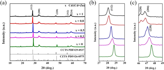
Figure 2. (a) The XRD patterns of annealed CCZTS films from 10 to 70°; (b) The partial enlarged patterns for (112) plane; (c) The partial enlarged patterns for (220) plane. (x = 0–1.0).
Download figure:
Standard image High-resolution imageRaman scattering was studied to obtain further information on these possibly coexisting secondary phases in the thin films (figure 3(a)). The obtained Raman spectra from the thin films showed only one peak at approximately 330 cm−1, corresponding to the characteristic peaks of CCZTS, which is generally denoted as the A1 vibration mode [26, 27]. Meanwhile, the peaks of the CCZTS thin films shifted from 331 to 325 cm−1 as the Cd content increased from 0 to 1.0. This was mainly due to the lattice expansion caused by the substitution of Zn by Cd, and the scattering frequency of the molecule to the incident light shifts towards the low-frequency region. Additionally, no secondary phases were identified in the Raman spectra. This result was similar to that of XRD.
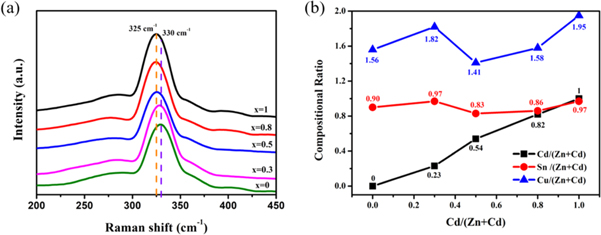
Figure 3. (a) Raman spectra of CCZTS thin films; (b) the ratio of M/(Zn+Cd) (M = Cu, Sn, Cd) of CCZTS. (x = 0–1.0).
Download figure:
Standard image High-resolution imageThe data measured by energy dispersive spectrometry (EDS) were processed and plotted as a broken line chart shown in figure 3(b). The Cd/(Zn+Cd) ratio of the samples was close to that of the precursor. The Sn/(Zn+Cd) line showed that the Sn content in the samples was lower than the (Zn+Cd) content. This was inferior to the dosage used in the preparation. This was possibly because a small amount of Sn in the sample escaped in the form of SnS at high temperatures during the sulfurization process. The values of Cu/(Zn+Cd) were all lower than 2, indicating that all the thin films were Cu-poor. As for the chemical composition of the absorber layer, it is commonly accepted that Cu-poor compositions are beneficial for high-efficiency solar cells.
X-ray photoelectron spectroscopy (XPS) was used to further study the valence states of CCZTS. Figures 4(a)–(f) show the XPS spectra of the as-prepared thin films. From the wide-scan XPS spectra (figure 4(a)), the peaks of Cu 2p, Cd 3d, Zn 2p, Sn 3d, and S 2p can be easily observed. A distinct impurity peak of C 1s was also observed. The incorporation of carbon mainly resulted from the incomplete volatilization of n-propanol and triethanolamine. Figure 4(b) shows the high-resolution Cu 2p spectra. Two peaks were fitted at the binding energy of 951.7 eV (2p1/2) and 931.8 eV (2p3/2). The distance between the two peaks was 19.9 eV, which corresponded to the expected binding energy of Cu+ [28]. The peaks of Cd 3d (figure 4(c)) at binging energy of 411.7 eV and 405.1 eV, with a peak splitting of 6.6 eV, were indicated of Cd2+ [29]. In figure 4(d), the Zn2+ state was confirmed by peaks sit at 1044.5 eV and 1021.4 eV with its characteristic peak separation of 23.1 eV [30]. From figure 4(e), it could be observed that two peaks located at 493.9 eV and 485.5 eV. The gap between Sn 3d3/2 and 3d5/2 was consistent with the binding energy of Sn4+ [20]. From the XPS results in figure 4(e), four weak shoulder peaks sat at 495.9 eV (x = 0–0.8), which was near the Sn 3d3/2 peak. These peaks could be attributed to the Zn-Auger peak L3M45M45 and became weak with an increase in the Cd/(Zn+Cd) ratio [31]. The sulfur spectra (figure 4(f)) could be assigned to the presence of S2− at binding energies of 162 eV and 163 eV with a doublet separation of 1.2 eV [32]. Overall, the XPS results were in line with the experimental expectations and were consistent with those of XRD.

Figure 4. XPS spectra of CCZTS: (a) wide-scan spectra, (b) Cu 2p, (c) Cd 3d, (d) Zn 2p, (e) Sn 3d, (f) S 2p. (x = 0–1.0).
Download figure:
Standard image High-resolution imageSEM images of the as-prepared thin films are presented in figure 5. The bare CZTS thin films had irregular microspheres and many large voids on the surface of the thin film. The average size was approximately 200 nm (figure 5(a)). By introducing a small amount of Cd (x = 0.3), the crystalline grains grew to reduce void structures, and the average size was approximately 400 nm (figure 5(b)). Thus, the surface of the thin film is denser. When the ratio of Cd/(Zn+Cd) was 0.5, the surface of the thin film consisted of grains with different shapes, and the sizes of the grains were smaller (figure 5(c)). It was inferred from XRD that this phenomenon was related to the crystal transformation. The coexistence of CCZTS with different crystal structures prevented the crystals from absorbing each other, causing hard growth during the sulfurization process, and the crystals were broken due to stresses. With a further increase in Cd, the crystalline grain became larger, and the size of the crystalline grain was approximately 300 nm (figure 5(d)). In addition, the bare CCTS thin film had micro-bricks on the surface, and the size of the sample was nearly 300 nm (figure 5(e)). Thus, introducing Cd to replace Zn at an appropriate ratio could help increase the crystalline grain size and improve the compactness of thin films.
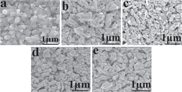
Figure 5. SEM images of CCZTS thin films: (a) x = 0; (b) x = 0.3; (c) x = 0.5; (d) x = 0.8; (e) x = 1.0.
Download figure:
Standard image High-resolution imageFigure 6 showed the transmittance spectra and band gap of the samples. From figure 6(a), it could be found that the average transmittances in the visible region (400 nm–800 nm) were all less than 10%, and along with the content of Cd elevating, the transmittances rose at first, and then decreased. When Cd/(Zn+Cd) surpassed 0.8, the transmittances of CCZTS thin films were near to 0. All the five samples showed an obvious absorption edge between 800–900 nm. The values of optical band gap were calculated by using formula (1) and (2). The results were demonstrated in figure 6(b). Following the increase of Cd content from 0 to 1.0, there was a trend of first decrease and then increase about the band gap, and the band gap was 1.46 eV, 1.30 eV, 1.31 eV, 1.36 eV and 1.37 eV, respectively. The possible reason of this nonlinear dependence was that the lattice expansion caused by Cd substitution, which lead to the decrease of the conduction-band minimum and relative band gap (up to x = 0.5). Moreover, the increase of band gap value while Cd contents higher than 0.5 may be caused by crystal transition [21].


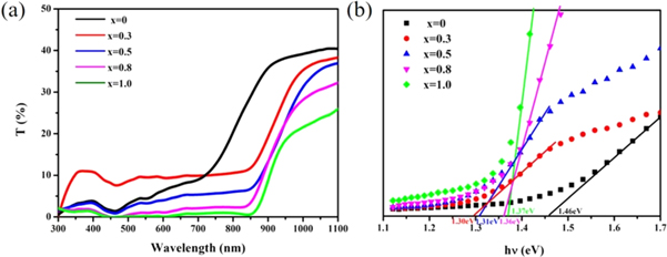
Figure 6. (a) The transmittance spectra of CCZTS thin films; (b) the band gap determined by (a).
Download figure:
Standard image High-resolution imageThe photosensitivity of the CCZTS thin films was detected using a photocurrent test (figure 7). During the test, the light and dark currents were measured by applying a bias voltage of 2 V. Among them, 0–15 s, 30–45 s, 60–75 s, 90–100 s were the currents under dark conditions, and the others were under illumination. When the thin films were in the dark, the current curves were very flat. The change in current was very clear when the samples were exposed to light. Meanwhile, during the three tests, the response of each sample did not indicate significant changes, which suggested that the CCZTS thin films had good stability.


Figure 7. Photocurrent response of CCZTS thin films: (a) x = 0; (b) x = 0.3; (c) x = 0.5; (d) x = 0.8; (e) x = 1.0.
Download figure:
Standard image High-resolution imageThe conductivity under the dark state (σD), conductivity under illumination (σL), and photosensitivity of CCZTS thin films were calculated using formula (3), as shown in table 1. The data under dark conditions was the value at 14 s, and the current under light was the value at 29 s. With the increase in Cd/(Zn+Cd), the photosensitivity of the as-prepared thin films strengthened at first (x = 0–0.3) and weakened later (x = 0.5–1.0). According to the results of XRD and SEM, numerous voids and grain boundaries in the bare CZTS thin films caused serious carrier recombination, which affected carrier transport. When the Cd/(Zn+Cd) ratio was 0.8 or 1.0, the structure of CCZTS had transformed from kesterite to stannite. Thus, the properties of the as-prepared thin films also changed accordingly. When the Cd/(Zn+Cd) ratio was 0.5, it was simultaneously affected by the above two aspects. The best photosensitivity of CCZTS was up to 2.18 with a substitution amount of 0.3.
Table 1. Summary of photocurrent test for CCZTS films with different Cd content.
| Dark electrical conductivity | Light electrical conductivity | Photosensitivity | |
|---|---|---|---|
| x | σD/(Ω−1·cm−1) | σL/(Ω−1·cm−1) | σL/σD |
| 0 | 7.24 × 10⁻⁴ | 14.4 × 10⁻⁴ | 1.99 |
| 0.3 | 2.72 × 10⁻⁴ | 5.94 × 10⁻⁴ | 2.18 |
| 0.5 | 7.38 × 10⁻⁴ | 14.3 × 10⁻⁴ | 1.93 |
| 0.8 | 0.42 × 10⁻⁴ | 0.79 × 10⁻⁴ | 1.88 |
| 1.0 | 0.11 × 10⁻⁴ | 0.18 × 10⁻⁴ | 1.63 |
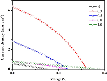
To further investigate the influence of Cd substitution on the performance of solar cells, photovoltaic studies on CCZTS thin films were carried out. Figure 8 showed the illuminated (AM 1.5) current-voltage (J-V) curves for CCZTS thin-film solar cells. Through these curves, we can read the open circuit voltage (VOC) and short circuit current (JSC) values of CCZTS solar cells. Then, the fill factor (FF) and power conversion efficiency (η) were calculated by formula (4), (5), (6).


Figure 8. J-V curves of CCZTS thin film solar cells.
Download figure:
Standard image High-resolution image
All the main parameters were showed in table 2. The main influencing factor of the devices was the quality of the heterojunction. From this table, VOC and JSC of the bare CZTS thin-film solar cell were lower than those of the CCZTS. This was related to the uneven surface of CZTS, which was not conducive to the growth of CdS and the large number of holes and grain boundaries in the CZTS thin films. When x was higher than 0.5, the value of the current density was smaller, which might be due to the higher resistance. One possible reason for this is the change in the crystal structure. The electrical properties of stannite are different from those of kesterite, and the lattice mismatch between CdS and the absorber layer (CdS/CCZTS) is serious [21]. The device exhibited the highest power conversion efficiency of 0.72% of Cd/(Zn+Cd) = 0.3, with VOC, JSC, and FF values of 323 mV, 6.43 mA·cm−2, 34.6%, respectively.
Table 2. Detailed parameters of CCZTS solar cells.
| Cd/(Zn+Cd) | η (%) | VOC (mV) | JSC (mA·cm−2) | FF (%) |
|---|---|---|---|---|
| 0 | 0.021 | 143 | 0.55 | 27.0 |
| 0.3 | 0.72 | 323 | 6.43 | 34.6 |
| 0.5 | 0.2 | 239 | 2.82 | 29 |
| 0.8 | 0.06 | 229 | 0.77 | 33 |
| 1.0 | 0.07 | 365 | 0.77 | 25 |
4. Conclusion
In this study, the nanoparticle ink method was used to prepare CCZTS thin films with different ratios of Cd/(Zn+Cd). The CCZTS thin films underwent a structural transformation from kesterite to stannite. With this transformation, the band gap of the thin films decreased at first (x = 0–0.3) and then increased (x = 0.5–1.0). In addition, introducing Cd to replace Zn could increase the grain size and improve the compactness of the thin films. Via the photocurrent test and current density-voltage (J-V), the photosensitivity and power conversion efficiency first increased and then decreased with increasing Cd content. The highest conversion efficiency of CCZTS solar cells was 0.72% and the photosensitivity was up to 2.18, when the Cd/(Zn+Cd) ratio was 0.3.
Acknowledgments
This work was financially supported by the National Natural Science Foundation of China (61804069, 51904128, 51802130).
Data availability statement
The data that support the findings of this study are available upon reasonable request from the authors.
Conflicts of interest
There are no conflicts of interest to declare.