
Abstract
Low-power, flexible, and properly encapsulated integrated circuits are the basic requirements of the solution-processed printed and wearable electronic prototypes for various emerging applications including display circuits, sensors, and radio-frequency identification tags. The organic field-effect transistor is one of the important types of devices used in such prototypes and its industrial applicability is essential for the printed electronics technology. The performance deterioration upon encapsulated through the thick layer of air-stable dielectric material such as amorphous fluoropolymer [CYTOP] - must be compensated by device engineering. In this work, we used furan and thiophene flanked diketopyrrolopyrrole donor-acceptor conjugated polymers namely PDPPF-DTT and PDPPT-DTT, and its comparative study was performed using Cytop as a dielectric material. The work advances interface engineering towards the single-gate and dual-gate organic transistors. Dual-gate transistors performance modulation using Cytop dielectric opens new research avenues towards stability enhancement of such transistors for real-world applications.
Export citation and abstract BibTeX RIS

Original content from this work may be used under the terms of the Creative Commons Attribution 4.0 licence. Any further distribution of this work must maintain attribution to the author(s) and the title of the work, journal citation and DOI.
1. Introduction
Organic Field-Effect Transistors (OFETs) with different active channel organic semiconducting materials have been demonstrated using bottom-gate (BG) [1–3], top-gate (TG) [2, 4, 5], and dual-gate (DG) configurations [6–21], respectively. Although, Bottom Gate Bottom Contact (BG-BC) has gained a special interest in sensing technology due to the ease of the exposure of the semiconductor material directly to the analyte [1]. However, in BG-BC configuration, the active channel organic semiconductor material has a high tendency to degrade due to interaction with the environmental conditions (e.g. moisture, oxygen) arising from the unprotected organic layer [22–25]. Due to strong hydrophobicity, and perfect solvent orthogonality with organic semiconductors. Asmall relative dielectric constant (κ, kappa) amorphous fluoropolymer such asCytop] has been widely used as low-k gate dielectrics for OFETs. Recently, our group successfully demonstrated that for better performance of the OFETs in BG-BC mode there is a need to encapsulate them with an environmentally stable dielectric material such as Cytop via surface passivation engineering [26].
It has been previously demonstrated that Cytop film has lower sensitivity of the dielectric strength on the underlying semiconductor film morphology and the low charge trapping [27]. Highly hydrophobic fluoropolymer, such as Cytop is more effective in removing the various environmental effects and it acts as a promising encapsulation layer. After Cytop encapsulation, OFET devices exhibit reduced hysteresis and also suppress the considerable penetration of moisture and other contaminants from the environment. Due to Cytop's use as interface encapsulation layer, the low band donor-acceptor (D-A) organic semiconductors like DPP-DTT can be protected for making stable transistor devices [28]. However, upon encapsulation with material such as Cytop, the device characteristics performance deteriorates to a certain extent [29] based on the thickness of the Cytop [27]. This must be investigated carefully for the considered polymer material and compensated through device engineering so that OFETs even after a proper performance can be retained to the best possible extent. In recent years, conjugated polymers based on electron efficient moiety diketopyrrolopyrrole (DPP) attracted great interest in organic electronics due to their applications in various electronic devices including transistors, solar cells, logic circuits, and sensors [22, 30, 31]. Due to their outstanding characteristics including low cost, easy synthesis and strong electron-withdrawing nature of DPP moiety, it has become an attractive building block to create functional materials for organic and printed electronics. Furthermore, DPP possesses strong light absorption, highly conjugated and coplanar structure, and good photochemical stabilities, making DPP-based polymers a promising choice of materials for OFETs [32–36]. In order to enhance the coplanarity and charge carrier mobility, dithieno[3,2-b:2',3'-d] thiophene (DTT) moiety has been used as electron-donating moiety for synthesizing D-A polymers. DTT is also well known for its strong intermolecular S···S interactions, structural planarity, and close intermolecular π–π stacking [37–39]. Further, Jung et al [40] and Sonar et al [33] have been reported D-A polymers based on thiophene-flanked DPP or furan-flanked DPP as an electron-deficient unit with DTT as an electron-rich unit for OFET and OPV applications in two different research works. Recently, using furan-flanked DPP material, we have shown that effective surface treatments, can improve the performance of the OFETs to a larger extent [41].
In this work, we present the device performance evaluation of both DPP–DTT polymers using the common Cytop interfacial dielectric layer at the ambient conditions, and the impacts of Cytop treatment studied in detail. Furthermore, we presented our dual-gate organic field-effect transistor (DG-OFET) which is capable of retaining and improving the original performance of the BG-BC OFET even under the presence of the 740 nm-thick Cytop layer. The study began with precisely optimizing the fabrication of thin films of Cytop directly on the PDPPT-DTT and PDPPF-DTT channel semiconducting thin films. Typically, in the DG-OFETs, the active semiconducting layer is isolated from the top and bottom electrodes by the presence of two gate insulators, thereby, forming two charge accumulation channels. In this work, we used silicon dioxide (SiO2) as one dielectric to isolate the bottom gate, and Cytop layer as another dielectric to isolate the top gate from the active organic semiconductor. Both SiO2 and Cytop have been widely used gate dielectric materials in the past. In order to understand the effect of a thick Cytop coating on BG-BC OFET, we used the DPP class of polymers namely PDPPF-DTT, and PDPPT-DTT (with furan and thiophene as flanking groups) as an active organic semiconductor material with bandgaps of 1.39, and 1.26 eV for comparative analysis. We observed that upon depositing Cytop dielectric, the device performance of the BG-BC OFETs degrades in terms of threshold voltage shifts to a substantive large value of −26.0, and −13.6 V from the earlier values of −2.21, and 0.02 V for PDPPF-DTT, and PDPPT-DTT in ambient conditions, respectively. To overcome such negative impact of the Cytop on the device power consumption and switching speed purpose, we implemented a DG-OFET device geometry and demonstrate that it is possible to retain almost the origin threshold voltage values with improved trap state density.
2. Experimental section
The OFET devices, in BG-BC, and Dual-Gate configurations were used to analyze the performance of PDPPF-DTT and PDPPT-DTT polymers [42]. During the OFET device fabrication, a p++ highly doped silicon substrate with SiO2 as the gate dielectric layer was used. The thickness of the SiO2 was 200 nm. These substrates were thoroughly cleaned by immersing them in Piranha solution, and further were heated at 80 °C for 10 min. The Piranha solution from the substrate was removed by rinsing them with deionized (DI) water for three times. Additionally, the substrates were ultra-sonicated with DI water first, toluene second, and isopropyl alcohol (IPA) third for 10 min each. Then, the substrates were baked at 100 °C for 1 h, exposed to ethanol vapor at 150 °C, and then the UV-Ozone (UV/O3) treatment for 10 min was done in that order. Metal for bottom contact as source and drain (S/D) was established by depositing a 70 nm thick gold (Au) using the thermal vacuum deposition chamber, herein the shadow mask had the channel length and channel width were 100 μm and 1.5 mm respectively. During electrical characteristic measurement and analysis, their actual deposited channel length and width exact values were measured via laser microscope imaging. Furthermore, to achieve a better work function for better charge carrier injection, the S/D electrode surfaces were modified by dipping them in a 30 mM solution of pentafluorobenzenethiol (PFBT) in isopropanol for 5 min and then rinsed properly with pure isopropanol. Both PDPPF-DTT and PDPPT-DTT polymers solutions were formed in chloroform using 7 mg ml−1 concentration and stirred using the magnetic stirrer at 300 rpm for 20 min. This solution was then spin-coated on the substrates at 1000 rpm for the 60 s and post-annealed at 150 °C for 30 min in the nitrogen (N2) environment, and then the thickness was determined. This is the reference device and it is showed as figure 1(e)-(Reference). Another set of dual-gate devices were fabricated inside the Nitrogen environment following the same procedure using Cytop (CTL-809M) as dielectric layer deposition. To reduce the thickness of the Cytop, we mixed it with its solvent named CT-SOLV180. Both the Cytop and its solvent were procured from the company AGC-Chemicals. Through spin coating, the Cytop layer was optimized for an average thickness of 740 nm on top of the semiconductor layer. Then the measurement was performed at ambient condition for device type figure 1(e)- (Device-1). All the fabricated devices were characterized using a standard Keithley semiconductor parameter analyzer (5 channels, Keithley, 4200A-SCS) at ambient conditions. The same devices were then used for figure 1(e)- (Device-2). measurements at ambient conditions, after depositing 70 nm-thick Au as the top gate via thermal vacuum deposition. In the case of output characteristics (ID–VDS), drain-voltage (VDS) sweep from 0 to −40 V, and drain-current (ID) were measured. Similarly, for transfer characteristics (ID–∣VGS∣), gate-voltage (VGS) sweeps from 10 to −40 V.
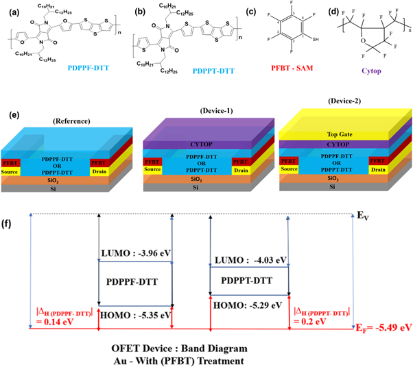
Figure 1. The molecular structures of (a) PDPPF-DTT, (b) PDPPT-DTT, (c) PFBT, (d) Cytop, (e) Device structures of OFETs studied; (Reference) is a reference device tested in air, (Device-1) is a device type under the presence of the Cytop as encapsulation, and (Device-2) is a device type with a top gate over the Cytop for dual gate operation and (f) Describes OFETs band diagram with PFBT treated Au as the source-drain electrode.
Download figure:
Standard image High-resolution image3. Results and discussion
Figures 1(a) and (b) show molecular structures of PDPPF-DTT and PDPPT-DTT polymers respectively. Figure 1(c) shows the molecular structures of PFBT used as SAMs for S/D contact treatment. Figure 1(d) shows the molecular structures of Cytop act as dielectric material, as well as the encapsulation layer for environmental stability. The experiments were systematically devised for comparative analysis purposes to understand the OFET device performance of PDPPF-DTT and PDPPT-DTT polymer semiconductors upon using Cytop and in the presence of dual gates.
Firstly, as in figure 1(e) - (Reference), the performance of both these polymers at the ambient conditions was determined. Secondly, as in figure 1(e)- (Device-1). the performance of bottom gate bottom contact was analyzed in presence of the Cytop. Thirdly, as in figure 1(e)- (Device-2) represents dual-gate OFET devices. The dual-gate configuration was implemented by depositing top electrode over the Cytop, and the measurements were done by applying the step-by-step voltage on the top gate bias while doing the full sweep of the bottom gate. This figure 1(e) - (Device-2) configuration also has been utilized during, only top gate bottom contact sweeps, and during the dual-gate sweep mode; wherein, a simultaneous sweep where applied at both the top and bottom gates.
Figure 1(f) describes the band diagram of both these polymers used in OFETs under the presence of the PFBT treated Au electrode with the work function increased from −4.76 eV to—5.49 eV. In the case of PDPPF-DTT, the LUMO level is −3.96 eV, and HOMO level of −5.35 eV; thereby, the barrier height(∆H) in this material is estimated around ∣0.14∣ eV. Whereas, in the case of PDPPT-DTT, the LUMO level is −4.03 eV, and HOMO level of −5.29 eV; leading to the barrier height(∆H) in this material to be ∣0.20∣ eV. Au S/D metal work function changes were determined by Photo-Electron Spectroscopy in Air (PESA) technique using Riken AC-3 equipment, and the result is shown in figure S7.
3.1. OFET performance evaluation of PDPPF-DTT and PDPPT-DTT
We studied PDPPF-DTT and PDPPT-DTT as active channel semiconducting materials and SiO2 (200 nm thick) as a gate dielectric over p++-Si substrate which acts as a gate electrode. The comparison between the two devices is shown in figure 2 in terms of their device geometry and transfer characteristics. The central focus of this study is to investigate the dielectric-semiconductor interface through threshold voltage (VTh) measurement, and the interface trap density calculations in their hysteresis counterpart.
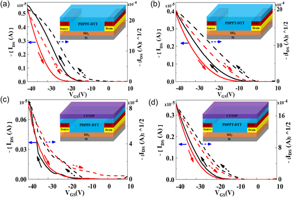
Figure 2. OFETs transfer characteristics comparison of (a), (c) PDPPF-DTT, (b), (d) PDPPT-DTT; in ambient condition and in presence of Cytop (c), (d) without any top-gate bias, respectively; (black line: forward; red line: reverse).
Download figure:
Standard image High-resolution imageParameters obtained from standard analysis for all OFET devices are summarized in table 1. Mobility and sub-threshold swing (SS) are calculated from equations (S1) and (S2) (available online at stacks.iop.org/MRX/8/096301/mmedia) respectively, while VTh is calculated from √ID versus VGS plot by extrapolating the plot to ID = 0, at VDS = −40 V, in the saturation region. From table 1, we observed that PDPPF-DTT material has always higher mobility than and PDPPT-DTT. To validate this, as shown in figure S6, we compared the thin film AFM morphology of these polymers on the SiO2 surface. We observed that the average nominal height of 3.47 nm was measured in the case of PDPPF-DTT which is smaller than 3.68 nm in the case of PDPPT-DTT polymer thin film. This decreased roughness leads better stacking in the case of PDPPF-DTT leading to better mobility. We achieved mobility of 0.098 cm2/Vs for PDPPF-DTT, and 0.031 cm2/Vs for PDPPT-DTT at VDS = −40 V for reference devices shown in figures 2(a) and (b), respectively. Also, figure 2(a) has a larger hysteresis than figure 2(b). Such hysteresis effects in OFET devices are studied by various research groups for charge carrier trapping and their density calculations [43, 44]. We obtained the change in VTh in two cycles of the hysteresis curve and calculated the trap density ( ) in each case by using the following equation [45]:

Where  is dielectric capacitance, and
  is the electronic charge. We obtained the trap density for PDPPF-DTT and PDPPT-DTT based OFET devices are 8.3 × 10¹¹ and 2.1 × 1011 cm−2, respectively. Large trap density in PDPPF-DTT based OFETs may be distributed in the organic layer and around the dielectric-semiconductor interface and the metal-semiconductor interface, which gets suppressed by adding a Cytop encapsulating layer on top of it. In PDPPF-DTT material, trap density decreases from 8.3 × 10¹¹ to 3.8 × 1011 cm−2 after the deposition of the Cytop layer. Similarly, in PDPPT-DTT material, trap density decreases from 2.1 × 10¹¹ to 1.3 × 1011 cm−2 after Cytop deposition, which is clearly seen by reduced hysteresis in figures 2(c) and (d), respectively. The source of these electron traps might be oxygen (O2
−) and hydroxyl ions (OH−) which are reduced by Cytop encapsulating layer [46–49]. Again, smaller sub-threshold swing (SS) and trap density in PDPPT-DTT based OFET devices confirm that the formation of a good dielectric-semiconductor interface in this material. PDPPF-DTT and PDPPT-DTT based OFET devices give SS values 1.99 and 1.48 V/dec for reference devices shown in figures 2(a) and (b), respectively. After Cytop deposition, SS values also decrease from 1.99 to 1.6 V/dec for PDPPF-DTT based OFET devices, and for PDPPT-DTT devices these values decrease from 1.48 to 1.33 V/dec. This decrease in SS values also confirms the improved performance of devices after the reduction of oxygen (O2
−) and hydroxyl ions (OH−) due to top Cytop encapsulating layer deposition. These are negatively charged electron traps at the dielectric-semiconductor interface due to oxygen (O2
−) and hydroxyl ions (OH−) which enhances the gate-field and starts the accumulation of charge carriers at the smaller VTh. Larger electron traps reduce the VTh value [50].
is the electronic charge. We obtained the trap density for PDPPF-DTT and PDPPT-DTT based OFET devices are 8.3 × 10¹¹ and 2.1 × 1011 cm−2, respectively. Large trap density in PDPPF-DTT based OFETs may be distributed in the organic layer and around the dielectric-semiconductor interface and the metal-semiconductor interface, which gets suppressed by adding a Cytop encapsulating layer on top of it. In PDPPF-DTT material, trap density decreases from 8.3 × 10¹¹ to 3.8 × 1011 cm−2 after the deposition of the Cytop layer. Similarly, in PDPPT-DTT material, trap density decreases from 2.1 × 10¹¹ to 1.3 × 1011 cm−2 after Cytop deposition, which is clearly seen by reduced hysteresis in figures 2(c) and (d), respectively. The source of these electron traps might be oxygen (O2
−) and hydroxyl ions (OH−) which are reduced by Cytop encapsulating layer [46–49]. Again, smaller sub-threshold swing (SS) and trap density in PDPPT-DTT based OFET devices confirm that the formation of a good dielectric-semiconductor interface in this material. PDPPF-DTT and PDPPT-DTT based OFET devices give SS values 1.99 and 1.48 V/dec for reference devices shown in figures 2(a) and (b), respectively. After Cytop deposition, SS values also decrease from 1.99 to 1.6 V/dec for PDPPF-DTT based OFET devices, and for PDPPT-DTT devices these values decrease from 1.48 to 1.33 V/dec. This decrease in SS values also confirms the improved performance of devices after the reduction of oxygen (O2
−) and hydroxyl ions (OH−) due to top Cytop encapsulating layer deposition. These are negatively charged electron traps at the dielectric-semiconductor interface due to oxygen (O2
−) and hydroxyl ions (OH−) which enhances the gate-field and starts the accumulation of charge carriers at the smaller VTh. Larger electron traps reduce the VTh value [50].
Table 1. Obtained parameters for both PDPPF-DTT, and PDPPT-DTT OFET devices.
| Device types figure 1. (e) | Organic semiconductor | Vth(F)(V) | Vth(R)(V) | ∣Vth (Diff)∣(V) | (μFET)(cm2/V s) | (SS)(V/dec) | Ntrap (/cm2) |
|---|---|---|---|---|---|---|---|
| Reference | PDPPF-DTT | −2.21 | −10.1 | 7.89 | 0.09 | 1.48 | 8.3 × 10¹¹ |
| Reference | PDPPT-DTT | 0.02 | −2.03 | 2.05 | 0.03 | 1.99 | 2.1 × 10¹¹ |
| Device-1 | PDPPF-DTT | −26 | −22.3 | 3.7 | 0.01 | 1.6 | 3.8 × 10¹¹ |
| Device-1 | PDPPT-DTT | −13.6 | −14.8 | 1.2 | 0.05 | 1.33 | 1.26 × 10¹¹ |
| Device-2 | PDPPF-DTT | −2.8 | −5.28 | 2.48 | 0.06 | 3.66 | 3.2 × 10¹¹ |
| Device-2 | PDPPT-DTT | −2.03 | −2.29 | 0.26 | 0.03 | 0.84 | 3.4 × 10¹⁰ |
From table 1, it is clear that after Cytop deposition, trap density decreases in both the cases which confirms the reduction of oxygen (O2 −) and hydroxyl ions (OH−) at the bottom dielectric-semiconductor interface. In this manuscript, we did not characterize the top dielectric-semiconductor interface. After Cytop deposition, a slight variation in mobility might be due to a change in morphology at the top dielectric-semiconductor interface. Figure 3 illustrates the effect of fixing the top gate bias with −30 V and the full sweep dual-gate behavior for PDPPF-DTT and PDPPT-DTT based OFET devices using SiO2 (200 nm-thick) and Cytop (740 nm-thick) as bottom, and top gate dielectric materials, respectively. Figures S1 and S3 showcase the transfer characteristics of PDPPF- DTT and PDPPT-DTT OFET transfer characteristics in dual-gate mode with step-by-step top gate sweeps. Figures S2, and S4 showcase output characteristics of the PDPPF-DTT, and PDPPT-DTT OFETs with of device types figure 1(e)-(Reference), (Device-1), and (Device-2), respectively. Further, device type figure 1(e)-(Device-2), figure S5 compares the transfer characteristics of only top gate bottom contact bias characteristics for PDPPF-DTT, and PDPPT-DTT OFETs, and table S3 summarize their results of electrical performances.

Figure 3. OFETs comparison of transfer characteristics at VDS = −40 V, (a), (c) PDPPF-DTT, (b), (d) PDPPT-DTT; in top gate fixed bias of −30 V, and in the dual-gate bottom and top gate full sweep mode, respectively; (black line: forward; red line: reverse).
Download figure:
Standard image High-resolution image3.2. Threshold voltage and trap density variation under different configurations
When we compare device 1 and device 2 in table 1, we observed that the mobility value increases after dual-gate operation at fixed top gate at VGS = −30 V from −0.015 to 0.066 cm2/Vs in PDPPF-DTT based OFETs while in PDPPT-DTT based OFETs, mobility decreases from 0.057 to 0.0343 cm2/Vs in dual-gate operation. To calculate the mobility for dual-gate OFET, we used the net capacitance as a parallel combination of the top (Cytop gate dielectric) and bottom (SiO2 gate dielectric) capacitors (Ctop + Cbottom = 4.0 + 16.8 = 20.8 nF/cm2). Formation of the second channel on the top-gate side helps to increase drain current and hence mobility [51]. Figures 4(a) and (b) show the observed results of the variation of forwarding bias VTh and NTrap with respect to various devices configurations understudy and corresponding values are reported in table 1.

Figure 4. (a) Variation of the forward bias VTh, (b) showcases the variation of the NTrap, w.r.t OFET device types (Reference, Device-1, and Device-2) respectively.
Download figure:
Standard image High-resolution image
Further, for figure 1(e)-(Device-2), table S1 and S2 summarize the results of electrical performances of PDPPF-DTT and PDPPT-DTT OFETs, with step-wise voltage increase in top-gate bias, respectively. Electron traps form a sheet of negative charges at the dielectric-semiconductor interface and enhance the gate field which in turn reduce the VTh values in OFET devices. Lower trap density (1.3 × 1011 cm−2) in device type 1 in figure 4(a) contributes less in gate field gives higher VTh values compared to the other two devices [50]. Thereby, we demonstrate that upon operating the Cytop encapsulated DPP polymer-based OFET in dual-gate mode the low-powered operation with reduced VTh, and traps is possible.
Although the interface trap density is suppressed with Cytop deposition for bottom gate OFETs (table 1), the small decrease in mobility in the case of PDPPT-DTT dual-gate OFETs might be due to the quality of the top dielectric-semiconductor interface formation. Drain-current transients for both the top-and bottom-gate OFETs give information about the quality of the interface formed [45].
4. Conclusions
In summary, we studied single and dual-gate OFET based on furan and thiophene - flanked DPP namely, PDPPF-DTT and PDPPT-DTT polymers as active channel semiconductors. We have clearly demonstrated that the performance deterioration in terms of threshold voltage upon encapsulation through the thick layer of air-stable Cytop can be compensated by device engineering through dual-gate mode operations. The dielectric-semiconductor interface has been investigated in terms of the shift in VTh due to hysteresis in transfer characteristics, and trap density calculations. PDPPF-DTT material has always higher mobility than and PDPPT-DTT. Smaller sub-threshold swing (SS) and trap density in PDPPT-DTT based OFET devices, in comparison to PDPPF-DTT material, confirm the formation of a good dielectric-semiconductor interface in SiO2 and PDPPT-DTT. Deposition of cytop layer on top sidehelps to reduce the oxygen (O2 −) and hydroxyl ions (OH−) trap concentration. Dual-gate OFET illustrates high current, and mobility in comparison to single gate OFET because of the formation of a second channel on the top gate side. Hence, this work provides important progress by enhancing the device performance even after encapsulation with the thick Cytop layer.
Acknowledgments
B B Patil and T T Do, A S are thankful to QUT for offering scholarships to conduct the research work. We are thankful to CRC for Polymers, Central Analytical Research Facility (CARF), and Institute of Future Environments, Queensland University of Technology (QUT) for providing equipment support. P Sonar is thankful to QUT for the financial support from the Australian Research Council (ARC) for the Future Fellowship (FT130101337) and QUT core funding (QUT/322120-0301/07). A K Pandey acknowledges funding from AISRF (Project 53820).
Data availability statement
All data that support the findings of this study are included within the article (and any supplementary files).
Authors contribution statement
B B Patil, Y Takeda, S Tokito, Samarendra P, Ajay K Pandey, Prashant Sonar designed the collaborative research. B B Patil, Y Takeda performed the device fabrication and related experimental work. Kostya Ostrikov provided suggestions while writing the manuscript. B B Patil, Subhash Singh, Amandeep Singh performed the data analysis, and wrote the manuscript, incorporating the comments from all the authors. Thu Trang Do, Prashant Sonar provided the polymer, and description of the material. All authors have given approval to the final version of the manuscript.
Competing interests
The authors declare no competing interests.