

Abstract
The deposition of niobium film on copper with excellent superconducting property at low-temperature conditions, used as superconducting radio frequency (SRF) cavity, is a serious and urgent technical problem to be solved at present. In this work, copper-based niobium (Nb) films with a thickness of 1.5–1.8 um, regulating the deposition temperature parameters and gas flow velocity in a tube furnace, were prepared by low-temperature chemical vapor depositing (CVD) method from the reaction between H2 and Niobium chloride (NbCl5) under pure Ar atmosphere. Fabricated Nb films were characterized by X-ray diffraction, scanning electron microscopy and energy dispersive spectroscopy, respectively. The results showed that the excellent crystalline quality and superconductive performance of Nb films were generated successfully by CVD at low temperatures of 650 °C–700 °C. The preparation process was optimized during deposition and the formation mechanism of Nb films was also discussed in detail. The magnetic moment versus temperature of the Nb sample prepared at 700 °C was also measured and the well-prepared Nb film deposited in the boundary layer region obtains the desired superconducting transition temperature of 9.1 K ± 0.1 K, almost equivalent to that of high pure Nb bulk material. The optimized CVD reaction method of Nb film with favorable morphology and expected superconductive property at low temperature provided a new strategy and technical process in designing the desired copper-based Nb film SRF cavity.
Export citation and abstract BibTeX RIS

Original content from this work may be used under the terms of the Creative Commons Attribution 4.0 licence. Any further distribution of this work must maintain attribution to the author(s) and the title of the work, journal citation and DOI.
1. Introduction
The superconducting radio frequency (SRF) cavity based on niobium (Nb) material is adopted by the particle accelerator due to its unique superconductivity [1, 2]. Although the heat transfer efficiency can be increased by utilizing a thin-walled SRF cavity [3], however, its performance and lifetime would be susceptible to structural deformation caused by mechanical vibration and helium pressure disturbance. To reach satisfied thermal conductivity using high-purity Nb bulk material, its excessive-high manufacturing cost also restricts the development of accelerator [4, 5]. Benefiting from the high thermal conductivity of copper and the low penetration depth (<1 μm) of the RF field attenuation to 1/e of the cavity surface [2, 6], the structure of Nb film on the inner wall of the thick-walled copper cavity can achieve consistent superconducting performance in contrast to that of pure Nb. In addition, the thermal and mechanical stability of the SRF system would be also enhanced remarkably [7, 8].
A lot of work on the preparation of niobium films by physical vapor deposition (PVD) were reported in CERN, Jlab, and LBNL laboratories [9, 10], but the deposition rate was relatively low and it was not suitable to deposit a uniform film on complex substrate surface [11]. Reduction-reaction of Niobium chloride (NbCl5) with H2 by chemical vapor deposition (CVD) could provide a feasible solution to resolve the problems mentioned above. Jun. Z et al. concluded that the increasing temperature of the collection zone and excessive hydrogen was beneficial to obtain high-purity Nb powder, but it was easy to form a solid mixture composed of Nb and H impurity when reaction temperature reached 1000 °C [12, 13]. Liu. Q et al studied the morphology of the Nb film layer deposited on the SiC substrate in the temperature range of 850 °C–1300 °C. They concluded that increasing deposition temperature was conducive to the formation of large-size grains. Meanwhile, the Nb film can react with SiC substrate as the temperature was higher than 1150 °C, causing the deterioration of superconductivity of Nb film [14, 15]. The deposition temperature of Nb films prepared by CVD was mostly between 850 °C–1300 °C in reported papers, thus the copper substrates were prone to thermal deformation, which will increase the stress of the films and the deposition quality of the film is seriously affected. The excellent superconducting transition performance for copper-based Nb film based on the low-temperature CVD process (<850 °C) has not been fully examined so far. The thermodynamics reaction and kinetics of surface diffusion or adhesion capacity of precursor composition are susceptible to reaction temperature in the CVD process. The gas flow velocity at high temperature also plays a vital role in the crystallization quality and superconducting property of the Nb film [16]. Reasonable regulation of reaction temperature and gas flow velocity is necessary to optimize deposition process parameters in the CVD process. However, up to now, the effects of gas flow velocity on the preparation of superconductive Nb film under low-temperature conditions (especially < 800 ℃) is very limited. Thin films deposited in the stratosphere and the boundary layer have not been compared, and the reasons for the difference in film quality in different regions have not been studied. To the best of our knowledge, only one paper was reported by Pizzol. P et al. [2], which successfully prepared the Nb film on the copper substrate with excellent superconductivity utilizing CVD below 800 °C. Whereas limited to its complicated and costly chamber design, the preparation efficience and practicability of Nb film might be deficient.
Therefore, in the present study, a facile tubular furnace process was employed to fabricate Nb films through CVD on copper substrates using a hydrogen reduction route at low temperatures. The dependence of crystal structure, surface morphology, and element component Nb film on the reaction temperature and gas flow velocity was investigated systematically. In addition, the superconducting property of Nb films was tested.
2. Experimental details
The oxygen-free copper substrates with a size of 1. 5 cm × 1. 5 cm × 1.0 cm were mechanically polished with sandpaper before deposition. After that, the substrate was ultrasonically cleaned in alcohol and acetone for 10 min for 3 cycles. Then it was rinsed with deionized water to remove the alcohol and finally dried for later use. The schematic diagram of the CVD experimental setup is illustrated in figure 1. The NbCl5 (purity of 99. 9%), as the precursor, was placed inside the non-constant temperature zone of the quartz tube. To maintain continuous NbCl5 vapor flow and prevent vapor condensation, the heating wire heats NbCl5 to sublimation temperature to provide a steady reaction stream of NbCl5. The deposition kinetics process of CVD can be influenced by the deposition temperature and precursor flow rate according to the boundary layer theory [17] and Grove model [18]. The gas flow velocity plays an important factor to affect the precursor steam flow rate and surface reaction [19]. Due to the middle position of the advection zone is the position where the gas velocity is the maximum, and the boundary area is the minimum [17], So one of the substrates was fixed at the center of the stratosphere, labeled as substrate 1, the other one was placed at boundary layer (the tube wall), labeled as substrate 2, as shown in figure 1 concretely.
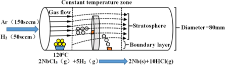
Figure 1. Schematic diagram of the experimental setup, showing the growth conditions for the growth of the Nb films.
Download figure:
Standard image High-resolution imageThe carrier gas Ar (purity of 99. 99%) passed through the ceramic crucible with a flow rate of 150 sccm and Ar carried NbCl5 vapor into the deposition chamber. H2 was supplied as reducing gas into the deposition chamber at a flow rate of 50 sccm. The deposition temperatures were varied from 550 °C to 700 °C. The Nb film deposition lasts one hour, then the as-grown samples were naturally cooled to room temperature. Because of the strong corrosion of chlorine and hydrogen chloride, the pipe joints were equipped with copper plug nets and a vacuum dust filter was installed at the front of the mechanical pump to reduce corrosion to the vacuum system.
X-ray Diffraction (XRD, Bruker D8 Advanced) with a Cu Kα radiation wavelength of 0.15418 nm was carried out to characterize the phase structure for the as-deposited Nb films, the XRD data was recorded at a scanning range of 30°–100° with a step of 0.01° and a dwell time of 4 s for each step. The evolution of crystalline sizes with the deposition temperature also was analyzed from XRD patterns. The surface micro-morphology, crystalline quality, and elemental composition of the as-deposited Nb films were characterized by the Scanning Electron Microscope (SEM, Inspect F50) equipped with Energy Dispersive Spectroscopy (EDS), respectively. A vibrating sample magnetometer (PPMS-9) tester was performed to measure the superconducting transition temperature (Tc) of the Nb films.
3. Results
3.1. Phase characterization of Nb films
Figures 2 and 3 showed the XRD patterns as a function of deposition temperature for the samples deposited at the center of the stratosphere area and boundary area (corresponding to the positions of substrate 1 and substrate 2 in figure 1). Additional XRD peaks resulting from the Cu substrate were found in all measured XRD patterns due to the x-ray beam penetration depth was higher than the film thickness. Basically, the diffraction peaks of copper substrates gradually became weaker with the temperature increasing from 550 °C to 700 °C, indicating that the thickness of the Nb film was gradually enhanced. The niobium oxide was formed in the Nb films prepared at 550 °C, the peak of niobium oxide decreased gradually as the temperature increased. At the same time, more characteristic diffraction peaks of Nb films including Nb (200), Nb (211), Nb (220), Nb (310) peaks appeared, and Nb (110) peak gradually became sharper and more intensive, suggesting that the Nb films on copper substrates were successfully synthesized by regulating the deposition temperature parameters.
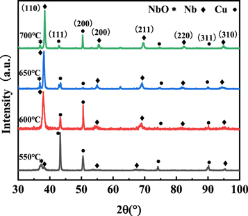
Figure 2. XRD patterns of Nb films on substrate 1 at different temperatures.
Download figure:
Standard image High-resolution image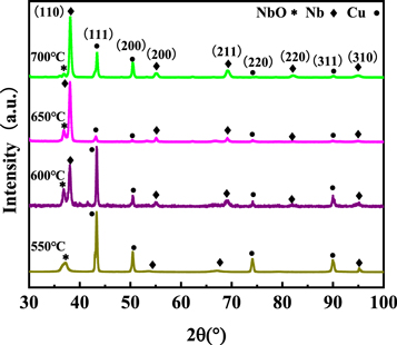
Figure 3. XRD patterns of Nb films on substrate 2 at different temperatures.
Download figure:
Standard image High-resolution imageAs it is known to all, the difference of crystal surface energy results in the deposition rate of the Nb film at each crystal plane direction, and the nucleation ability of the crystalline is various during the film growth process. From the crystallographic perspective, the Nb atoms are easily attracted by those crystal planes with higher surface energy, resulting in the growth space of the crystal nucleus is restricted and the crystal plane growth is shrunken gradually. However, the (110) crystal plane is the most densely packed plane with the lowest surface energy and slowest growth rate. As a result, the crystal nucleus grown on the (110) crystal plane can fully grow up before connecting other crystal nuclei, so they all show preferential growth orientation along the (110) crystal plane.
The structure parameters of Nb films deposited at substrate 1 and substrate 2 were shown in tables 1 and 2, respectively. On the one hand, the calculated lattice parameters of the as-deposited films were nearly identical to the pure Nb bulk materials (3.303 Å) when the temperature reached 600 °C–700 °C. The crystalline size of Nb films prepared at 550 °C was lower than other films, indicating that the formation of nano-crystallines was caused by a large number of grain boundaries [20]. The high-density grain boundaries and oxide impurity in Nb film degraded the superconducting properties and the Tc value would decrease significantly [21]. On the other hand, the Nb films at substrate 2 had higher crystallinity quality compared with those at substrate 1 due to the difference in the concentration of reactants, the thickness of the boundary layer, and the diffusivity of active species according to boundary layer theory [22]. The formation mechanism of Nb films will be further explained in the following discussion part.
Table 1. Structural parameters obtained from x-ray measurements of the Nb films at substrate 1.
| Temperature (°C) | FWHM | Lattice constant (Å) | Crystallite (nm) |
|---|---|---|---|
| 550 | 1.478 | 3.43 | 5.67 |
| 600 | 0.659 | 3.36 | 12.75 |
| 650 | 0.418 | 3.34 | 20.10 |
| 700 | 0.413 | 3.33 | 20.35 |
Table 2. Structural parameters obtained from x-ray measurements of the Nb films at substrate 2.
| Temperature (°C) | FWHM | Lattice constant (Å) | Crystallite (nm) |
|---|---|---|---|
| 550 | 1.183 | 3.43 | 7.08 |
| 600 | 0.424 | 3.35 | 19.82 |
| 650 | 0.398 | 3.34 | 21.11 |
| 700 | 0.296 | 3.32 | 28.41 |
3.2. Morphological characterization of Nb films
All of the as-deposited Nb films had a shiny silvery surface. The effects of temperature on the surface morphology of films deposited at different gas flow velocities were shown in figures 4 and 5. For the sample at substrate 1, the surface micro-graphs of Nb films presented discontinuity and non-uniformity (550 °C) structure, hilly structure occurred accompanied by ravines and valleys at the temperature of 600 °C. And a large number of holes could be observed when the temperature further increased to 650 °C and 700 °C, respectively. Abundant bulky particles were also accumulated on the surface of Nb film deposited at 700 °C. Because of the low reaction rate, substrate 1 formed discontinuous films at 550 °C. The various micro-topographies under 600 °C–700 °C were caused by the corrosion of Ar, H2, and the generated reactant intermedium, such as HCl, Cl, Cl2 [23]. Besides, deposition temperature and the flow rate of precursor NbCl5 also affected the uniformity of film topography [24]. In contrast, the Nb films at the substrate 2 showed a small number of ravines and micro-void as the deposited temperature increased from 550 °C to 600 °C, uniform surface and fewer hilly structures or holes defects were observed for the Nb film at temperature further increased to 650 °C–700 °C. Figures 6(a) and (b) showed the stratosphere and boundary layer samples at 700 ℃ respectively. According to the observation of the SEM cross-section, there is no obvious dividing line between niobium and copper, so we combined EDS linear mapping analysis, the thickness of the coatings produced at stratosphere and boundary layer was about 1.895 μm and 1.515 μm. Compared to substrate 1, the lower reactant vapor flow rate and higher product concentration profiles were dramatically conducive to the crystalline quality and flat surface according to the boundary layer theory [25] and Grove model [22], which would be discussed later.

Figure 4. Surface morphology of Nb films at different temperatures (Samples at the substrate 1, (a)–(d) series of reaction temperature at 550 °C; 600 °C; 650 °C; 700 °C).
Download figure:
Standard image High-resolution image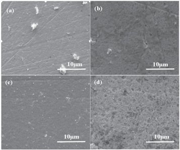
Figure 5. Surface morphology of Nb films at different temperatures (Samples at the substrate 2, (a)–(d) series of reaction temperature at 550 °C; 600 °C; 650 °C; 700 °C).
Download figure:
Standard image High-resolution image
Figure 6. Cross-section and elemental composition measured by EDS mapping and SEM. (a) stratosphere sample at 700 °C; (b) boundary layer sample at 700 °C.
Download figure:
Standard image High-resolution imageTo further observe the high-magnification microstructure, figure 7 showed the enlarged SEM micro-graphics of the samples deposited at substrate 2 under the temperature conditions of 650 °C and 700 °C. The structure of the Nb film (deposition temperature at 650 °C) consisting of randomly oriented fine-grained poly-crystals grew into dense and coherent irregular columnar crystalline, and then grew into larger columnar crystalline at the higher temperature (deposition temperature at 700 °C). The slight difference of the pin-hole structures on the sample surface was noticed in comparison with the sample deposited at 650 °C, these random pin-hole defects were formed by the fine-grained rapid aggregation into columnar crystalline, then lifting unfilled pinhole defects in the film.
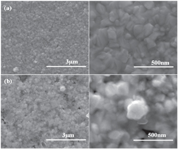
Figure 7. High magnification (a)–(b) SEM images of as-grown at 650 °C and 700 °C (Samples at the substrate 2).
Download figure:
Standard image High-resolution imageTo further characterize the variation of uniformity of film morphology, the 3D morphology and roughness of the Nb films deposited at 550 °C–700 °C were obtained by the optical profiler, as shown in figures 8–10. On the one hand, for the film deposited at substrate 1, the Sa (mean roughness) reduced from 90 nm to 43 nm and the Sq (root mean square roughness) decreased from 980 nm to 50 nm with the enhancement of deposition temperature due to the disappearance of hilly structures which were formed by ravines and valleys, as shown in figure 4. Combined with the 3D morphology of the niobium film surface, it can be seen that this is because the flatness and uniformity of the niobium film continue to improve with the increase of temperature. Furthermore, it was worth noting that the roughness and uniformity of the film deposited at substrate 1 were more easily affected by the temperature change, which should be attributed to gas flow velocity. Whereas the Sa reduced from 31 nm to 23 nm, and the Sq decreased from 37 nm to 31 nm with the increase of deposition temperature for the samples at the substrate 2. Combined with the three-dimensional surface morphology of the Nb film, the overall flatness and uniformity are higher than that of the substrate 1. The deposited Nb film showed smoother and more uniform, meaning that Nb films behaved better formation quality with the temperature rising. The roughness of the sample at substrate 2 was lower than the sample at substrate 1 due to the slower flow rate of precursor NbCl5. These results were consistent with the surface morphology observed from SEM images in figure 5.
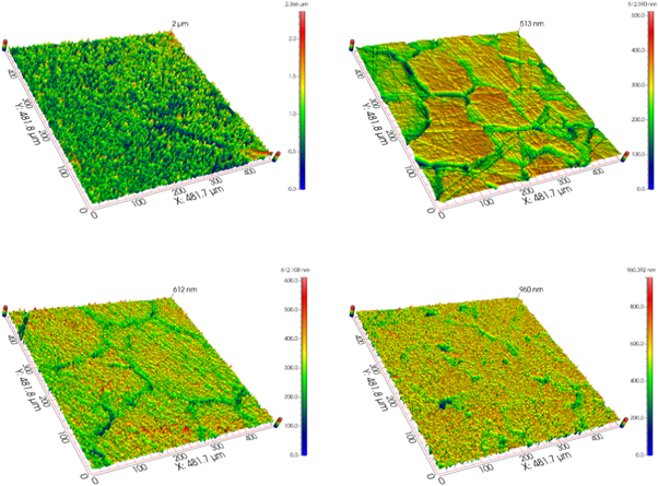
Figure 8. 3D morphology of Nb films at different temperatures (Samples at the substrate 1, (a)–(d) series of reaction temperature at 550 °C; 600 °C; 650 °C; 700 °C).
Download figure:
Standard image High-resolution image
Figure 9. 3D morphology of Nb films at different temperatures (Samples at the substrate 2, (a)–(d) series of reaction temperature at 550 °C; 600 °C; 650 °C; 700 °C).
Download figure:
Standard image High-resolution image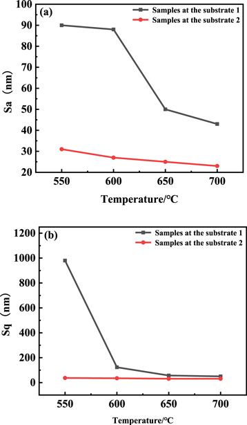
Figure 10. (a) Mean roughness of samples with different reaction temperatures at substrate 1 and substrate 2; (b) Root mean square roughness of samples with different reaction temperatures at substrate 1 and substrate 2.
Download figure:
Standard image High-resolution image3.3. Element component characterization of Nb film
Figures 11(a) and (b) showed the component content of Nb films prepared at different reaction temperatures of 550 °C–700 °C. The EDS results showed that the film contains certain pollutants, such as undetectable C and O elements, which produced an adverse effect on superconductivity properties [26]. For the sample deposited at substrate 1, the component of Nb increased linearly from 15.67% to 79.18% as the temperature increased from 550 °C to 700 °C. The component of Nb increased linearly from 15.67% (550 °C) to 52.99% (700 °C) for the sample deposited at substrate 2. It was concluded that the film thickness and the deposition rate were enhanced due to the temperature effect, which was consistent with the Arrhenius law [14, 27].

Figure 11. The component of elements in Nb films at different temperatures (a) Samples at the substrate 1; (b) Samples at the substrate 2.
Download figure:
Standard image High-resolution image3.4. Analysis of superconducting transition temperature
The crystal structures and the morphology were characterized thoroughly for the Nb films prepared at different deposition temperatures and gas velocities, it was found out that the Nb film deposited at 650 °C–700 °C of boundary layer area displayed higher crystalline quality and smoother surface morphology. The superconducting transition temperature of the sample deposited at 650 °C could not be measured due to the Nb film without enough thickness, Therefore, samples from two deposition zones at 700 °C were selected to detect the superconducting transition temperature. As illustrated in figure 12(a), Samples were divided into two parts to test the temperature dependence of magnetic moment, by which the superconducting transition temperature of the sample was also measured.
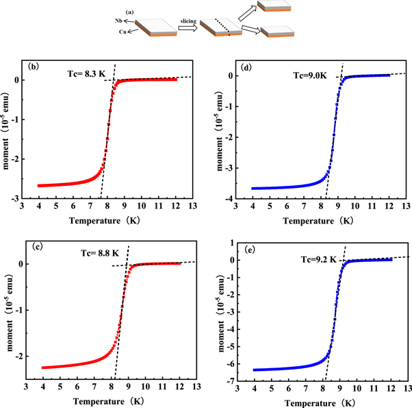
Figure 12. (a) Schematic diagram of the grown niobium film sample cut in half; (b)–(c) Temperature dependence of magnetic moment of stratosphere Nb films; (d)–(e) Temperature dependence of magnetic moment of boundary layer Nb films.
Download figure:
Standard image High-resolution imageFigures 12(b) and (c) showed the temperature dependence of the magnetic moment of the Nb film of the stratosphere area. The magnetic moment of the Nb film was 7.6 × 10⁻⁸ emu at 10 K. As the tested temperature of the Nb film decreased, the magnetic moment began to drop sharply at 8.3 K and then reached −2.01 × 10⁻⁵ emu at 7.8 K. It could be regarded as that the superconducting transition temperature of the Nb film was 8.3 K. At the same time, the temperature dependence of the magnetic moment of the Nb film of sample 2 as shown in figure 12(c). The magnetic moment of the Nb film was −1.72 × 10⁻⁸ emu at 10 K, the magnetic moment reduced sharply at 8.8K and then dropped sharply at 8.3 K to −1.60 × 10⁻⁵ emu. It could be concluded that the superconducting transition temperature of the Nb film was 8.8 K. Figures 12(d) and (e) showed the temperature dependence of the magnetic moment of the Nb film of boundary layer area. The magnetic moment of the Nb film was −1.8676 × 10⁻⁷ emu at 10 K. As the tested temperature of the Nb film decreased, the magnetic moment began to drop sharply at 9.0 K and then reached −3.11542 × 10⁻⁵ emu at 8.4 K. It could be regarded as that the superconducting transition temperature of the Nb film was 9.0 K. At the same time, the temperature dependence of the magnetic moment of the Nb film of sample 2 as shown in figure 12(e). The magnetic moment of the Nb film was −3.79174 × 10⁻⁷ emu at 10 K, the magnetic moment reduced sharply at 9.2 K and then dropped sharply at 8.4 K to −5.26157 × 10⁻⁵ emu. It could be concluded that the superconducting transition temperature of the Nb film was 9.2 K. Compared with the stratosphere samples, the boundary samples show better superconducting properties. The Tc value (9.1 K ± 0.1 K) of the film was almost consistent with that of the pure Nb bulk materials (9.3 K) [28]. The sample in the stratosphere has lower crystallinity and a large number of defects on the surface compared with the sample in the boundary layer area since the crystallinity and defects play important roles in affecting superconducting transition temperature [20]. Therefore, the optimized Nb film deposited at 700 °C in the boundary layer area displayed outstanding superconducting transition temperature.
4. Discussion
For the determination of Nb film deposition kinetics in the CVD process, basic fluid mechanics concepts could be applied to CVD to describe the fluid dynamics and mass transfer in the gas phase. The fluid flow in a CVD process could be characterized by several dimensionless parameters such as the Reynolds number (Re) and Knudsen number (Kn) as follows:


where ρ = mass density, u = flow density, μ = viscosity, and where λ is the mean free path and L is the characteristic length. Re defines the limit between the laminar and turbulent (Re > 2100) flow regimes whereas, Kn defines the limits between laminar, intermediate, and molecular flow [29, 30]. Most CVD reactors operate in the laminar regime (Re < 100) due to the low precursor flow rate. The rate of mass transport is dependent on the concentration of reactants and the thickness of the boundary layer. The thickness of the boundary layer δ defined as:


The thickness of boundary layer δ is related to the Reynold number Re, and the flow rate u presents gradient distribution in the region of the boundary layer [22]. The schematic diagram of the H2 and NbCl5 flow process can be illustrated in figure 13, the NbCl5 precursor flow rate was fast at substrate 1 according to the flow rate distribution characteristic, leading to the reductive NbCl5 precursors were deposited rapidly accompanied by the vapor flow. The nucleation and crystallization growth of Nb film at substrate 1 was influenced by the fast vapor flow. As a result, the Nb film with disadvantageous crystalline quality and uneven morphology was obtained at substrate 1 in comparison with the film deposited at substrate 2. Because of the maximum value of Re, the flow rate was minimum at substrate 2 according to equation (4) [18]. NbCl5 precursors almost reacted with hydrogen fully, the sample located at substrate 2 exhibited a slower deposition rate, displaying better crystalline and superconducting property compared with the sample at substrate 1.
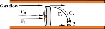
Figure 13. The schematic diagram of the H2 and NbCl5 flow process.
Download figure:
Standard image High-resolution imageThe reaction process of NbCl5 can be illustrated in figure 14, which can be divided into two parts. The first part is the reaction between chloride adsorbed on the target and hydrogen. Insufficient reactive intermediate species results in low surface mobility of adsorbed Nb atoms, the deposition occurs essentially at the sites where adsorption occurred. The second part is the reaction in the atmosphere of NbCl5 and hydrogen generating niobium steam. Part of the Nb vapor is deposited on the substrate.

Figure 14. Schematic of Nb deposition process.
Download figure:
Standard image High-resolution image
The reaction between adsorbed NbCl5 and H2 could be influenced by temperature changes a lot. At lower temperatures (lower than 650 °C), chlorine substances were adsorbed (Cl(ad)), occupying some active sites on the growth surface and reducing the number of potential reactive sites of the precursor molecule NbCl5 [31, 32]. The niobium chloride decomposition rate was reduced and there existing discontinuous film on the surface of the substrate was observed in SEM. The fast reaction flow should be responsible for a rougher film containing a large number of defects. At higher temperatures of 650 °C–700 °C, the adsorbed Nb-containing species could therefore find a particular orientation with the lowest interfacial free energy for nucleation, and the increased surface mobility resulted in deposited film at substrate 2 with better crystallinity and fewer defects, which was consistent with sharper Nb (110) peaks in XRD patterns.
5. Conclusion
Superconductive Nb films on copper substrates, regulating the deposition temperature parameters and gas flow velocity, were prepared by low-temperature chemical vapor deposition (CVD) method from the reaction between H2 and NbCl5 under pure Ar atmosphere. The effects of reaction temperature (550 ℃–700 ℃) and the gas flow velocity on the crystal structure, morphology, and element component of the Nb films were investigated, and eventually, according to the crystal quality of the film, the superconducting transition temperature of the samples in two areas with deposition temperature of 700 ℃ was measured. The Nb films with higher crystallinity quality and fewer defects were generated successfully by CVD at substrate 2 compared with those prepared at substrate 1 due to the difference of concentration of reactants. Compared with the superconducting transition temperature of the Nb film prepared at the stratosphere, the expected superconducting transition temperature (9.1 K ± 0.1 K) for the Nb film prepared at boundary layer area with a low depositing temperature of 700 °C, which was almost the same as pure Nb bulk material (9.3 K) due to the corresponding microstructure with high crystallinity quality and fewer defects. The optimized CVD reaction parameters of Nb film with favorable microstructure and expected superconductive property at low-temperature conditions provided a new strategy and technical process in designing copper-based Nb film SRF cavity.
Acknowledgments
This work was supported by Sichuan Science and Technology program (No. 2020YFSY0007), Program National Natural Science Foundation (No. 11705252), Key research project of the Chinese Academy of Sciences (No. QYZDY-SSW-JSC019) and Scientific instrument development project of the Chinese Academy of Sciences (No. E028861Y). The author Kun Zhang is grateful to the Fundamental Research Funds for the central Universities for its financial supports.
Data availability statement
The data that support the findings of this study are available upon reasonable request from the authors.
Conflicts of interest
The authors declare no conflict of interest.