
Abstract
In this work lead sulfide nanoparticles are grown by simple chemical methods. The morphology of the materials is characterized by using x-ray diffraction, transmission, and scanning electron microscopy. The bandgap energy of materials is determined from near-infrared absorption spectra. The PbS films are deposited on indium tin oxide coated glass by the solution dip process. Photovoltaic devices are fabricated by depositing evaporated aluminum dots on PbS film. I-V characterizations of fabricated devices are performed under dark and illumination conditions. A comparative solar cell characteristic study is done among different nanomaterials based photovoltaic devices. The effect of particle size on the solar cell characteristics is studied.
Export citation and abstract BibTeX RIS

Original content from this work may be used under the terms of the Creative Commons Attribution 4.0 licence. Any further distribution of this work must maintain attribution to the author(s) and the title of the work, journal citation and DOI.
1. Introduction
The solar cell can produce direct current from solar energy. This renewable and eco-friendly energy can fulfill our increasing energy demands of a huge population in poor and backward Jangalmahal in India. PbS nanomaterials are emerging for their low-temperature solution processability [1, 2] for photovoltaic applications [3–5]. PbS nanoparticles are better applicable than PbSe, PbTe in telecommunications [6–9]. PbS nanostructures have electronic transitions in the near-infrared region [10–14]. The colloidal quantum dots have seen a rapid increase of interest in the last decade in optoelectronics due to their low cost, spectral tunability, and solution processing at room temperature [15–20]. The semiconducting nanoparticles (NPs) are considered a promising candidate in photovoltaics and photodetector also at a short- wavelength infrared [21–27]. PbS nanoparticles are a potential candidate for optical switching applications due to the third-order nonlinear optical response is 30 times than gallium arsenide (GaAs) and 1000 times than cadmium sulfide (CdS) [28]. PbS nanoparticles having a large value of mobility and dielectric constant are an interesting class of material for solar energy transfer due to the generation of multiple excitons [10]. Yoon et al [29] reported enhanced open-circuit voltage of metal–PbS Schottky by reducing non-radiative recombination processes. They found the value of VOC is 0.602 V, JSC is 6.7mA cm−2, FF value is 45.8%, and PCE value is 2%. Cheraghizade et al [30] deposited PbS thin films by CVD technique and studied the effect of anionic and cationic dopants' electrical and optical properties for photovoltaic application. They found the value of VOC is 0.52 V, JSC is 1.93mA cm−2, FF value is 29%, and PCE value is 5.02%. Speirs et al [31] performed solar cells comprising a layer of tetrabutylammonium iodide capped PbS and a layer of ethane dithiol capped PbS. An explanation is given according to the important electronic properties of PbS films. They found the value of VOC is 0.61 V, JSC is 25.8 mA cm−2, FF value is 60%, and PCE value is 9.4%. The present study is an attempt to compare the efficiency of PbS-Al Schottky solar cells by using three different shaped PbS nanomaterials.
2. Experimental
2.1. Material growth
PbS nanoparticles were grown from PbCl2, sulfur powder (S), and Sodium Borohydride. Sulfur is reduced by NaBH4.Ethylenediamine is used as a capping agent. Firstly at room temperature (25 °C) 60 ml, Ethylenediamine was poured into three beakers Next 2.78 g PbCl2 was dissolved into each beaker containing EDA and stirred for 30 min. Then 0.32 g of sulfur powder is added to these beakers. Finally, 0.37 g, 1.11 g, and 1.85 g NaBH4 are added in three beakers respectively. The stirring is continued for 4 h. Grown PbS are centrifuged, dried, and collected. The NaBH4 addition is corresponding to a 1:1:1 ratio of ingredients and leads to the formation of spherical shaped nanoparticles. The addition of 1.11 gm NaBH4 corresponds to a 1:1:3 ratio and leads to cubic shaped nanoparticles. Whereas 1.85 gm NaBH4 corresponds to a 1:1:5 ratio and leads to chain-like PbS nanoparticles.
2.2. Sample characterization
For structural determination, x-ray diffraction (XRD) of powder samples was carried out with High-resolution Rigaku Mini Flex x-ray Diffractometer. Transmission electron microscope (TEM) images PbS samples are obtained using JEOL-JEM 2100 HRTEM. Also, morphology was studied by powder samples in a JEOL-JSM 5800 Scanning Electron Microscope. Agilent Technologies Cary 5000 Series UV–vis-NIR Spectrophotometer is used to obtain absorption spectra for bandgap determination.
2.3. Device fabrication and characterization
The ITO-coated glass slide was thoroughly cleaned with detergent, De-ionised water, isopropanol, and acetone using an ultrasonicator. A small amount of PbS nano sample was added in ethanol kept in a beaker. The sample is dispersed by ultrasonication at room temperature. The cleaned ITO coated glass is partially dipped into the as-prepared dispersion so that PbS film deposits on the back conducting side. For making a Schottky barrier, aluminum is thermally evaporated and deposited on PbS film by the shadow mask. The size of the aluminum dot is 0.04 cm2. The schematic diagram of the fabricated device is shown in figure 1.
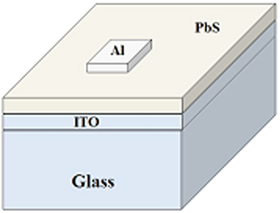
Figure 1. Schematic diagram of the fabricated device.
Download figure:
Standard image High-resolution imageThe current density measurement is performed with a semiconductor parameter analyzer Agilent 4155. I-V measurement is performed under dark and 1.5 AM solar irradiation.
3. Results and discussion
The XRD patterns of the grown sample are shown in figure 2. XRD pattern is obtained with Cu-Kα x-rays of wavelength 1.5418 A0. Diffraction peaks are indexed and correspond to the face-centered cubic phase of PbS (PDF card number 04-003-2980). The lattice constant (a = b = c) calculated from XRD data is 5.9 A0. Nanocrystal size can be estimated using the Debye–Scherrer relation [32] which is given by  where D is crystallite diameter, k is an average shape constant value of 0.94, λ is the x-ray wavelength (1.5405 Å), b is the full width at half-maximum (FWHM) value of the x-ray diffraction line, and 2θ is the diffraction angle in radians. This FWHM value is obtained using OriginPro 8.5 software. The size of the particles in the TEM pictures was measured using electron microscopy techniques. The particle size of spherical PbS nanoparticle is 8 nm while for cubic PbS nanoparticle is 13 nm, and for chain-like PbS it is estimated to be 19 nm.
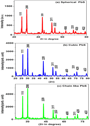
Figure 2. The XRD pattern of grown PbS samples.
Download figure:
Standard image High-resolution imageTEM images of synthesized samples are shown in figure 3.

Figure 3. TEM images of grown three different shaped PbS materials (a) Spherical PbS (b) Cubical PbS (c) Chain like PbS.
Download figure:
Standard image High-resolution imageThe nanoparticles are well distinct whereas the shape of the nanomaterial is different. The average sizes of spherical and cubic shaped particles are 8 nm and 13 nm respectively. The size of the chain-like PbS is about 19 nm.
SEM images of grown samples are shown in figure 4.

Figure 4. SEM images of grown different shaped PbS materials (a) Spherical PbS (b) Cubical PbS (c) Chain like PbS.
Download figure:
Standard image High-resolution imageThus different shaped, sized nanoparticles can be grown by varying the reducing agent to nanocrystal. With the increase of reducing agent ratio, the shape is changed from spherical to cubic and finally to the chain-like structure.
The different shapes are also observed in the SEM picture for samples grown with the increase of reducing agent ratios [26].
The NIR absorption spectra and bandgap of prepared samples are shown in figure 5.

Figure 5. (a) NIR absorption spectra, (b) bandgap determination of grown PbS nanoparticles.
Download figure:
Standard image High-resolution imageThe absorption spectra of different PbS samples of equal concentration are obtained by loading the dispersion in a cuvette after dispersed in an ethanol medium. The absorption edge of samples shifts towards a lower wavelength as particle size decreases.
Optical Absorption Coefficient (ɑ) is determined from absorption data at different wavelengths i.e. at different photon energy hѵ. To determine the bandgap  versus
  a plot is traced for each sample according to Tauc's relation. The plots are shown in figure 5(b). The linear portion of the graph is extrapolated to zero and the bandgap energy is derived from the intersection with the energy axis. Spherical and rectangular-shaped nanoparticles have bandgap energy 1.02 eV, 0.95 eV respectively, while the bandgap of the chain-like PbS is found to be 0.89 eV. The size of the chain-like PbS is larger than spherical as well as rectangular shaped nanoparticles. The bandgap energy of PbS nanoparticles is decreased due to the formation of large particles from the sintering and merger of smaller particles [33].
Current-voltage (J-V) characteristics of fabricated Schottky barrier PbS- Al solar cells with different sized PbS nanomaterials are displayed in figure 6.
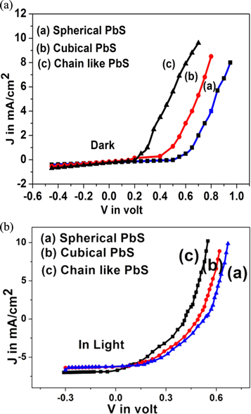
Figure 6. Current density versus Voltage characteristics of fabricated photovoltaic devices based on three different shapes PbS nanoparticles (a) in dark and (b) under light illumination.
Download figure:
Standard image High-resolution imageJ-V measurements are performed in dark and light conditions. The work function of spherical, cubical, and chain-like p-type PbS nanoparticles is referred as 5.1 eV, 5.25 eV and 5.28 eV respectively [14, 33, 34]. The work function of Aluminium (Al) is about 4.2 eV. The work function of Al is less than the work function of p-PbS nanomaterials. Since φm < φs (p-type), Al/p-PbS will form a Schottky barrier instead of an ohmic contact. This is evident from I-V characteristics. Hence the built-in potential is given by  where Eg, χs are the energy bandgap, electron affinity of semiconducting PbS nanoparticles and φm is the work function of metal (Al). From the calculation, we derived the built-in potential for the Schottky barrier as 0.9 V, 1.05 V, and 1.08 V of chain-like PbS, cubic PbS, and spherical PbS respectively. The reverse saturation current is small for the Schottky diode due to contribution only from minority carriers of the semiconductor side. Also, the reverse saturation current is of the order of nano ampere as there are no minority carriers on the metal (Al) side. The minority carriers contribution is only from the semiconductor i.e. PbS nanomaterials side. The reverse saturation current increases with the increase of crystallite size. This is probably due to the decrease of the recombination centers which are present at the metal-semiconductor interface [27]. PV device made by spherical shaped nanoparticle gives an open circuit voltage 0.53 V. Here, the surface of nanomaterials may be well passivated by using ethylenediamine. The highest efficiency is obtained by 1.41% for spherical shaped nanomaterials. PV device made by chain-like PbS gives Voc 0.41 Volt and efficiency 0.94%. The observed solar cell parameters, short circuit current density (Jsc), Fill factor (FF), efficiency, and sample characteristics are given in table 1. Efficiency is large for spherical particles. This shape has a larger surface area compared to other shapes. Also, the increase of bandgap for the spherical-shaped particle is due to a higher absorption at a lower wavelength of the solar spectrum [20]. The ideality factor of Schottky junction based on different shaped PbS nanoparticles in dark and under light is determined by the slope of semi-log forward bias ln (I) versus V graph using this relation given below.

Table 1. Characteristics and solar cell performance of different shape PbS nanoparticles.
| Sample (Shape) | Jmax in mA cm−2 | Vmax in Volt | JSC in mA cm−2 | J0 × 10−3 in mA cm−2 | Voc (V) | FF (%) | PCE (%) | Ideality factor in dark | Ideality factor in light |
|---|---|---|---|---|---|---|---|---|---|
| Spherical | 4.9 | 0.31 | 6.1 | 1.7 | 0.53 | 44 | 1.41 | 4.8 | 2.5 |
| Rectangular | 4.7 | 0.26 | 6.4 | 6 | 0.49 | 38 | 1.26 | 5.4 | 2.6 |
| Chain like | 4.3 | 0.22 | 6.8 | 24 | 0.41 | 35 | 0.94 | 5.8 | 2.8 |
The lnI versus V plot of fabricated photovoltaic devices based on three different shaped PbS nanoparticles in dark and under light illumination is shown in figure 7.

Figure 7. The lnI versus V plot of fabricated photovoltaic devices based on three different shapes PbS nanoparticles (a) in dark and (b) under light illumination.
Download figure:
Standard image High-resolution imageThe larger value in the ideality factor is observed in three Schottky devices. This can be explained by surface states [34]. Semiconductor surface i.e. PbS contains surface states due to unterminated covalent bonds which can lead to change at the metal-semiconductor interface. Also, PbS nanoparticles have a large surface area and hence involve surface states. The Schottky barrier junction includes termination of the semiconductor crystals and this can leads to changes at the metal-semiconductor interface. Hence the injected carriers will recombine due to the presence of surface states. Because of the surface state interfacial layer, the barrier height will have deviated from the predicted ideal value. As a result diode ideality factor deviates [35, 36].
Power density and Voltage characteristics of fabricated photovoltaic devices based on three different shaped PbS nanoparticles are shown in figure 8.

Figure 8. Power density and Voltage characteristics of fabricated photovoltaic devices based on three different shapes PbS nanoparticles.
Download figure:
Standard image High-resolution imageSolar cell performance of different shaped PbS nanoparticles is compared in table 1.
From current-voltage characteristics, we plot cut-in voltage (VOC), dark saturation current (J0), and the short circuit current density (JSC) as a function of bandgap energy of PbS nanoparticles and is shown in figure 9.
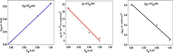
Figure 9. Variation of Voc, J0, and JSC with Eg of fabricated photovoltaic devices based on three different shapes PbS nanoparticles.
Download figure:
Standard image High-resolution imageThe non-linear current measured from an Al-(p)PbS Schottky contact is explained by the thermionic emission theory. According to this theory, the current density in the Schottky barrier [35] is given by
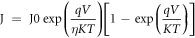
where Jo is the saturation current density, k is the Boltzmann constant, η is the ideality factor, T is the absolute temperature, q is the electron charge and V is the applied voltage.
The saturation current density Jo is written as
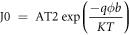
where A is the effective Richardson constant and ϕb is the barrier height. The ideality factor (η) and the saturation current density (Jo) of a Schottky diode are calculated from the slope of the linear region of the forward bias and the straight-line intercept.
The cut-in voltage (VOC) [37] is determined by the fundamental recombination process, and the direct measure of recombination in the device is considered as dark saturation current (J0) in mA cm−2. The cut- in voltage (VOC) [26] is given by putting J = 0 and considering JSC ≫ J0
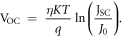
where JSC is the short circuit current density in mA cm−2 and η is the ideality factor.
The forward dark current density increases with an increase in the size of PbS nanoparticles. The Schottky barrier arises when the work function of the metal is less than the work function of semiconductors which is p-type.
The built-in potential value (Vbi) for different Schottky junctions showed the same trend as Voc with a large amount of band bending for smaller PbS nanoparticles. This large band-banding may lead to an increase in the hole-injection barrier and the enhancement of open-circuit voltage and fill-factor. This result is consistent with a decrease in the forward dark current density for smaller PbS nanoparticle devices, indicating that undesirable hole-injection to the aluminum metal electrode can be significantly reduced with the increase of the Schottky barrier height [38].
Comparing the increase in forwarding current among differently shaped particles the barrier height between Al and p-PbS increases for smaller PbS nanoparticles.
The Schottky junction is formed with aluminum metal contact, oxidation of Al also responds to a decrease in the built-in potential as indicated by a decrease in open-circuit voltage and series resistance. Again decrease in device performance may be due to decreased short circuit current by oxidation of PbS nanoparticles [35].
The dark saturation current (J0) is given by a function of bandgap energy (Eg) [39],  where J00 is a prefactor that depends on the current transport mechanism of the Schottky device [40].
The band diagram of the Schottky barrier junction made by growing three different shaped PbS materials and Al metal is shown in figure 10.

Figure 10. Band diagram of Schottky barrier junction made of grown three different shaped PbS materials and Al metal. (a)–(c) before contact and (d)–(f) after the formation of contact.
Download figure:
Standard image High-resolution image
The solar cell parameters, short circuit current density (Jsc), Fill factor (FF), efficiency, and sample characteristics are compared with previous work in table 2.
Table 2. Comparison of characteristics and solar cells' performance with previous work.
| Schottky | VOC (Volt) | JSC (mA cm−2) | FF (%) | PCE (%) | Year | References |
|---|---|---|---|---|---|---|
| Direct PbS deposited | 0.51 | 9.2 | 35 | 2.1 | 2013 | [41] |
| PbS (60 min spin coating) | 0.407 | 7.66 | 52.9 | 1.65 | 2014 | [42] |
| PbS QDs | 0.52 | 13.56 | 58 | 4.1 | 2017 | [43] |
| PbS nanocrystals | 0.51 | 10.92 | 30.7 | 1.71 | 2019 | [44] |
| PbS nanocrystals | 0.56 | 11.2 | 55 | 3.48 | 2019 | [45] |
| PbS nanoparticles | 0.53 | 6.1 | 44 | 1.41 | This work |
4. Conclusions
Three different shape PbS nanoparticles are grown by chemical methods. Structural characterization reveals that spherical, cubic, and chain-like PbS nanoparticles are grown using different reducing agent ratio. Optical absorption indicates that spherical nanoparticles have a higher bandgap and hence show quantum confinement effect as compared to chain-like PbS. The efficiency of photovoltaic devices grown from spherical nanoparticles show the highest efficiency and efficiency decreases as the particle size of used PbS material increases.
Acknowledgments
The authors are grateful to UGC & DST for their constant support through the SAP and FIST program to the Department of Physics, Vidyasagar University.
Data availability statement
The data generated and/or analysed during the current study are not publicly available for legal/ethical reasons but are available from the corresponding author on reasonable request.