
Abstract
Surface photovoltage (SPV) in p+-GaAs/p-GaAlAs/p-GaAs has been studied by establishing a multilayer model and measuring the SPV at room temperature. The model mainly considers surface recombination velocity, interface recombination velocity and the space charge region (SCR) at the surface of p+-GaAs. The SPV of the multilayer structure is shown to originate predominantly from the minority carrier diffusion, which caused photovoltage between the surface and bottom. Subsequently, the minority carrier diffusion lengths in p+-GaAs and in p-GaAs are obtained from fitting experimental data to the theoretical model. At the same time, the minority carrier diffusion length in p-GaAs is obtained by illuminating the backside (illuminating on p-GaAs) of the p+-GaAs/p-GaAlAs/p-GaAs. The p+-GaAs in p+-GaAs/p-GaAlAs/p-GaAs structure with different thickness are measured to show the variation of SPS with different thickness, but the experimental parameters are not affected. In multi-layer structure, the SPV contributed by different layers has a great difference with different dark saturation current density.
Export citation and abstract BibTeX RIS

Original content from this work may be used under the terms of the Creative Commons Attribution 4.0 licence. Any further distribution of this work must maintain attribution to the author(s) and the title of the work, journal citation and DOI.
1. Introduction
Gallium arsenic (GaAs) and its alloy materials are widely used in optoelectronics devices, power devices and high performance integrated circuits due to their physical characteristics of high temperature resistance, high electron mobility, electrons with small effective mass, et al [1, 2]. Because of the influence of minority carrier recombination and minority carrier diffusion on the performance of solar cell, for photocathode and other device which are based on GaAs materials, it's essential to study the minority carrier diffusion length and lifetime of GaAs materials in order to improve the device performance [3, 4].
Surface photovoltage spectrum (SPS) which is the curve of surface photovoltage (SPV) with incident photon energy has been used for the study of the minority carriers diffusion length, optical properties, exciton diffusion length quantum well multilayer structures [5–8]. Several models have been proposed to explain the SPV in semiconductors, some models give numerical or graphical methods and some models only give qualitative analysis [9–15]. Qiang Liu et al [1] have established the SPV theory model of undoped GaAs, and they give the computational method of the minority carrier diffusion length. This model can be used in the monolayer semiconductors. Toušek et al [16] have modified SPV method and then dealt with the space charge region(SCR) located at the CdS/CdTe interface, and made SCR on the illuminated surface be characterized by a surface recombination velocity. There has relatively little study about photovoltaic characteristics of p+-GaAs/p-GaAlAs/p-GaAs multilayer structure.
In this article, the SPS theoretical model of p+-GaAs/p-GaAlAs/p-GaAs structures has been proposed, and thus the minority carrier diffusion length of p+-GaAs layer and p-GaAs layer have been obtained. Different from traditional SPV theory metioned above, we not only consider the SCR and recombination velocity at the surface, but also consider the interface recombination velocity of p+-GaAs/p-GaAlAs and p-GaAlAs/p-GaAs. The p+-GaAs layers in two samples with different thickness have been measured to verify our theoretical model. Part parameters extracted from the SPS of single structure are used in SPS theoretical model for the comparison of theoretical and experimental SPS curves of p+-GaAs/p-GaAlAs/p-GaAs structure.
2. SPS model
Figure 1 shows the three-layer p+-GaAs/p-GaAlAs/p-GaAs structure which is fixed between ITO and armor plate elctrodes and the light illuminate on the surface of p+-GaAs. We consider the photovoltage of the structure originates predominantly from minority carrier diffusion in the bulk of p+-GaAs and p-GaAs, and surface/interface recombination velocity are used to characterize the interface property.
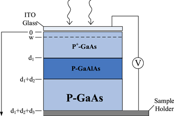
Figure 1. Schematic of surface photovoltage measurement. The light is modulated with a frequency of 120 Hz and the photovoltage is collected by the ITO glass and armor plate electrodes (d1, w, d2, d3 are the thickness values of p+-GaAs, SCR in p+-GaAs, p-GaAlAs and p-GaAs, respectively).
Download figure:
Standard image High-resolution imageThe SPV is calculated in a similar method as the photodiode open-circuit voltage [16], namely,

where r is the quality factor, kB T is the thermal energy, q is electronic charge, J0 is the dark saturation current density and Jph is the density of photogenerated current. Jph comprises a number of photogenerated current produced by the process shown by Hovel [17]. In our work, the photogennerated current density mainly comes from the three parts: the bulk of p+-GaAs, the SCR at the surface and the bulk of p-GaAs. The first part is obtained from a diffusion equation [17],

where n(x), τ, Dn, and g(x) are the concentration, lifetime, diffusion coefficient and generation rate of photogenerated minority carriers(electronics), respectively. The rate of generation can be expressed as,

where I0 is the density of photon flux, R is the value of reflectance of p+-GaAs, a1 is the absorption coefficient of GaAs, x is the distance from one point in p+-GaAs to the illuminated surface.
The boundary conditions of equation (2) in p+-GaAs bulk is in the form of

where S1 is the surface recombination velocity, S2 is the interface recombination of p+-GaAs/p-GaAlAs, and d1 is the bulk length in p+-GaAs, The diffusion current density of p+-GaAs bulk is given by

By solving equation (2), the current density of p+-GaAs bulk can be shown as,
where  LD
is the minority carriers diffusion length of p+-GaAs.
LD
is the minority carriers diffusion length of p+-GaAs.
The current density for the photogenerated carriers in the SCR,

So, the photogenerated current density provided by p+-GaAs is expressed as,

The light at short wavelength is mainly absorbed at the surface of p+-GaAs, then, only the light at longer wavelength can penetrate into the GaAlAs layer. GaAlAs can only absorb high energy photons and genenrate carriers. In our model, p+-GaAs layer is thick enough to prevent high energy from penetrating into GaAlAs layer. Here, we think GaAlAs layer can not generate carriers. And, we can obtain the incident photon flux density at the interface of p-GaAlAs/p-GaAs,

The diffusion contribution from the bulk of p-GaAs can be calculated in a similar way, the boundary conditions are given as follows,

we have the current density,

where LD ' is the diffusion length of minority carriers in p-GaAs, S3 is the interface recombination velocity of p-GaAlAs/p-GaAs, a2 is the absorption coefficient of GaAs.
Inserting J1 and J2 into equation (1), we can obtain

where J01, J02 are the dark saturation current density of p+-GaAs and p-GaAs, respectively. As J1/J01 ≪ 1 and J2/J02 ≪ 1, so

where C = rkB T/qJ01, C' = rkB T/qJ02, and VOC is the final surface photovoltage.
3. Experiment
The two Be-doped p+-GaAs/p-GaAlAs/p-GaAs samples are grown by molecular beam epitaxy (MBE). The thickness of p+-GaAs layer of sample 1 is 1.2 μm and that of sample 2 is 0.8 μm. The thickness of p-GaAs layers of two samples are 650 μm. The doping concentration of p+-GaAs is 5.22 × 1018 cm−3, while the doping concentration of p-GaAs is 5 × 1016 cm−3. If joint these two layers directly, the physical and electrical properties of GaAs may be affected due to lattice mismatch [18]. A p-GaAlAs layer whose thickness is 0.6 μm with high doping concentration of 3.44 × 1018 cm−3 and 0.63 Al mole fraction is used to match with p+-GaAs and p-GaAs layers as a buffer layer.
Prior to the SPV measured process, a wet chemical cleaning process is employed to eliminate surface contaminates of those two samples such as oxides, carbon and oil stain. Samples are firstly cleaned successively in ethanol and deionized water by ultrasonic waves for 5 min. Then, the samples are etched by a H2SO4:H2O2:H2O solution at ratios of 3:1:1 for 15 s. At last, the samples being rinsed by deionized water and dried in air are transferred to the experimental apparatus of the SPV method.
In figure 2, the light from a 75W quartz-tungsten-halogen lamp is filtered through a chopper and a grating monochromator. The light penetrates through an indium tin oxide coating deposited on glass and illuminates on the surface of the sample (figure 1). The SPV signal of the sample is detected and then amplified by the phase-locked amplifier. The light intensity is monitored by optical power meter consisting of Si photocell and picommeter and a constant photo flux can be maintained by adjusting the output current value of programmable power when wavelengths are changed from 400 to 1200 nm in the SPV spectra measurements.

Figure 2. Schematic diagram of experimental set-up of the SPV method.
Download figure:
Standard image High-resolution imageIn our experiment, we have used the front geometry to measure the SPS of the two samples, namely sample 1 and sample 2 at room temperature. In order to verify our theory model, the backside geometry is used to measure the SPS of p-GaAs.
4. Results and discussion
4.1. Comparison of the front illumination and backside illumination
The sample with backside illumination is equivalent to illuminating on a GaAs substrate surface since GaAs substrate is thick enough. Figure 3 shows the measured SPV signals of GaAs layer. The measured SPV signal depends on the equation [19]

where R' is the value of reflectance of p-GaAs surface, SV is the surface recombination velocity of p-GaAs substrate, and the other symbols of equation (14) have the same meaning as equation (13). The normalized SPV signals can be given as follows:

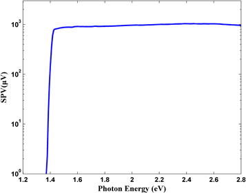
Figure 3. The experimental SPS of p-GaAs by the backside illuminating.
Download figure:
Standard image High-resolution imageThe SPVNORM of p-GaAs have been obtained by illuminating on the backside of sample 1, the experimental curve is shown in figure 3.
Then, inserting equation (14) into equation (15), we have obtained equation (16),

where K = (qJ02/rkB
T)(SV
LD
' + Dn
)/SV
LD
'2. According to equation (16), LD
' could be determined by a linear plot of  versus 1/a2.
The fitted curve was obtained by the least square method on the experimental data based on equation (16). As shown in figure 4, the value of LD ' obtained by the above method is 3.6 μm, and this method is just used to measure the minority carrier diffusion length of semiconductors which are thick enough.
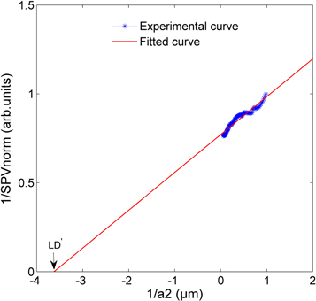
Figure 4. Curve of  (normalization) versus 1/α2 for p-GaAs substrate.
Download figure:
Standard image High-resolution imageIn our model, we would like to get the minority carrier diffusion length of semiconductor with a thinner layer in multi-layer structures. Therefore, the single layer measured method mentioned here is not suited. We have measured the SPS of the sample 1 by the front illumination.
The experimental curve of the SPS is shown in figure 5. As can be seen from the experimental curve, the photovoltage contributed by the p+-GaAs layer is smaller than the photovoltage contributed by the p-GaAs. The peak value of experimental curve appears at about 1.43 eV. The SPS curve decreases at a larger slope when the incident photon energy is larger than 1.43 eV, but when the photon energy reaches a critical value, the SPV value would keep stable at a value by increasing the photon energy, which is far smaller than the peak value. The main reason leads to the phenomenon is that the high-energy photons could be absorbed completely in the p+-GaAs layer while most low-energy photons would be absorbed by the p-GaAs owing to the thinner p+-GaAs layer.

Figure 5. The experimental SPS of p+-GaAs/p-GaAlAs/p-GaAs by the front illuminating.
Download figure:
Standard image High-resolution imageAt the same time, it is clear that the SPS of the multi-layer structure in figure 5. Has a great difference from the single-layer SPS curve in figure 4. The single-layer SPS curve is flatter and the peak value appears at the high-energy side, the photovoltage mainly originates from the diffusion of minority carrier in same semiconductor layer.
Both of the minority carrier diffusion length of the p+-GaAs layer (LD = 2.4 μm) and p-GaAs layer (LD ' = 3.7 μm) have been obtained by curve fitting according to equation (13), the other fitting parameters are listed in table 1. Compared with the LD' obtained by backside illumination, the two values are in a good agreement which proves the validity of our model and solution method.
4.2. Comparison of p+-GaAs with different thickness
To further verify our model, two samples with different thickness have been measured. The experimental curves of sample 1 and sample 2 are shown in figure 6.

Figure 6. Experimental (solid lines) and theoretical (dashed lines) SPS curves. Curves 1 and 1' represent the sample 1, curves 2 and 2' represent the sample 2.
Download figure:
Standard image High-resolution imageThe peak values of both of the experimental curves appear at about 1.43 eV. The critical value of sample 1 is about 2.1 ev while the critical value of sample 2 is about 2.3 ev. We can also consider the critical value as a photon energy threshold which p+-GaAs layer could absorb totally above it. Compared sample 1 with sample 2, the SPS of sample 1 is smaller at the low-energy side because thicker p+-GaAs layer absorbs more photons. Consequently, it is the fact that different thickness of p+-GaAs layer have different critical values, but the critical value would disappear when the thickness of the layer is enough to totally absorb the photons with the energy ranging from 1.24 to 2.8 ev, then the SPS curves would be like the curve in figure 3.
According to equation (13), we can fit the surface photovoltage spectrum curve by adopting the least-square method, where the fitting photon energy ranges from 1.24 to 2.8 ev. The fitting curves are shown in figure 6. The fitted values of material performance parameters, such as electron diffusion length LD and LD ', surface/interface recombination velocity S1, S2 and S3, the dark saturation current density J01 and J02, and the thickness of SCR at the surface w, are listed in table 1. The fitting parameters of two samples are nearly same, namely, the thickness of p+-GaAs layer has no influence on these parameters.
4.3. Analysis of some properties of the samples
The parameters calculated by curve fitting show the surface recombination velocity S1 is two orders of magnitude larger than interface recombination S2, while S3 is smaller than S1 but larger than S2. Among the three recombination velocity parameters, S1 is the largest because plenty of dangling bonds exist at the terminal surface. As the lattice constants of GaAlAs and GaAs are fitted very well, few dangling bonds and misfit dislocations generate at interface [20], a smaller interface recombination velocity S2 forms here. Zhang et al [21] has reported the back interface recombination velocity of the transmission-mode GaAs photocathodes grown by MBE, the value is 105 cm s−1. The structure of GaAs photocathodes they used is similar to our samples. The interface S3 of GaAlAs/p-GaAs is not close to S2, we think GaAs with different doping concentration may have different matching degree with GaAlAs.
Part II has presented a SCR forms at the illuminating surface inevitably in our model though a clean surface has gotten before SPV measured, the width of SCR we have obtained is listed in table 1. The width of SCR has no change when the samples with different p+-GaAs thickness at the same measured conditions. However, the effect of SCR is small when compared with the bulk diffusion. We think the width of SCR is related to surface properties, contact potential with indium-tin-oxide (ITO), it is hard to find a favorable equation to get it.
Among the parameters listed in table 1, it is very interesting to find the effect of dark saturation current density. Toušek et al has shown different semiconductors have different dark saturation current density [22]. In our experiment, the dark saturation current density of p+-GaAs is larger than the dark saturation current density of p-GaAs, we think the large ratio of dark saturation current density is the main reason that SPV at the high-energy side is far lower than SPV at the low-energy side. Figure 7. shows that increasing the ratio of J01/J02 increases the distance between the maximum and minimum of SPS. The values of J01/J02 listed in table 1 for different p+-GaAs thickness are nearly equal. Different doping concentration for the same GaAs materials may be the main reason to induce so large J01/J02.

Figure 7. Effect of different ratios of J01/J02 on the theoretical SPS calculated for the other parameters the same as curve 1 in figure 6.
Download figure:
Standard image High-resolution image
5. Conclusions
In this paper, we have investigated the SPS of p+-GaAs/p-GaAlAs/p-GaAs at room temperature. A multilayer theoretical model is established to explain the SPS of p+-GaAs/p-GaAlAs/p-GaAs. In this model, we think the photovoltage primarily originates from the minority carrier diffusion in p+-GaAs and p-GaAs. The minority carrier diffusion length in p+-GaAs and p-GaAs are obtained by fitting with the experimental SPS curves. The backside illuminating geometry was used to measure the SPV of p-GaAs and obtain the minority carrier diffusion length in p-GaAs, the single-layer GaAs experimental curve has a great difference with multi-layer experimental curves. The result shows the minority carrier diffusion length in p-GaAs measured by the front illuminating geometry as much as the backside illuminating geometry, our theoretical model is acceptable. Two samples with different p+-GaAs thickness have been measured, which show the minority carrier diffusion length and other parameters not influenced by the thickness. Analysis of the dark saturation current density shows that it has a great influence on SPS curves of multi-layer structures.
Acknowledgments
This work is supported by the National Natural Science Foundation of China (Grant No. 61605180), Shandong Provincial Natural Science Foundation (Grant No. ZR2019MF010) and Science and Technology Program for Higher Education of Shandong Province (Grant No. J18KA320).