
Abstract
The energy bands, density of states, charge density, Mulliken population, equation of state and elastic properties of α-CdP2 have been studied. Exchange correlation functional PBEsol is utilized in this study. The optimized equilibrium lattice parameters of the conventional cell have been obtained. The present investigation indicates the existence of an indirect band gap of 1.76 eV in α-CdP2 crystal. Elastic calculations show the mechanical stability of the alpha phase of CdP2 crystal. This work provides an analysis of directional Young's modulus and linear compressibility for α-CdP2. The study of the elastic anisotropy parameters shows that the alpha phase has a definite elastic anisotropy. The calculated Debye temperature of α-CdP2 is 288.1 K.
Export citation and abstract BibTeX RIS

Original content from this work may be used under the terms of the Creative Commons Attribution 4.0 licence. Any further distribution of this work must maintain attribution to the author(s) and the title of the work, journal citation and DOI.
1. Introduction
Cadmium diphosphide (II-V2 group semiconducting compound) is reported to be a good feasible material for device application in the field of optoelectronics [1–3] and thermal sensors [4]. The optical properties of CdP2 enable it to be used in the fabrication of solar cells [5]. CdP2 is also useful as a dopant compound for the fabrication of nGaAs/InP PIN photodetector arrays by the metal-organic chemical vapor deposition technique [6]. CdP2 exists in two different crystalline phases, namely alpha and beta [7]. The alpha phase of CdP2 is an orthorhombic structure at room temperature [7]. The α-CdP2 crystal structure has a space group Pna21 with four formula units in the conventional unit cell [8]. A pronounced structural character in the alpha phase of CdP2 is a helical ![${}_{\infty }{}^{1}[{P}^{-}]$](https://content.cld.iop.org/journals/2053-1591/7/9/095901/revision3/mrxabb0adieqn1.gif) -chain coordinated to cadmium ions [7]. The peculiarity of the α-CdP2 structure is chains of P atoms existing parallel to each other in the
c
direction in the crystal [9]. DFT calculation showed the piezoelectricity in the alpha phase of CdP2 [10–12]. This piezoelectric characteristic opens the doors for the future possibility of using α-CdP2 in designing piezoelectric devices such as piezoelectric sensors, transducers, etc. The piezoelectric effect is closely related to basic mathematical formulations based on elastic stiffness constants and dielectric susceptibility. Our elastic characterization and interpretation may get considerable practical utility in the field of piezoelectric device technology for future research. The experimental and theoretical investigations of tetragonal β-CdP2 have been carried out by several researchers [13–16]. To the best of our knowledge, thorough experimental and theoretical investigations of the alpha phase of CdP2 have not yet been reported. The first principle method within density functional theory has been applied to explore the structural properties, energy bands, density of states, charge density, Mulliken population [17] and elastic properties of α-CdP2. Our present ab initio study is able to explore the unrevealed properties of α-CdP2. Our attempt to fill the existing research gap in the study of the alpha phase of CdP2 crystal is likely to be advantageous for researchers to carry out further investigations for application in optoelectronics and piezoelectric device technologies. The article thereon is organized as follows: In section 2, computational techniques are described. This is followed by results and discussion in section 3. Finally, we discuss conclusions in section 4.
-chain coordinated to cadmium ions [7]. The peculiarity of the α-CdP2 structure is chains of P atoms existing parallel to each other in the
c
direction in the crystal [9]. DFT calculation showed the piezoelectricity in the alpha phase of CdP2 [10–12]. This piezoelectric characteristic opens the doors for the future possibility of using α-CdP2 in designing piezoelectric devices such as piezoelectric sensors, transducers, etc. The piezoelectric effect is closely related to basic mathematical formulations based on elastic stiffness constants and dielectric susceptibility. Our elastic characterization and interpretation may get considerable practical utility in the field of piezoelectric device technology for future research. The experimental and theoretical investigations of tetragonal β-CdP2 have been carried out by several researchers [13–16]. To the best of our knowledge, thorough experimental and theoretical investigations of the alpha phase of CdP2 have not yet been reported. The first principle method within density functional theory has been applied to explore the structural properties, energy bands, density of states, charge density, Mulliken population [17] and elastic properties of α-CdP2. Our present ab initio study is able to explore the unrevealed properties of α-CdP2. Our attempt to fill the existing research gap in the study of the alpha phase of CdP2 crystal is likely to be advantageous for researchers to carry out further investigations for application in optoelectronics and piezoelectric device technologies. The article thereon is organized as follows: In section 2, computational techniques are described. This is followed by results and discussion in section 3. Finally, we discuss conclusions in section 4.
2. Computational details
In this study, all the calculations are performed with CRYSTAL Program [18, 19] which is an ab initio quantum mechanical program. CRYSTAL Program (periodic ab initio HF and DFT code) uses a localized Gaussian type basis set to form the sets of Bloch functions. In this computational work, the DFT exchange-correlation functional GGA (Generalized Gradient Approximation) is implemented. The study of geometrical optimization, EOS (equation of state), bands, DOS (density of states), Mulliken population and elastic constants is carried out with PBEsol [20] method. The basis sets (for Cd and P atoms) have been employed from CRYSTAL-basis set library of Torino group [18, 19]. We use the basis set of 36 orbitals for Cd atom [21] and the basis set of 18 orbitals for P atom [22]. The calculations are performed using an 8 × 8 × 8 Monkhorst-Pack k-point mesh [23] that corresponds to 125 k-points in the irreducible Brillouin zone (IBZ). The SCF convergence threshold on the total energy is set to 10–10 Hartree. The BROYDEN parameter [18, 19, 24, 25] is employed to achieve the rapid convergence of the self-consistent iterations. The Fock/Kohn–Sham matrix mixing factor (FMIXING) [18, 19] of 40% has become useful for the calculations of geometry optimization. The optimized structure is utilized to determine bulk modulus and its first pressure derivative by deploying the EOS within ±8% variation of the volume of optimized geometry. Furthermore, electronic and elastic properties [26, 27] are investigated at the equilibrium volume. The magnitude of the strain step for elastic calculations is 0.01. The unit cell is drawn using DLV software [28]. We use a web-oriented tool CRYSPLOT [29] for charge density and energy band structures.
3. Results and discussion
3.1. Structural details
The structure of α-CdP2 comes under the orthorhombic space group Pna21 with approximate values of lattice parameters a = 9.90 Å, b = 5.408 Å and c = 5.171 Å [8]. Its unit cell consists of four Cd and eight P atoms [8]. Using the available geometry of α-CdP2 [8], we have obtained the optimized lattice parameters and fractional coordinates of the atoms for the unit cell of α-CdP2 as shown in the tables 1 and 2. The deviations in the calculated lattice parameters (a, b and c) from the experimental values [8] are within 1.6% and deviation in conventional cell volume is 2.43%. From table 1, it is obvious that our calculation of cell volume of ≈283.57 Å3 is in accordance with other DFT work [15] with a small deviation of 0.86%. Thus, our computed results are in good agreement with the other reported results in tables 1 and 2. The unit cell of α-CdP2 with optimized lattice parameters is shown in figure 1. There exist deformed tetrahedral bonds [8] as depicted in figure 1. Each cadmium atom is bonded to its four nearest phosphorus atoms. It is also evident from figure 1 that each P atom is bonded to two nearest Cd atoms and two nearest P atoms. Table 5 shows that atom P5 (nonequivalent atom P-I) has the first four nearest neighbors P10, P9, Cd3 and Cd1 atoms. Atom P9 (nonequivalent atom P-II) has the first four nearest neighbors P6, P5, Cd1 and Cd2 atoms.
Table 1. The lattice parameters (a, b and c in Å) and volume V (Å3) of the conventional cell of α-CdP2.
| Scheme | a | b | c | V | |
|---|---|---|---|---|---|
| Present work | PBEsol | 10.0051 | 5.4924 | 5.1603 | 283.5689 |
| Exp. a | 9.90 | 5.408 | 5.171 | 276.85 | |
| Other work b | 286.0 |
Table 2. The fractional coordinates of the nonequivalent atoms in the unit cell of α-CdP2.
| Atom | Fractional coordinates | ||||||||
|---|---|---|---|---|---|---|---|---|---|
| Present work (PBEsol scheme) | Exp. a | Other work b | |||||||
| X/a | Y/b | Z/c | X/a | Y/b | Z/c | X/a | Y/b | Z/c | |
| Cd | 0.1502 | 0.1050 | 0.2621 | 0.1529 | 0.1016 | 0.2606 | 0.1529 | 0.1011 | 0.2606 |
| P (I) | 0.1222 | 0.4441 | –0.3924 | 0.1186 | 0.4458 | 0.5850 | 0.1185 | 0.4442 | 0.5957 |
| P (II) | –0.0091 | 0.2722 | –0.0916 | –0.0074 | 0.2697 | –0.0676 | –0.0064 | 0.2693 | –0.1036 |

Figure 1. Schematic representation of the crystal structure of α-CdP2. The lengths a, b and c are lattice parameters. (a) Schematic 3D view of the conventional cell of α-CdP2. (b) Side view (ab plane) of α-CdP2 crystal structure. (c) Side view (ac plane) of α-CdP2 crystal structure. (d) Side view (bc plane) of α-CdP2 crystal structure.
Download figure:
Standard image High-resolution image3.2. Equation of state
In this study, the EOS computations for the alpha phase are performed using its computed optimized lattice parameters and fractional coordinates of atoms. The isothermal bulk modulus  and its first pressure derivative
  are computed using Vinet [30], Poirier-Tarantola [31] and Birch-Murnaghan [32] EOSs. These estimated values of
  and
and  are shown in table 3. In this present work, it is evident from table 3 that our computed values of
  and
and  of α-CdP2 at zero pressure with Vinet, Poirier-Tarantola and Birch-Murnaghan EOSs are ≈57.88 GPa and ≈3.94, respectively. Almost the same findings each for
 and V0 (equilibrium cell volume) are obtained using these three EOS schemes. For the unit cell of the alpha CdP2, with respect to minimum energy, the curve of relative energy E (per unit cell) against its cell volume is plotted by means of Vinet EOS as shown in figure 2. The quantities
  and
and  are not mere coefficients in the equation of states, furthermore, they are physical characteristics of the materials which depend on the structural composition of the materials [33]. The most common typical range of
  for solid materials is from 2 to 6 [33], so obtained value 3.94 of
  for α-CdP2 is quite physically reasonable in this study.
Table 3. Bulk moduli ( ), their first pressure derivatives (
 ) and equilibrium cell volumes (V0) of α-CdP2 at zero pressure using PBEsol scheme.
| EOS method |
 (GPa) (GPa) |

| V0 (Å3) | |
|---|---|---|---|---|
| Present work | Vinet | 57.88 | 3.94 | 283.5264 |
| Present work | Poirier-Tarantola | 57.92 | 3.94 | 283.5254 |
| Present work | Birch-Murnaghan | 57.83 | 3.93 | 283.5277 |

Figure 2. The variation of relative energy E (per unit cell) of α-CdP2 with its cell volume taking the minimal value in the set of calculations as zero. The curve shows the Vinet EOS fits the computed data points ( ) in the approximate range of 261 Å3 to 305 Å3.
Download figure:
Standard image High-resolution image3.3. Band structure and DOS
A study of electronic structure and density of states is useful in the determination of the semiconducting properties of a material. In figure 3, the electronic band structure is plotted along suitable paths connecting eight special points of high symmetry [23, 34] in the reciprocal space. The highest point of the valance band lies on a path  and the lowest point of conduction band lies close to X point in the reciprocal space. Figure 3 indicates the existence of an indirect band gap, Eg of 1.76 eV in the orthorhombic phase of CdP2. The value 1.76 eV falls within the typical range of energy band gap of semiconductor substances. A band gap of 1.439 eV was reported in other computational work [10, 11].
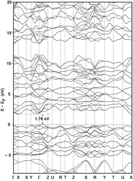
Figure 3. Under PBEsol scheme, the energy band structure of α-CdP2 (in the range of –8 to 20 eV relative to Fermi energy level EF).
Download figure:
Standard image High-resolution imageTo reveal the distribution of electronic states, the computed total DOS along with the partial density of states (PDOS) of Cd and P atoms are depicted in figure 4. In the immediate vicinity of the top of the valence band region and the bottom of the conduction band region, p orbitals of phosphorus atoms predominantly contribute to DOS. With regard to DOS, the contribution of P(II) atom, in general, is larger than that of P(I) atom, but overall PDOS patterns due to the individual nonequivalent P atoms are broadly similar. We pay particular attention to DOS lying near the Fermi level, as these DOS are important with reference to the electronic properties of solids. In our investigation, we also observed about PDOS that chiefly p orbitals of the second and third sp shells (shown in table 4) of phosphorus atoms contribute to DOS lying near the Fermi level in the valence region and furthermore, the contribution of the third sp shell (having more diffused orbitals) is larger than that of the corresponding second sp shell of that P atom. Besides, contribution to DOS from Cd atoms is relatively low at the top of the valence band as well as at the bottom of the conduction band. Hence, the top of the valence band and the bottom of the conduction band are mostly of P-p characters.

Figure 4. The plot of total DOS along with contributions from s, p and d orbitals of the nonequivalent atoms of α-CdP2 (in the range of –5 to 7.5 eV relative to Fermi energy level EF). On the y-axis all arb. units are identical. Fermi level is shown by vertical dashed lines at 0 eV.
Download figure:
Standard image High-resolution imageTable 4. Mulliken population analysis for α-CdP2 using PBEsol method. Charges are indicated in the unit of elementary charge e.
| Cd | P(I) | P(II) | ||||||
|---|---|---|---|---|---|---|---|---|
| Total charge (N. electrons) = 46.977 | Total charge (N. electrons) = 15.522 | Total charge (N. electrons) = 15.502 | ||||||
| Orbital No. | Shell | Shell charge | Orbital No. | Shell | Shell charge | Orbital No. | Shell | Shell charge |
| 1 | s | 2.000 | 145 | s | 2.000 | 217 | s | 2.000 |
| 2–5 | First sp | 7.998 | 146–149 | First sp | 7.824 | 218–221 | First sp | 7.824 |
| 6–9 | Second sp | 7.983 | 150–153 | Second sp | 2.000 | 222–225 | Second sp | 2.001 |
| 10–14 | d | 9.994 | 154–157 | Third sp | 3.657 | 226–229 | Third sp | 3.637 |
| 15–18 | Third sp | 6.539 | 158–162 | d | 0.042 | 230–234 | d | 0.041 |
| 19–22 | Fourth sp | 1.426 | ||||||
| 23–26 | Fifth sp | 1.077 | ||||||
| 27–31 | d | 8.767 | ||||||
| 32–36 | d | 1.193 | ||||||
3.4. Charge density and Mulliken population analysis
The computed total electron density map for (010) plane is shown in figure 5. The isodensity contour lines for the total electron density map are sketched at intervals of 0.02 e/Bohr3. Furthermore, the total distribution of electronic charge density is predicted through the Mulliken population analysis. There exist two crystallographically nonequivalent distinct sites of P atom, therefore the charge distribution is accordingly influenced by the orientation of the respective atom in the unit cell, as evident from table 4. In the present investigation, CRYSTAL Code shows 288 orbitals for the unit cell. In table 4, orbitals and shells along with corresponding charges are shown and it is obvious that there is also a small charge transfer of about 0.041e to d shell of the associated basis set of each P atom in the α-CdP2 crystal.

Figure 5. Computed total electron density map of α-CdP2 for (010) plane using PBEsol method. Lattice parameters a = 10.0051 Å and c = 5.1603 Å.
Download figure:
Standard image High-resolution imageMany physical properties of a material are correlated to its constituent chemical bonds. Mulliken population analysis plays an important role to predict the characteristics of the chemical bonding in the materials. Mulliken overlap populations for α-CdP2 are illustrated in table 5. The positive value of the total overlap population corresponds to bonding, whereas the negative value of the total overlap population corresponds to antibonding [17]. Mulliken population analysis is an important tool for the estimation of the distribution of charges in the atomic orbitals. In our study, for the one formula unit of α-CdP2, there is total charge transfer of about 1.02 electrons from one Cd atom to two P atoms as evident from table 4. On the basis of the result of charge transfer, an approximated effective valence state of α-CdP2 may be represented as  Thus, it indicates the reasonable presence of ionic character in the Cd-P bonding. The Mulliken overlap population also provides a good estimation of the covalent bonding [17]. A high level of overlap population reflects the high level of covalent character of a chemical bond [35]. In the present study, the overlap population between Cd atom and immediate neighboring P atom is about 0.14 as shown in table 5. This value 0.14 is reasonably small compared to 1 and it can be inferred that the Cd-P bonds are also partially covalent in nature. The present study suggests the existence of mixed ionic-covalent character of bonds (Cd-P) in the alpha phase of CdP2. Furthermore, the Mulliken overlap population is useful to reflect its correlation with the strength of the bond. A comparison of hardness
  of the bonds (between Cd atom and its immediate neighboring P atoms) is carried out using the expression
  [36] where,
  and
and  denote, respectively, the volume and Mulliken overlap population of the μ type bond and A is the proportional coefficient. In the present study, results show that the computed hardness of bonds Cd1-P7, Cd1-P9, Cd1-P5 and Cd1-P10 are in the ratio 1.254 : 1.082 : 1.094 : 1.000. The higher level of hardness of the bond Cd1-P7 among these mentioned Cd-P bonds may be attributed to its relatively high Mulliken overlap population and short bond length.
Table 5. Mulliken overlap populations for α-CdP2 using PBEsol scheme.
| Atomic pair AB | Distance AB (Å) | Overlap population AB |
|---|---|---|
| Cd1-P7 | 2.569 | 0.154 |
| Cd1-P9 | 2.592 | 0.139 |
| Cd1-P5 | 2.594 | 0.141 |
| Cd1-P10 | 2.618 | 0.135 |
| Cd1-P6 | 3.768 | – 0.009 |
| P5-P10 | 2.183 | 0.068 |
| P5-P9 | 2.242 | 0.021 |
| P5-Cd3 | 2.569 | 0.154 |
| P5-P6 | 3.608 | – 0.066 |
| P5-Cd2 | 3.768 | – 0.009 |
| P9-P6 | 2.183 | 0.068 |
| P9-Cd2 | 2.618 | 0.135 |
| P9-P10 | 3.599 | – 0.069 |
As reported by Olofsson and Gullman [9], the bond distance (Cd-P) between close neighbor cadmium and phosphorus atoms ranges from 2.562 Å to 2.619 Å and the bond distance (P-P) between close neighbor phosphorus atoms ranges from 2.167 Å to 2.20 Å. It is evident from table 5 that our calculated values of bond distances are in fair agreement with the mentioned ranges [9].
3.5. Elastic properties
3.5.1. Elastic constants and mechanical stability
The study of elastic properties is extremely useful for understanding the ability of the material to resist the deformation. The direction-dependent elastic stretchability of crystals under different tensile strains can shed light on its advantages for engineering applications. A high value of the ratio of bulk modulus to shear modulus enables the crystal to meet various requirements of curvilinear shape for practical applications. Also, piezoelectricity is dependent on the intermingling of elastic and electric phenomena. In view of the device application of α-CdP2 crystal, it is necessary to estimate its elastic constants so that its mechanical stability and elastic properties may be examined. The orthorhombic crystal system has nine independent elastic stiffness coefficients due to its orthorhombic symmetry [37]. These computed elastic stiffness coefficients Cij of α-CdP2 are reported in table 6. According to Mouhat et al [38], necessary and sufficient elastic stability conditions for an orthorhombic system are given by the following expressions [from (1) to (3)]:


The computed elastic stiffness constants (given in table 6) satisfy these necessary and sufficient elastic stability conditions for the orthorhombic system. It shows the mechanical stability of the alpha phase of CdP2 crystal.
Table 6. Elastic stiffness constants (in GPa) of α-CdP2 at zero pressure.
| Scheme | C11 | C12 | C13 | C22 | C23 | C33 | C44 | C55 | C66 | |
|---|---|---|---|---|---|---|---|---|---|---|
| Present Work | PBEsol | 105.163 | 50.352 | 43.412 | 86.520 | 41.857 | 74.230 | 33.418 | 24.329 | 27.482 |
| Other Work a | PBE | 101.3 | 31.1 | 37.7 | 91.4 | 32.5 | 87.3 | 37.4 | 28.2 | 19.0 |
a Reference [15].
In terms of elastic stiffness constants Cij and elastic compliance constants Sij , more quantities such as bulk modulus, shear modulus and Poisson's ratio may be represented. Voigt bulk modulus BV and Reuss bulk modulus BR can be expressed as [39, 40]


Similarly, Voigt shear modulus GV and Reuss shear modulus GR are given by [39, 40]


According to the Voigt-Reuss-Hill approximation, polycrystalline bulk and shear moduli can be estimated as [39–41]


Macroscopic polycrystalline Young's modulus EH and Poisson's ratio  can be expressed as [39–41]


To investigate the mechanical properties of α-CdP2, various elastic moduli are determined from elastic constants and are summarized in table 7. The value of bulk modulus is 58.745 GPa which indicates that the material has sufficient mechanical strength to resist structural deformation. The Cd crystal has bulk modulus of ≈46.7 GPa [42] and Young's modulus of ≈62.3 GPa [42]. The values of bulk modulus and Young's modulus for orthorhombic P crystal are ≈36 GPa [43] and ≈30.4 GPa [42] respectively. It can be seen in table 7 that the calculated values of Young's modulus and bulk modulus of α-CdP2 are greater than the respective values of Young's moduli and bulk moduli of constituent elements (Cd and P crystals). But, in comparison to the typical values of bulk modulus ≈97.8 GPa [44] and Young's modulus ≈163 GPa [45] of the semiconductor Si, it is obvious that our calculated respective values of bulk modulus 58.745 GPa and Young's modulus 66.219 GPa of α-CdP2 are considerably smaller. Since Young's modulus reflects the stiffness of the material, so α-CdP2 crystal has less stiffness than Si crystal.
Table 7. Using PBEsol method, computed values of bulk modulus B (in GPa), shear modulus G (in GPa), Young's modulus E (in GPa), Poisson's ratio  (unitless) of α-CdP2 according to Voigt-Reuss-Hill notations
a
.
(unitless) of α-CdP2 according to Voigt-Reuss-Hill notations
a
.

|

|

|

|

|

|

|

|

|

|

|

| |
|---|---|---|---|---|---|---|---|---|---|---|---|---|
| Present work | 59.684 | 57.807 | 58.745 | 25.732 | 24.735 | 25.233 | 67.496 | 64.942 | 66.219 | 0.3115 | 0.3128 | 0.3121 |
a
Values of B, G, E and  have been obtained using ELATE software [46, 47].
It is also obvious from table 7 that the values of computed Poisson's ratios are about 0.31. Therefore these calculated values of Poisson's ratios are within the theoretically essential limits [48] for materials. In general, the ratio of bulk modulus B to shear modulus G may be used to make predictions about the nature of polycrystalline material in terms of brittleness and malleability [49]. A high value of B/G indicates the malleable nature of the polycrystalline materials [49]. For a value of B/G greater than about 1.75, malleable characteristics of a polycrystalline material is expected [49]. In the present study, the value of BH/GH is 2.328 which is greater than 1.75, therefore it indicates the malleable nature of α-CdP2. Thus the value 2.328 of B/G for the alpha phase of CdP2 crystal indicates that the crystal has reasonable malleability and this favorable property opens the possibility to allow the curved shape of α-CdP2 crystal in the semiconductor devices.
3.5.2. Elastic anisotropy
Most of the materials show elastic anisotropic behavior. Atomic bonding arrangement in different crystalline planes is an important factor for the determination of the elastic anisotropy. Elastic anisotropy plays a key role in various directional dependent mechanical-physical phenomena. Elastic constants such as Young's modulus, shear modulus and Poisson's ratio may have directional dependent variations, hence they have an influence on the mechanical characteristics of the crystalline materials. With the help of the theory of micro-cracks analysis from the elastic anisotropy, the enhancement in the mechanical durability of the crystals for device application may be understood [50]. A comprehensive understanding of the elastic anisotropy of the materials is of great significance because it has an important outlook for device designing. The preferred orientation of the crystals is a vital aspect for optimum technological usage of the materials in microelectromechanical systems, hence the knowledge of the elastic anisotropy is essential for imparting the desired physical and electrical properties to devices. For an orthorhombic crystal system, the directional Young's modulus E in the direction of the unit vector li is given by the expression [37]

where l1, l2 and l3 are direction cosines and quantity Sij are known as elastic compliance constants.
For an orthorhombic crystal system, the directional linear compressibility β in the direction of the unit vector li is given by the expression [37]

Table 8 shows the computed Young's Modulus and linear compressibility of α-CdP2 along [100], [010] and [001] crystallographic directions. Figure 6 shows the variations of Young's modulus with direction. Figures 6(a) and 7(a) are plotted using ELATE software. It is evident from the figures 6(a) and 7(a) that schematic plots of directional Young's modulus and linear compressibility are not spherical in shape; therefore, they reflect the finite elastic anisotropy for the alpha phase of CdP2. The elastic anisotropy of a crystal may be characterized by different approaches. For instance, to compute the elastic anisotropy, the degree of elastic anisotropy may be defined by expressions [51, 52]


For elastic isotropic materials, both AB and AG are zero. Our calculated values of AB and AG for the degree of elastic anisotropy are shown in table 8. It is evident from table 8 that values of AB and AG are nonzero, therefore, α-CdP2 crystal has finite bulk anisotropy as well as shear anisotropy. In different way, Ranganathan et al [53] defined the universal elastic anisotropy index as

The index AU is applicable to all crystalline symmetry and its minimum value is zero for elastic isotropic materials [53]. Table 8 shows the calculated value of 0.234 of AU for the alpha phase of CdP2. Both tables 8 and 9 illustrate the presence of finite elastic anisotropy characteristics in α-CdP2.
Table 8. The computed values of directional Young's modulus, linear compressibility and elastic anisotropy parameters for α-CdP2 under PBEsol scheme.

|

|

|

|

|

|

|

|

| |
|---|---|---|---|---|---|---|---|---|---|
| Present work | 69.135 | 54.526 | 49.195 | 3.411 | 5.529 | 8.359 | 1.60 | 1.98 | 0.234 |
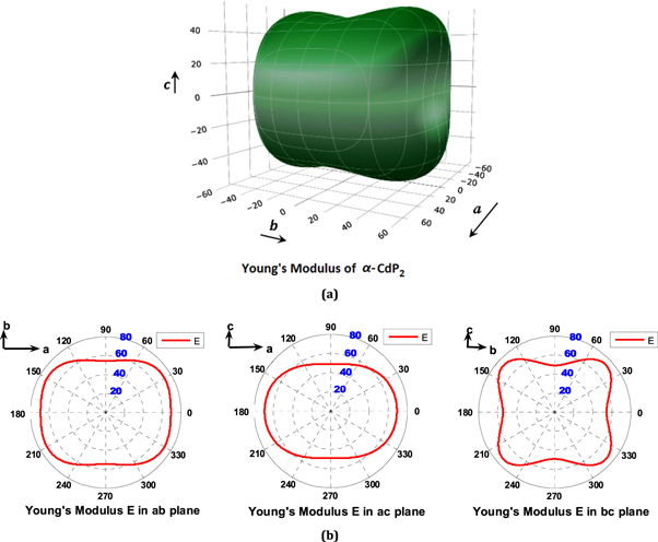
Figure 6. Directional dependence (polar graph) of the computed Young's modulus E (in GPa) of α-CdP2. (a) 3D View representation of directional Young's modulus (b) Projections of directional Young's modulus on ab, ac and bc planes.
Download figure:
Standard image High-resolution image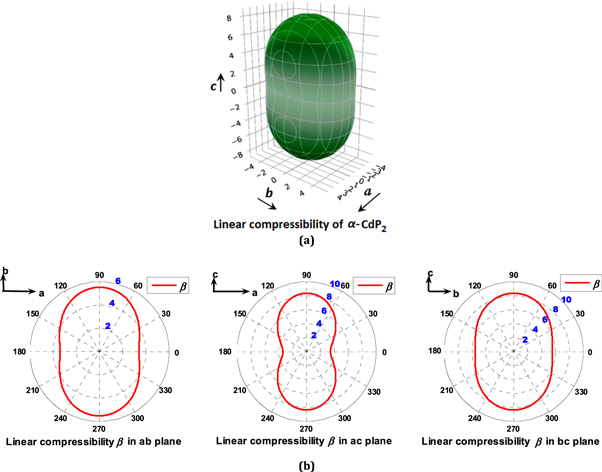
Figure 7. Directional dependence (polar graph) of the computed linear compressibility β [in (TPa)−1] of α-CdP2. (a) 3D View representation of directional linear compressibility (b) Projections of directional linear compressibility on ab, ac and bc planes.
Download figure:
Standard image High-resolution image
Table 9. Variations of the shear modulus G (in GPa), Young's modulus E (in GPa), linear compressibility β [in  ] and Poisson's ratio
  (unitless) of α-CdP2 using PBEsol method
a
.
(unitless) of α-CdP2 using PBEsol method
a
.

|

|

|

|

|

|

|

| |
|---|---|---|---|---|---|---|---|---|
| Present work | 19.087 | 33.418 | 49.195 | 73.140 | 3.411 | 8.359 | 0.0908 | 0.4179 |
a
Minimum and maximum values of G, E, β and  have been obtained using ELATE software.
Significant differences are found among the computed values of E100, E010 and E001 as shown in table 8. From figures 6 and 7 as well as from table 8, the following conclusions about directional Young's modulus and linear compressibility of α-CdP2 crystal are drawn:


Hence, crystal has more hardness (less compressible) along a axis than along b and c axes. It is evident from table 9 that there is a substantial difference between the minimum and maximum values of the directional shear modulus G. This is also the case for Young's modulus E and linear compressibility β. For G, E and β, respective maximum variations are 75.08%, 48.67% and 145.06% relative to their minimum values. These variations themselves reveal the presence of considerable elastic anisotropy in the alpha phase of CdP2.
For Young's modulus E, it is readily apparent from the figure 6(b) that anisotropy is greater in bc plane than in ab and ac planes, since the angular variation of E in bc plane is more pronounced among ab, bc and ac planes. In ab plane, E increases from 69.135 GPa to ≈72 GPa (maximum value in ab plane) as the angle (with a axis) increases from 0° to ≈31°, then E decreases from ≈72 GPa to 54.526 GPa as the angle varies from ≈31° to 90°. The maximum value ≈72 GPa of E is again observed at an angle (with a axis) of ≈149° in the ab plane. It is observed in the ac plane that E decreases continuously from 69.135 GPa to 49.195 GPa (Emin in table 9) as the angle (with a axis) increases from 0° to 90°. In the bc plane, E increases from 54.526 GPa to 73.140 GPa as the angle (with b axis) increases from 0° to ≈47°. Furthermore, as the angle increases from ≈47° to 90° in the bc plane, the value of E decreases from 73.140 GPa to 49.195 GPa (Emin in table 9). The maximum value 73.140 GPa (Emax in table 9) of E is observed at the angles (with b axis) of ≈47° and ≈133° in bc plane.
In the case of linear compressibility β, it emerges clearly from figure 7(b) that the ac plane has greater anisotropy than ab and bc planes. For the ab plane, β increases continuously from 3.411 (TPa)−1 (βmin in table 9) to 5.529 (TPa)−1 as the angle (with a axis) increases from 0° to 90°. In ac plane, an increase of the angle (with a axis) from 0° to 90° results in a continuous increase of linear compressibility β from 3.411 (TPa)−1 to 8.359 (TPa)−1 (βmax in table 9). In the case of bc plane, as the angle (with b axis) varies from 0° to 90°, β increases continuously from 5.529 (TPa)−1 to 8.359 (TPa)−1. The different types of physical quantities may have different levels of anisotropy corresponding to a given plane of the same material. The present investigation shows that among ab, ac and bc planes, the anisotropy is high in ac plane for linear compressibility, whereas the anisotropy is high in bc plane for Young's modulus.
3.5.3. Debye temperature
Debye temperature, which is a useful variable, correlates the thermodynamic properties with elastic properties of the crystal [54]. The Debye temperature of the material is related to its thermal conductivity [55]. Thermal conductivity is an important parameter for heat transfer phenomena. Hence, concerning the dissipation of heat, the thermal conductivity is a significant factor for determining the speed and efficiency of the electronic devices. The Debye temperature is a function of the aggregate elastic properties (polycrystalline bulk modulus BH and shear modulus GH) [54]. The Debye temperature  is related to average sound velocity
  in a crystal by the expression [54]

where h is Planck's constant, NA is Avogadro's constant,  is the density, k is Boltzmann's constant, M is the molecular mass, n is the number of atoms in the molecule. Average sound velocity
  in a polycrystalline substance may be expressed as [54]

where  and
and  represent the average shear and longitudinal sound velocities, respectively. These velocities may be expressed in terms of density ρ, polycrystalline bulk modulus BH and shear modulus GH [54]:


For the alpha phase of CdP2, the calculated values of mean sound velocity and Debye temperature are 2769 m s–1 and 288.1 K respectively. The calculated values of shear sound velocity and longitudinal sound velocity are given in table 10.
Table 10. The computed values of density, Debye temperature, shear sound velocity, longitudinal sound velocity and average sound velocity of α-CdP2 under PBEsol method.
| ρ(kg m−3) | νs (m s−1) | νl (m s−1) | νm (m s−1) | θD (K) | |
|---|---|---|---|---|---|
| Present work | 4119 | 2475 | 4736 | 2769 | 288.1 |
4. Conclusions
The present study presents the first principle investigation of electronic and elastic properties of α-CdP2 by employing GGA-PBEsol functional in the CRYSTAL code. The obtained equilibrium volume of the unit cell is in quite agreement with experimental data. Our work predicts the existence of the indirect band gap of 1.76 eV in α-CdP2 crystal. The p orbitals of phosphorus atoms make the major contribution to DOS lying at the top of the valence band and the bottom of the conduction band. Broadly speaking, P(II) atom contributes more to DOS in comparison to P(I) atom. Mulliken population analysis shows that the total charge transfer of nearly 1.02 electrons takes place from one Cd atom to two P atoms in each formula unit of α-CdP2. Mulliken population analysis also indicates that Cd-P bonds have mixed ionic-covalent characters. Our investigation reveals that the Cd1-P7 bond has a higher level of hardness among Cd1-P7, Cd1-P9, Cd1-P5 and Cd1-P10 bonds.
Our present findings of anisotropic properties may contribute to better predictions for the preferred orientation of crystals for designing optoelectronic devices. In this investigation, the computed value of Ranganathan's universal elastic anisotropy index AU is 0.234. The considerable variation is observed among the computed values of directional Young's moduli E100, E010 and E001. It can be inferred from the present investigation that the alpha phase of CdP2 has definite elastic anisotropy and crystal is more hard (less compressible) along a axis than along b and c axes. Among ab, ac and bc planes, the anisotropy is high in bc plane for Young's modulus, whereas the anisotropy is high in ac plane for linear compressibility. The present study indicates the malleable nature of the alpha phase of CdP2. The computed value of Debye temperature of α-CdP2 is 288.1 K. The Quite adequacy of the values of Debye temperature and elastic moduli is in favor of α-CdP2 to become a promising material for device application in optoelectronics. Hence, these findings provide an outlook for experimental implications.
Acknowledgments
The author (K Kabra) is thankful to the Department of Science and Technology (DST), New Delhi, India for financial support under the WOS-A scheme via project no. SR/WOS-A/PM-032/2017, dated 04-01-2018.