
Abstract
Pulsar navigation, to meet the physical needs of detecting pulsed x-ray contour, requires a large-area and high-energy resolution silicon drift detector (SDD). Until recently when we designed and fabricated a 314 mm2 double-sided spiral SDD, SDDs developed worldwide have been relatively small in size with a typical diameter less than 10 mm. The details of the design of our 314 mm2 double-sided spiral SDD had been reported in the literature (Li (2013) Nuclear Instruments and Methods in Physics Research A 730 73–78). Present work involves the analysis of electrical characteristics simulations of a 314 mm2 double-sided spiral SDD. It is essential to study the carriers drift behavior of a 314 mm2 double-sided spiral SDD for the structural design optimization of the detector. Therefore, this paper analyzes the relevant electrical characteristics that can characterize the carriers drift behavior. Firstly, this paper illustrates the electric potential, electric field, and electron concentration of the detector. Then, it also provides an analysis of the transient current by simulated the single event transient (SET) effect. The SILVACO TCAD simulator was used to simulate these electrical characteristics. Based on TCAD simulation, the best drift electric field and optimal electron drift channel in a 314 mm2 double-sided spiral SDD are demonstrated. Moreover, the transient current and charge collection mechanism of the detector is also analyzed. Finally, we also tested the leakage current and capacitance of the detector at room temperature.
Export citation and abstract BibTeX RIS

Original content from this work may be used under the terms of the Creative Commons Attribution 4.0 licence. Any further distribution of this work must maintain attribution to the author(s) and the title of the work, journal citation and DOI.
1. Introduction
The silicon drift detector (SDD), based on the sideward depletion principle, was proposed by Gatti and Rehak in 1983 [1]. SDDs are widely used in high energy physics, aerospace, pulsar navigation, and other fields [2] because of their advantages of fast response time, high sensitivity, and energy resolution. Moreover, SDDs do not need liquid nitrogen refrigeration. They can work normally when cooled to −10 to −35 °C by simple semiconductor temperature difference refrigeration. The traditional SDD structure, built on an N-type lightly doped substrate, has a central collecting anode and circular (quad or hexagonal) P-type heavily doped concentric rings on the front side, a P-type heavily doped surface on the backside. The normal operation of the traditional SDD requires an external voltage divider to form a lateral drift electric field, which causes the electrons generated by an incident particle to drift laterally to the collecting anode. The most significant advantage of this carrier transit method is that the anode capacitance of the detector is minimal, usually around 100 fF, and independent of the size of the detector. Because it is not easy to make a suitable voltage divider, the concept of a spiral biasing adapter was proposed by Brookhaven National Laboratory [3]: one with spiral SDD cathode rings and one with SDD concentric cathode rings combining spiral biasing adapter (SBA-SDD system) [4]. Besides, our team is also trying to do a voltage divider with an implanted resistor in the concentric SDD. This method uses atomic deposition to implant resistors in the concentric SDD to form a suitable potential gradient. Still, it is not mature due to the difficulty in the design and fabrication technologies.
The rectifying junction and voltage divider of the SBA-SDD system are separated. The SBA was designed as a double-side spiral structure. In order to create a potential gradient for carriers, the ring pitch and width of the SBA and SDD must be considered comprehensively in the design of the system. An SBA can be applied to a single concentric SDD or a concentric SDD array. Usually, SBA and SDD are made on the same silicon substrate, and SBA and SDD are connected by metal or wires. Therefore, we have to consider the short circuit, breakdown and heat dissipation issues that the connection may cause. However, when the SBA is connected to an SDD array, only one of the SDDs needs to be connected, and the other SDDs can be connected to each other. In this case, the energy consumption of the system is only the consumption of SBA. Consequently, the energy consumption of the system is small.
In fact, the design of SBA is not easy. Unlike the SBA-SDD system, the spiral SDD is a particular type of the SDD family, whose spiral cathode rings as both the rectifying junction and voltage divider needed to create an electric potential gradient (or a lateral drift field) for carriers generated by incident particles to drift to the collecting anode. We only need to consider spiral rings in design. Since the spiral cathode is formed by ion implantation, it itself is a continuous resistance chain. Its resistance distribution is related to the spiral pitch, width and the concentration of ion implantation. The above parameters can be adjusted to meet the design requirements. As a result, spiral SDD does not deal with connection issues and the issues that arise from them. In addition, spiral SSD has smaller leakage current and carrier drift time. When considering a single large-area SDD, the spiral SDD is more advantageous.
Author of [5] carefully analyzed the one-dimensional (1D) modeling and design of concentric and spiral SDDs without practical boundary conditions. Firstly, a mathematical variation method was used to calculate the optimal drift path corresponding to the minimum drift time when the carriers drift in the SDD, and to determine that the generalized optimal drift path was a straight line. Secondly, the spiral design of concentric and spiral SDDs was given, and the spiral pitch p(r) and width W(r) were determined. Reference [5] presented the best electron drift channel and spiral design of the spiral SDD from the physical model.
Pulsar navigation and x-ray communication are regarded as two revolutionary concepts of space technology in the future by NASA. Pulsar navigation is to determine the position of the spacecraft in space by detecting periodically pulsed x-ray profiles (cycles usually in the order of ms) generated by different pulsars (substantially neutron stars, known as space beacons) in space. The intensity of pulsed x-rays from pulsars, with its energy mainly in the range of 1 to 10 keV, is very low, usually in the range of 10−1∼10−6 s−1cm−2, and it decays rapidly with increasing energy [6–9]. Because of the low signal intensity, it is necessary to develop a large-area x-ray detector or detector array to detect these x-ray photons in space to achieve autonomous navigation of spacecraft, which is one of the cores and critical technologies of autonomous navigation. However, the existing SDDs in the world, such as those in the Ketek and Amptek companies, are small in size (SDD size is less than 100 mm2, and the typical size is 30 mm2) and high in price. To build a 1 m2 SDD array needed for autonomous pulsar navigation, more than 40 000 small SDDs are required, which is not feasible in SDD integration and costs hundreds of millions of dollars. Hence, it is necessary and significant to develop large-area SDDs with dimensions of several hundred mm2 or more massive.
High-precision x-ray pulsar navigation requires a larger area and high-energy resolution SDD. As a result, we had designed and manufactured a 314 mm2 double-sided spiral SDD based on the theoretical design in [5] without actual device boundary conditions. The detectors used in this study were made on n-type 〈111〉 silicon wafers, with a thickness of 500 μm and resistivity ranging from 4  to 8
to 8  The high purity and resistivity of silicon wafers are due to less impurity doping. High-resistivity silicon has the characteristics of longer minority carrier lifetime, smaller interface state density, and larger ion diffusion distance. As we all know, the leakage current of detector is the main source of noise, which directly affects the energy resolution and sensitivity of the detector. The leakage current may be affected by the bulk generation rate, the active volume and the working temperature, and it is linearly related to the first two reasons. Moreover, the bulk generation rate is closely related to the wafer purity and quality of processing. However, low-resistivity silicon wafers can affect carrier mobility and diffusion coefficient and even device performance. Therefore, we must choose ultra-pure high-resistivity silicon wafers to reduce the leakage current as much as possible when we manufacture large-area SDDs, so as to achieve high energy resolution and sensitivity.
The three-dimensional (3D) diagram of the 314 mm2 double-sided spiral SDD is shown in figure 1. The detector structure includes a central collecting anode on the front side and the spiral cathode rings on both sides. There is a lateral drift electric field component parallel to the detector surface in a reverse-biased device, which causes electrons to drift towards the collecting anode. In consideration of making a single large-area detector, we usually choose a cylindrical structure that has more uniform electric potential and field distributions (no angular θ dependence). In contrast, the hexagonal structure is more suitable for making a detector array.
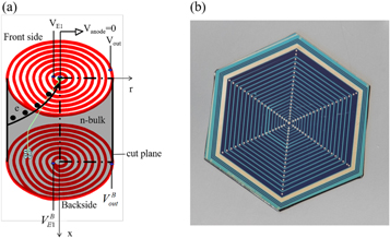
Figure 1. (a) Structure and principle diagram; (b) Picture of a 314 mm2 double-sided spiral SDD.
Download figure:
Standard image High-resolution imageThe present work focuses on analyzing the electrical characteristics of a 314 mm2 double-sided spiral SDD. The SILVACO TCAD semiconductor device simulator was used to simulate the electric potential, electric field and electron concentration of the detector. Also, the single event transient effect in the detector is studied by TCAD simulation. We analyzed the detailed electric field, the best electron drift channel, and charge collection of a 314 mm2 double-sided spiral SDD. In addition, the leakage current and capacitance of the detector were also measured. These analyses will aid in optimizing the structure design and improving the process of the detector.
2. Device structure and TCAD simulation
For the simulation of a 314 mm2 double-sided spiral SDD, SILVACO software had been utilized. It is almost impossible to conduct a full 3D simulation on a 314 mm2 double-sided spiral SDD due to the limit of computation capability of existing simulation software (due to the sheer size of the detector structure). For the analysis of our work, we thus undertook two-dimensional (2D) simulation. Figure 2 represents a 2D cross-section of a 314 mm2 double-sided spiral SDD structure used in the present simulation work, which obtained by making a cut plane in figure 1(a). The spiral cathode rings, with the doping concentration of 1 × 1018 cm−3 and doping depth of 1 μm, are all of the same type (p-type here), which are the opposite type to that of the substrate (n-type here, with a doping concentration of 6 × 1011 cm−3). The n+ anode with a doping concentration of 1 × 1019 cm−3 and a doping depth of 1 μm formed the center of the front side of the detector. The front and backside of the detector are covered by uniform silicon dioxide layers. The silicon dioxide on the n-type heavily doped layer is etched away and covered with a layer of aluminum to make contact electrodes. A small hole of 1 μm deep was etched on the outermost and innermost silicon dioxide layers of the spiral rings and then covered with an aluminum layer of the same thickness as the voltage input point. When appropriate reverse bias voltages VE1, Vout
, 
 are applied to the ohmic contact, the 314 mm2 double-sided spiral SDD will be depleted fully. Where VE1 and Vout
are the innermost and outermost voltage input points on the front side of the detector, and
are applied to the ohmic contact, the 314 mm2 double-sided spiral SDD will be depleted fully. Where VE1 and Vout
are the innermost and outermost voltage input points on the front side of the detector, and 
 are the innermost and outermost voltage input points on the backside of the detector. When the x-ray enters the reversed-biased detector, electron-hole pairs are produced in the detector depletion region. Electrons will drift to the anode along the electron drift channel, and the collected charge at the anode will generate an electric signal.
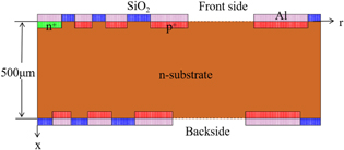
Figure 2. A 2D cross-section of a 314 mm2 double-sided spiral SDD.
Download figure:
Standard image High-resolution image3. Result analysis
3.1. E-potential, E-field and electron concentration distribution
In this section, 2D simulations are performed with Atlas to investigate the electric potential, electric field and electron concentration to explore the carriers drift behavior in the 314 mm2 double-sided spiral SDD. Figure 3 shows a 2D electric potential distribution in the 314 mm2 double-sided spiral SDD. It can be seen that the electric potential inside the detector is relatively uniform. As the radius increases, the electric potential gradually decreases. Also, the equipotential lines are displayed, so we can predict there is a possible drift path. Electrons will drift along the drift channel to the collecting anode.
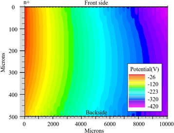
Figure 3. Electric potential distribution in a 314 mm2 double-sided spiral SDD.
Download figure:
Standard image High-resolution imageThe electric field distribution of a 314 mm2 double-sided spiral SDD is shown in figure 4. As can be seen, there is a low electric field region (on average of about 500 V cm−1) in the middle of the detector. The ionized electrons will gather in this region and drift to the anode. There is no zero E-field region in the detector, so it is completely depleted. There are some high electric field areas on the surfaces of the detector, so the intrinsic breakdown caused by a high electric field should be avoided in the design.

Figure 4. Electric field distribution of a 314 mm2 double-sided spiral SDD.
Download figure:
Standard image High-resolution imageFigure 5 reveals the electron concentration distribution of a 314 mm2 double-sided spiral SDD. It is obvious that the middle area of the detector has a high electron concentration zone. Still, the concentration is less than the substrate doping concentration, indicating that the substrate has been completely depleted. This area is the optimum electron drift channel. Electrons outside this region drift towards this region and the collecting anode.
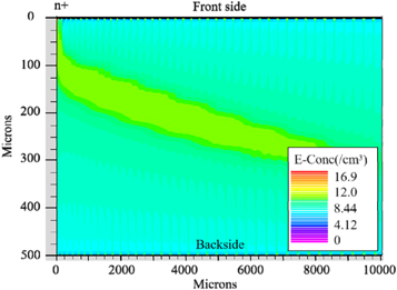
Figure 5. Electron concentration distribution of a 314 mm2 double-sided spiral SDD.
Download figure:
Standard image High-resolution imageAfter the above analysis, it shows that there is indeed the best drift electric field and optimum electron drift channel in the 314 mm2 double-sided spiral SDD, which verifies that the detector structure we designed using [5] is entirely reasonable. With the structural design and TCAD simulation, we developed a large-area SDD with an area of 314 mm2 at the initial stage, which made full preparation for the later manufacture of an ultra-large-area (≥400 mm2, diameter ϕ ≥ 20 mm) for detecting x-rays with energy between 600 eV and 20 keV.
3.2. Single event transient effect
Single event transient (SET) effect refers to the instantaneous fluctuation of current and voltage caused by incident particles, which is one of the essential subclasses of the single event effect (SEE). SEE is caused by a single heavy ion incident or passing through the electronic device, which is an important factor affecting the reliability of electronic devices. Therefore, in this part, the SET effect of the device is simulated, and then the transient current generation and charge collection are studied. The simulated heavy ion trajectory is incident vertically from the back of the detector, passing through the whole detector and emitting from the front side. The radius of the incident trajectory is 0.1 μm.
The peak value and pulse width of the current generated by the particle vary with the incident position. This is because the proportion of the charge obtained by drift and diffusion is different in the total collected charge for different incident positions. Figure 6 shows the trend of the transient current incident at different locations. It is obvious that the peak current and pulse width are larger when the energetic particles are incident on the anode, which is caused by the strong drift effect. On the contrary, when the particles are incident to other positions, the diffusion current plays a major role, and the current trends to be weak. By integrating the current transient waveform with time, the collected charge can be obtained.

Figure 6. Transient current at different incident positions, LET = 0.2 pC μm−1.
Download figure:
Standard image High-resolution imageThe transient current changes with time at different LET values are shown in figure 7. Obviously, the greater the value of LET, the greater the peak current. However, the shape of the current curve corresponding to different LET values is consistent. The current increases rapidly when the particles begin to enter, which is caused by the increase in the number of electron-hole pairs generated on the trajectory of the incident particles, and the larger the LET value, the more electron-hole pairs generated. These electron holes generate a sharply rising current for a part of them collected by the anode. Subsequently, the current began to decrease slowly due to carrier diffusion.
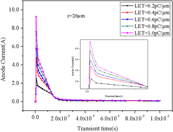
Figure 7. Transient current at different LET values.
Download figure:
Standard image High-resolution image3.3. Current-voltage (I-V) and capacitance-voltage (C-V) characteristics
The I-V and C-V characteristics of the 314 mm2 double-sided spiral SDD were measured at the room temperature. Figure 8 shows the test results of the leakage current of the detector. From figure 8, although the anode leakage current is very small for the detector with such a large area, we must improve and optimize the design in order to achieve the world's leading index parameters (leakage current less than 40 nA). Figure 9 represents the capacitance of the 314 mm2 double-sided spiral SDD. It can be seen from the figure 9 that the capacitance of detector is about 7 pF. To achieve the ideal value of capacitance (capacitance is less than 100 fF), structure optimization is essential. In addition, it is necessary to improve the process when making the detector.
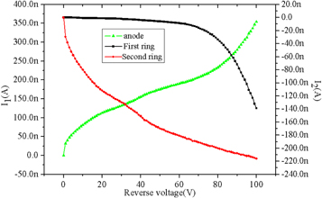
Figure 8. Leakage current of the 314 mm2 double-sided spiral SDD.
Download figure:
Standard image High-resolution image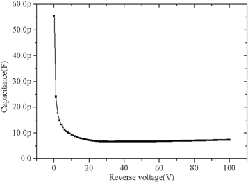
Figure 9. Capacitance of the 314 mm2 double-sided spiral SDD.
Download figure:
Standard image High-resolution image
Developing a detector is a difficult task, and it is a very long process. However, we are lucky to design and manufacture a 314 mm2 double-sided spiral SDD. After simulation and experimental analysis, although some of the data is not perfect, it gives us confidence and the idea of continuous improvement and optimization. This is worthy of recognition. We will improve the shortcomings of the detector and strive to achieve the best advantages.
4. Conclusions
In this work, we studied the electrical characteristics of a 314 mm2 double-sided spiral SDD. By simulating the electric potential, electric field and electron concentration distribution, the best drift electric field and the optimal electron drift channel of the detector can be determined. When x-ray enters the detector, electrons produced by ionization will drift to the collecting anode along the electron drift channel, and finally, be amplified and read out to realize the purpose of detecting x-ray. Also, we carried out the single event transient effect simulations for the 314 mm2 double-sided spiral SDD. It can be seen from the simulation results that the current increases rapidly at first and then decreases slowly when the heavy ions are incident. At the same time, the transient current is affected by the position of a particle incident. Moreover, the larger the LET value of the incident particles, the larger the pulse peak and pulse width of the transient current. Finally, we measured the leakage current and capacitance of the detector at room temperature and the results were relatively satisfactory.
The carrier drift behavior, single event effect, I-V and C-V characteristics of the detector are obtained through simulation and experimental analysis, which provides a theoretical basis for the structure design, carrier behavior research and single event effect test method of ultra large area detector, and also provides theoretical support for the anti radiation reinforcement design of the detector.
Acknowledgments
The authors would like to thank the financial supports from the Key Project of National Natural Science Foundation of China under Grant No. 11835008, the National Key R&D Program of China under Grant No. 2017YFF0105000, and the Special Project of Changsha-Zhuzhou-Xiangtan National Independent Innovation Demonstration Area under Grant Nos. 2017GK2293 and 2018XK2303.