
Abstract
Microwave absorbers have been attracted much more attentions in both military and civil fields nowadays. In this paper, we present a multi-band metamaterial absorber with the excellent performances of wide-angle incidence and polarization insensitivity. The designed absorber is composed of two distinct metallic layers separated by a dielectric substrate. The simulated absorptions of the absorber are 92.9%, 92.5% and 98.5% at 5.92 GHz, 6.12 GHz and 8.54 GHz, respectively. The microwave experiments are performed to verify the simulations, and the measured results are in agreement with the simulations. Surface current distribution is illustrated to investigate the physics of absorption. We believe that the designed absorber has numerous potential applications in stealth, sensing, electromagnetic absorption and thermal detectors.
Export citation and abstract BibTeX RIS

Original content from this work may be used under the terms of the Creative Commons Attribution 4.0 licence. Any further distribution of this work must maintain attribution to the author(s) and the title of the work, journal citation and DOI.
1. Introduction
Electromagnetic (EM) metamaterials (MMs) are artificial structures consisting of periodic array, which can demonstrate the unique physical phenomena when EM wave interact with the matters, and these unique physical phenomena is usually not existed in natural materials, For example, EM cloaks [1], perfect lens [2], energy harvesting [3, 4], perfect absorbers [5–13] et al Since the first perfect MM-based absorber (MMA) was designed and fabricated [5], MMAs have increasingly attract researchers due to their various applications including RCS reduction, sensors and wireless energy transfer [14–16]. In the last decades, researchers have introduced various absorbers working on different frequency band, ranging from radio waves to optical light [17–25]. In the meantime, the bandwidth of the MMAs has gradually expanded from the single band, multi-band to broadband, and even to the ultra-broadband. Several conventional approaches have been proposed to achieve multi-band and broadband absorption. Wang et al presented a five-band terahertz absorber by assembling three nested split-ring resonators (SRRs) with slightly different sizes [26]. Kim et al [27] proposed an ultra-broadband [28–35] absorber based on multi-layers. Moreover, Cheng et al [36] greatly enhanced the bandwidth of a broadband MA by loading lumped resistors. In general, MAs often have one metallic film on the bottom, which means no transmission wave. Therefore, it is simpler for MAs to be manipulated to achieve multi-band and broadband absorber. However, the metallic film on the bottom limits the application of the MA. Instead, a partly covered MA with a patterned metallic layer on the bottom is beneficial to save material, and it is possible that a good design of the structure lead to low transmission.
These absorbers conventionally consist of patterned metal and planar dielectric substrates, and the transmission is zero because of the metallic ground plane. Considering the limitation that planar MAs are often too hard to bend, some are flexible and can be bent easily, resulting in their great adaption to reality [37].
In this paper, we present a triple-band MA with C4 symmetric structure, ensuring the polarization independence. Although the bottom layer is a patterned structure which does not completely cover the substrate, the transmission can still be very low. The absorption peaks are nearly perfect in the microwave spectral. Therefore, the MA will be broadly applied in stealth, sensing, perfect absorbers, and thermal detectors.
2. Design, simulation and experiment
Figure 1 shows the structure of the designed MA, which is composed of two different metallic layers and a FR-4 substrate with thicknesses of 0.035 mm and 1.6 mm, respectively. The metallic layers are pure copper with the electric conductivity of σ = 5.96 × 10⁷ S m−1. The loss tangent and dielectric constant of the FR-4 are 0.025 and 4.3, respectively. The top layer structure is shown in figure 1(a), where the electric ring resonator (ERR) is rotated by 90° to form the symmetrical structure. The closed square loops (CSL) with different lengths are etched on the bottom layer as shown in figure 2(b), and the absorption is unchanged under different polarization angles because of the symmetry. The geometric parameters of the structure are h = 1.6 mm, t = 0.035 mm, a = 20 mm, x = 8.5 mm, y = 9.6 mm, w = 1.4 mm, r = 1.6 mm, d = 2 mm, g = 0.73 mm, s = 8.8 mm, n = 0.4 mm, k = 0.69 mm.
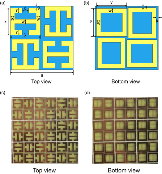
Figure 1. The designed absorber (a) and (c) top view and (b) bottom view, and a part of picture of the fabricated sample (c) top view, (d) bottom view.
Download figure:
Standard image High-resolution image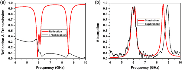
Figure 2. (a) Simulated results of reflection and transmission; (b) simulated and measured results of absorption.
Download figure:
Standard image High-resolution imageThe simulation is performed by CST Microwave Studio, with periodic boundaries in x and y direction, and an open-add-space boundary applied in z direction. The parameters are optimized to achieve multiple high absorption. The absorption is calculated by  where S11 and S21 are the reflection and transmission, respectively. For the experiment, the samples with the same geometry of the simulations are fabricated using a printed circuit board process, with overall dimension 20 × 20 cm2, which is shown in figures 1(c) and (d). Two horn antennas are both connected to the vector network analyzer, Agilent Technologies E8362B. One of the antennas emits the EM wave and the other one is a receiver. The scatter parameters of S21 and S11 can be obtained by setting the antennas on different sides and the same side with the sample respectively.
3. Results and discussions
The simulated results of reflection and transmission are shown in figure 2(a). We can see that the reflection amplitude is 0.08, 0.24, and 0.09 at the frequencies of 5.92, 6.12, 8.54 GHz, respectively, and the transmission amplitude is 0.25, 0.12, and 0.08 at the frequencies of 5.92, 6.12, 8.54 GHz. Moreover, the transmission amplitude reduces sharply from 5.78 GHz to 6.16 GHz and remains under 0.1 from 6.16 GHz to 10.0 GHz. The absorptions are 0.93, 0.93, 0.99 at the frequencies of 5.92, 6.12, 8.54 GHz, respectively, which is depicted in figure 2(b). The full width at half maximum (FWHM) bandwidth is 0.49 GHz within a center frequency of 6.0 GHz. It can be concluded that the three high absorption peaks are attributed to the decrease of reflection and transmission simultaneously.
The measured absorption agrees well with the simulation. All of the three absorption bands are successfully measured, which are 0.92, 0.95 and 0.96 of 5.92, 6.06 and 8.90 GHz, respectively. However, the third absorption frequency is higher than the simulated one. We conjecture that the dielectric constant has a slight difference between the measured and the simulation. In addition, some edge diffractions are excited among the results because the size of the sample is not infinite, inconsistent with the periodic boundary conditions set in CST Microwave Studio.
To better understand the physics of absorption, we analyzed the surface current on top and bottom layer at 5.92, 6.12, 8.54 GHz under TE mode, as shown in figure 3. Apparently, the distribution of surface current in figures 3(a) and (b) is approximately the same on account of the absorption frequencies are very close (5.92 and 6.12 GHz). The surface currents are almost uniformly distributed in the upper ERR and ERR, the direction of the main current distribution is flowing upwards, which means that the electromagnetic absorption at these two frequencies is mainly caused by electrical resonance. However, the surface current at 8.54 GHz is mostly distributed in the cross-diagonal ERRs and the cross-diagonal CSLs shown in figure 3(c). The direction of the current in the front and back layers is in opposite, thus it means that the electromagnetic absorption at 8.54 GHz is caused by magnetic resonance.

Figure 3. Surface current distributions at resonant frequencies (a) 5.92, (b) 6.12, and (c) 8.54 GHz under TE mode.
Download figure:
Standard image High-resolution imageIn what follows, the performance of wide-angle incidence is discussed. Figure 4(a) refers to the simulated results for TE incident wave, and when θ ≤ 45° we can see that our proposed MA is independent of the incident angles θ, though the absorption rates drop and the third resonance frequency shifts to higher spectrum. Experimental results are consistent with simulation ones in figure 4(b). Interestingly, the four curves are very close, which means the absorption peaks and rates remain stable as θ changes. The variations of the FWHM bandwidth and the center absorption frequency in relation to the incident angle θ are shown in figure 4(c). The FWHM bandwidth decreases from 0.49 GHz to 0.35 GHz, while the absorption frequency varies a little less than 6.00 GHz. In addition, the third absorption drops moderately and the frequency grows slowly, as θ rises from figure 4(d). That is, the frequency of 8.54, 8.62, 8.80, 9.05 GHz for θ = 0°, 15°, 30° and 45° with the absorptions of 98.5%, 97.2%, 93.5% and 84.9%, respectively. Though the absorption when θ = 45° is not as high as that when θ = 0°, the MA still maintains great absorptions under oblique incidence.

Figure 4. Absorption under different incident angles for TE wave. (a) Simulated results, (b) experimental results, (c) variations of the FWHM bandwidth and the center absorption frequency, and (d) variations of the third absorption and the frequency.
Download figure:
Standard image High-resolution imageFor TM incident wave, the simulated results are shown in figure 5(a). We can conclude that the proposed MA is also unrelated to the incident angle θ about 0° to 45°. The measured results depicted in figure 5(b) reveal the insensitivity of θ very well and the same decrease trend of the third resonance frequency as the simulated results. The intense fluctuations below half absorbing are influenced by environmental noise and can be tolerable. As figure 5(c) shows, both the FWHM bandwidth and the center absorption frequency remain stable at 0.49 GHz and 6.00 GHz, respectively. The third frequency does not increase but decrease from 8.54 GHz to 7.67 GHz as θ increases in figure 5(d). The absorption remains higher than 90%, despite a slight drop from 98.5% to 91.4% when θ rises.
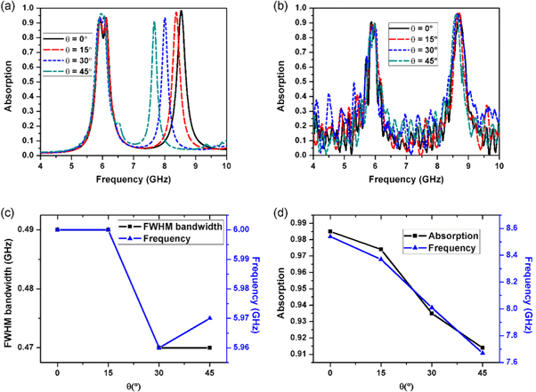
Figure 5. Absorption under different incident angles for TM mode. (a) Simulated results, (b) Experimental results, (c) variations of the FWHM bandwidth and the center absorption frequency, and (d) variations of the third absorption and the frequency.
Download figure:
Standard image High-resolution imageWe also demonstrate the parameter optimization on the designed absorber. Figure 6(a) illustrates the simulated absorption spectra when the gap of the top layer d oscillates around the initial value of 2.0 mm. Obviously, all the absorption peaks shift to higher frequencies as d increases and the absorption first increases and then decreases. The FWHM bandwidth follows an approximate pattern of growing and the center frequency also reaches its maximum at 6.27 GHz. Moreover, the dependence of the third absorption and frequency on d is shown in figure 6(c). The specific frequencies are 8.24, 8.38, 8.54, 8.62 and 8.70 GHz, when d changing from 1.0 to 3.0 mm with the step width 0.5 mm. Simultaneously, the absorption slightly drops in turn, but even the lowest is over 95%.
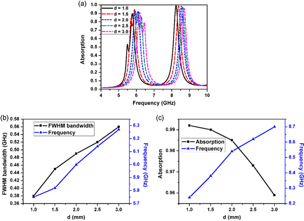
Figure 6. (a) Absorption with different gap of the EER (b) FWHM bandwidth and the center absorption frequency, and (c) variations of the third absorption and the frequency in relation to the gap width d.
Download figure:
Standard image High-resolution imageThe thickness of the FR-4 substrate h is also optimized to enhance the absorption. In order to make the figure of simulated results be seen more clearly, we split it into two parts, figures 7(a) and (b), showing at 4–7 GHz and 7–10 GHz, respectively. In figure 7(c), the FWHM bandwidth increases continuously from 0.33 GHz to 0.52 GHz as h rises, while the center absorption frequency fluctuates a little. In figure 7(d), the growth of h leads to the reduction of the third absorption frequency. However, at the meantime, the absorptivity sees an increase despite a slight decrease in the end. The minimum absorptivity is 90.2% at 9.40 GHz when h = 0.8 mm, while the maximum one is 98.5% at 8.54 GHz when h = 1.6 mm. Taking all factors into consideration, our absorber is optimized to the best according to the discussion of h.

Figure 7. The (a) Simulated results at 4–7 GHz, (b) simulated results at 7–10 GHz, (c) variations of the FWHM bandwidth and the center absorption frequency, and (d) variations of the third absorption and the frequency in relation to the thickness h.
Download figure:
Standard image High-resolution image
4. Conclusions
In conclusion, we design, fabricate and experiment a triple-band MA allowing both reflected and transmitted waves. The absorption is 92.9%, 92.5% and 98.5% of 5.92, 6.12 and 8.54 GHz, respectively, and the FWHM bandwidth is 0.49 GHz within a center frequency of 6.00 GHz. The MA is polarization insensitive due to its C4 symmetric structure. Additionally, the property of independence of wide incident angles is compatible both for TE and TM incident wave. The parameter d and h are optimized to achieve high absorption and multiple frequencies. The proposed MA will be applied to stealth, sensing, perfect absorbers, and thermal detectors.