
Abstract
Thin Film Transistors (TFTs) are the active elements for future large area electronic applications, in which low cost, low temperature processes and optical transparency are required. Zinc oxide (ZnO) thin film transistors (TFTs) on SiO2/n+-Si substrate are fabricated with the channel thicknesses ranging from 20 nm to 60 nm. It is found that both the performance and gate bias stress related instabilities of the ZnO TFTs fabricated were influenced by the thickness of ZnO active channel layer. The effective mobility was found to improve with increasing ZnO thickness by up to an order in magnitude within the thickness range investigated (20–60 nm). However, thinner films were found to exhibit greater stability in threshold voltage and turn-on voltage shifts with respect to both positive and negative gate bias stress. It was also observed that both the turn on voltage (Von) and the threshold voltage (VT) decrease with increasing channel thickness. Moreover, the variations in subthreshold slope (S) with ZnO thickness as well as variations in VT and Von suggest a possible dependence of trap states in the ZnO on the ZnO thickness. This is further correlated by the dependence of VT and Von instabilities with gate bias stress.
Export citation and abstract BibTeX RIS

Original content from this work may be used under the terms of the Creative Commons Attribution 3.0 licence. Any further distribution of this work must maintain attribution to the author(s) and the title of the work, journal citation and DOI.
1. Introduction
Poly-silicon thin film transistors (TFTs) have so far been the main attractive alternative to amorphous silicon TFTs used in large area electronic applications such as in flat panel displays [1, 2]. This has been due to the mobility limitation imposed on amorphous silicon based TFTs. However, both the poly silicon and amorphous silicon TFTs are non-transparent to visible light, thus would limit the aperture ratio of the active matrix arrays in flat panel displays. Semiconducting oxides with large bandgap (transparent to the visible regime, such as ZnO with a bandgap of ∼3.37 eV), can be used to fabricate high mobility TFTs (at temperatures lower than that used in poly silicon processes) and offer a way to overcome both the mobility and the transparency issues with improved device stability to light [3–10]. Transparent TFTs, based on ZnO have been demonstrated [1, 4, 5, 7]. These transistors exhibit high channel electron mobility that would lead to higher drive currents and faster device operating speeds (required for high frequency applications).
The source/drain (S/D) series resistance in field effect transistor (FET) devices is often determined as a sum of the source contact resistance (RS), the drain contact resistance (RD) and the channel resistance (Rch). As a consequence of the S/D contact resistance, current crowding in the source in the vicinity of the channel gives rise to the spreading resistance (Rsp). A first order approximation of Rsp is often given by the analytical expression (1);

where W is the channel width, ρ the source-drain resistivity,  the junction depth,
  the channel thickness and ξ is a scaling factor [11, 12]. In physical terms this means that both the doping concentration and the channel thickness can be used to modulate Rsp and hence the device performance. ZnO channel thickness has already been reported to be a useful parameter for modulating performance and off-state leakage currents in TFTs [13]. For TFT applications, the channel thickness (d) is related to off-state leakage current (Ids-off) when the gate to source voltage Vgs = 0 V, according to equation (2).

where σ is the electrical conductivity of the film, Vds is the source to drain voltage, W is the active channel width and L is the channel length.
Despite the advantages offered by ZnO TFTs, threshold voltage (VT) instability resulting from prolonged application of gate bias is one of the major challenges hindering its eventual integration into large area electronic technology [10, 14, 15]. The purpose of this work is to demonstrate that both performance and gate bias stress related electrical instability in ZnO TFTs can be modulated via thickness optimisation of the ZnO active layer.
2. Experimental
The effect of ZnO thickness on the performance of ZnO TFTs; and gate bias instability is demonstrated by sputtering ZnO layers of varying thicknesses (20–60 nm) on thermally grown silicon dioxide (SiO2) dielectric with identical deposition parameters. The relative dielectric constant of the SiO2 layer was obtained from capacitance-voltage (CV) data in the saturation region using the semiconductor parameter analyzers HP4192B by Agilent. The source/drain (S/D) electrodes are formed by depositing 100 nm aluminium patterned by shadow masks on the ZnO active channel length of 100 μm, and width/length ratio W/L = 10:1. The finished TFT is a bottom-gate (n+-silicon) inverted staggered configuration as in figure 1.
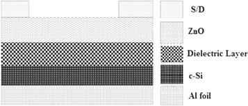
Figure 1. Inverted staggered bottom-gate TFT structure.
Download figure:
Standard image High-resolution imagePrior to sputtering the ZnO layer, a 100 nm layer of SiO2 was thermally grown in a Carbolite furnace at a temperature of 950 °C by the dry oxygen (O2) process. All the SiO2 layers used were grown at the same time in order to minimize any variations in the insulator thicknesses and properties. Different ZnO layers were then sputtered onto the SiO2 layer using a reactive RF magnetron sputtering process (O2/Ar ratio of 0.025) from a ceramic ZnO target of 99.99% purity. The ZnO layers were post-treated with O2 in vacuum (0.2 mTorr) for 30 min prior to breaking the vacuum to improve the film crystallites and its electrical stability in air [6]. The sputtering process was performed under room temperature conditions with no intentional heating. Film thicknesses were measured using a Rudolph AutoEL-III ellipsometer equipped with a 633.2 nm helium-neon (HeNe) laser at an incident angle of 70°. The thickness orders were confirmed by measurements obtained from surface profilometry using a Tencor Alpha Step 200 profilometer. The current-voltage (IV) characteristics were measured using an Agilent HP4140B pico ammeter. The stability of the devices were investigated under gate bias stress of ±10 V (corresponding to a field of 1 MV cm−1 for a 100 μm thick dielectric layer) for a maximum stress time of 104 s. All measurements were performed at room temperature in the dark.
3. Results and discussion
ZnO TFTs fabricated using the sputtered ZnO layers produced in this work exhibited the following characteristics (see table 1).
Table 1. Performance data of zno tfts across different ZnO thicknesses.
| ZnO thickness (nm) | μeff (cm2 V−1.s−1) | VT (V) | Von (V) | Ion-off | S (V dec−1) |
|---|---|---|---|---|---|
| 20 | 0.4 | 23.3 | 8.3 | 1.4 × 10⁷ | 1.4 |
| 25 | 2.0 | 22.7 | 2.0 | 1.2 × 10⁶ | 1.7 |
| 35 | 4.0 | 21.4 | 1.0 | 1.2 × 10⁷ | 0.9 |
| 40 | 7.0 | 18.7 | −4.5 | 1.6 × 10⁶ | 0.9 |
| 50 | 9.0 | 20.0 | −5.3 | 2.0 × 10⁵ | 2.5 |
| 60 | 10.9 | 18.5 | −9.1 | 5.1 × 10⁵ | 3.8 |
The threshold voltage (VT) and the effective mobility (μeff) were derived from a linear fit to a plot of drain current (Ids) versus gate to source voltage (Vgs) in the linear region with Vds = 2 V  according to the expression:

where  is the capacitance per unit area of the gate insulator, and W and L are the channel width and length respectively. The remaining parameters
 and
and  represent the permittivity in free space, the relative permittivity of SiO2 and the thickness of SiO2 respectively. In this work,
  was obtained from the CV measurement to be 3.9.
The turn-on voltage (Von) is extracted as the gate voltage at which the drain current just begins to increase monotonically with increasing gate voltage, and corresponds to the minimum current on the semi log plot of Ids versus Vgs. Using these parameters, the shifts Δμeff, ΔVT and ΔVon are calculated using the following relations (4a)–(4c).


where, 
 and
and  are the effective mobility, threshold voltage and turn-on voltages of the TFT after a stress bias time of t seconds respectively. The initial values of the parameters prior to the application of the gate bias stress correspond to
Typical output and transfer characteristics of the finished ZnO TFTs are shown in figures 2 and 3 respectively. In figure 3, a voltage sweep from −30 V to +30 V and back presents a hysteresis of about 1 V. This suggests the dielectric layer used is of good quality. From table 1, the subthreshold slope (S) for these devices ranges between 0.9 V/dec and 3.8 V/dec. The thickest film (60 nm) exhibited the largest value of S, which was more than double the value observed for the thinnest ZnO film (20 nm). The value of S is indicative of the trap density (Nt) at or near the interface between the ZnO semiconductor and gate dielectric material. Moreover, the variations in S with ZnO thickness as well as variations in VT and Von (see figures 6(b) and (c)) is an indication that interface traps may depend on the ZnO thickness. The total density of states present at all interfaces in the semiconductor  is estimated using equation (5) [16].

where k is the Boltzmann's constant, T is the measurement temperature, q the elemental electron charge, S the subthreshold slope, and Cins the capacitance of the dielectric layer.
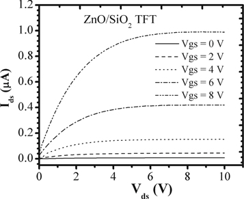
Figure 2. Typical output characteristic of a TFT incorporating a 40 nm thick active layer, clearly illustrating transistor action.
Download figure:
Standard image High-resolution image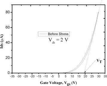
Figure 3. Typical voltage sweep transfer characteristic of a TFT incorporating a 40 nm thick active layer, indicating the threshold voltage.
Download figure:
Standard image High-resolution imageIt is also observed from table 1 that the thicker films presented superior performance with respect to the effective mobility even though a poorer subthreshold slope value is observed for the 50 nm film (the thickest). One may therefore speculate that traps states at the ZnO/insulator interface may not be responsible for the large values of S observed in thicker films. It is worth noting that all ZnO active layers used in this work were exposed to oxygen (O2) post-deposition treatment for 30 min prior to breaking the vacuum. Therefore the conductivities of the films at the top surface are modified by chemisorbed O2 [17, 18]. O2 chemisorption have been reported to degrade effective mobility in ZnO TFTs as well as shifting VT to more positive values [19]. On the average in this work, thinner films were observed to have larger values of VT. Although the effective mobility is observed to improve with film thickness. The effect of O2 chemisorption can be considered to be contant on all films as the post-deposition procedure was exactly the same for all films. One may therefore attribute the variations observed in VT and μeff to the dominance effect of the top surface due to O2 chemisorption on thinner films. As seen from table 1, Von values are more positive with decreasing ZnO layer thickness. This may be attributed to the fact that the negatively charged chemisorbed O2 species on the top surface deplete the ZnO layer of carriers during the adsorption process [18, 20]. The magnitude of the electric field created by these charged species at the ZnO/insulator interface is inversely proportional to the ZnO thickness. This is in agreement with thickness dependencies exhibited by the effective mobility as a result of reduced scattering from the electric field resulting from the chemisorption in thicker films.
One clearly sees from table 1 that within the thickness range studied, the effective channel mobility (μeff) exhibits a general increase with thickness (figure 4). This is similar to observations reported for undoped ZnO and other ZnO derivatives, hydrogenated amorphous silicon (a-Si:H) TFTs [21, 22]. In addition, turn-on voltage (VOn) and VT are observed to decrease monotonically with increasing thickness (figure 5). These relationships could be ascribed to a stronger effect of chemisorbed O2 [19] on the ZnO top surface with decreasing film thickness. All these will likely affect the performance of the TFT device.
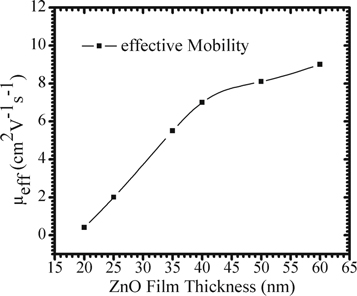
Figure 4. The variation of μeff with ZnO layer thickness.
Download figure:
Standard image High-resolution image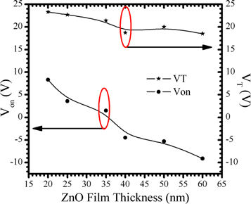
Figure 5. The variation of VT and Von with ZnO layer thickness.
Download figure:
Standard image High-resolution imageOn application of a +10 V or −10 V gate bias stress to the devices, it can be observed that the active layer thickness also affects the electrical stability of the ZnO TFT (figure 6). In general, it is observed that an application of a gate bias stress on the ZnO/SiO2 TFTs results in variations in μeff, VT and Von. An application of a positive gate bias stress moves the transfer characteristic curve to the right whereas a negative bias shifts the curve to the left (figure 7). Other authors have attributed such behaviours to charge trapping and detrapping at or near the semiconductor/dielectric interface as well as defects creation at longer stress times [19, 23, 24]. However, the fact that Ids-off is not enhanced by this instability suggest charge creation is not likely to be a significant effect. The shifts in Δμeff, ΔVT and ΔVon following a positive gate bias stress are shown in figure 7 for stresses up to a maximum of 104s. The gate bias stress was performed using stress time intervals of: 0, 101,102, 103 and 104 s. Similar behaviour has been reported in yttrium and tungsten doped ZnO TFTs and was dependent on doping concentration [25, 26]. We observed that the shifted characteristics curves returned freely to their original positions after relaxation time of 4 hours in air at room temperature following a 104 s stress time. This suggests that charge trapping at or near the interface in the semiconductor is the dominant mechanism responsible for the instability [27].
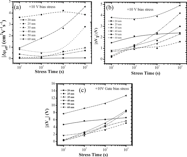
Figure 6. (a) Variation of effective mobility as a function of gate stress time parameterised for different ZnO thicknesses (20–60 nm). (b) Variations of threshold voltage as a function of gate stress bias time parameterised for different ZnO thicknesses (20–60 nm). (c) Variations of turn-on voltage as a function of gate bias stress time parameterised for different ZnO thicknesses (20–60 nm).
Download figure:
Standard image High-resolution image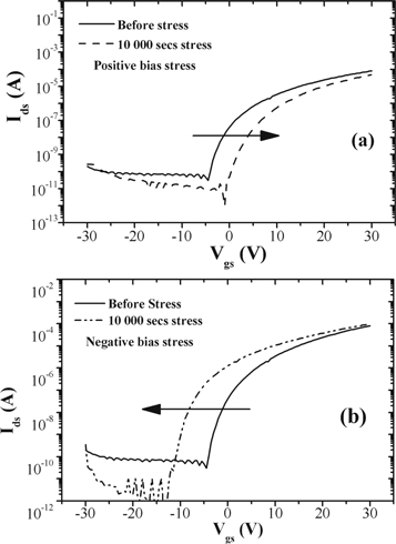
Figure 7. (a) Typical instability in SiO2 based ZnO TFT as a result of positive and negative bias stress showing the shift in the transfer characteristics following positive gate bias stress. (b) Typical instability in SiO2 based ZnO TFT as a result of positive and negative bias stress showing the shift in the transfer characteristics following negative gate bias stress.
Download figure:
Standard image High-resolution image
4. Conclusion
It has been shown that ZnO TFT performance parameters (μeff, VT and VOn) are affected by ZnO active layer thickness. It is suggested in this work that O2 adsorption at the ZnO top surface results in a carrier depletion that has a strong effect on the device performance. Also, the dependence of VT on channel thickness would lead one to speculate that TFTs optimised to operate at low VT are likely to be more stable during prolong operation. This can be attributed to reduced gate bias stressing effect at low operational voltages. It is also observed that for all three parameters (μeff, VT and VOn) studied in this work, greater instability as a result of gate bias stress is exhibit by thicker ZnO films.
Acknowledgments
This work was supported in part by the Faculty of Engineering and Technology of the University of Buea, Cameroon and De Montfort University, Leicester UK.