
Abstract
Uniform and well-adherent SnO2 thin films, with thickness ranging from 60 nm to 6 μm, were deposited on borosilicate glass substrate by Successive Ionic Layer Adsorption and Reaction (SILAR) technique. A micro-controlled SILAR unit was employed to precisely monitor the deposition conditions. The effect of precursor concentration and post-deposition annealing on the micro-structural and optical properties of SnO2 thin films were studied in detail. The films were found to possess tetragonal rutile structure. The crystallite size of the films increased with solution molarity. Microstructural properties were analyzed using Scherrer, Modified Scherrer, Williamsons-Hall and Size-Strain plot techniques. Different optical properties such as band gap, skin depth, extinction coefficient, Urbach energy etc were determined. The post-deposition annealing at a moderate temperature of 573 K was found to enhance the crystallite size of the films while the density of the defect energy states reduced.
Export citation and abstract BibTeX RIS

Original content from this work may be used under the terms of the Creative Commons Attribution 4.0 licence. Any further distribution of this work must maintain attribution to the author(s) and the title of the work, journal citation and DOI.
Introduction
In the past few decades, IV-VI group materials have been studied extensively due to their wide range of potential applications. Tin oxide (SnO2) is one of such earth abundant and nontoxic IV-VI material known for its transparency in visible region and a wide bandgap (3.5 to 4.0 eV) [1]. Due to its high absorption co-efficient in UV region and n-type conductivity, SnO2 has many potential applications such as gas sensors [2], window layers in solar cells, photodetectors [3–5] etc The SnO2 nano materials including thin films have been prepared by several physical and chemical routes such as chemical bath deposition [6], dip coating [7], sol-gel [8], thermal evaporation [9], Spray pyrolysis [10] pulsed laser deposition (PLD) [11], SILAR [12–14] etc Among these techniques, SILAR has proved to be a simple and cost-effective route for the synthesis of good quality SnO2 films as it does not require complex setups and vacuum environment [15]. Several efforts have been made in the past to synthesize SnO2 using SILAR and other techniques. However, the films obtained in most of these cases were amorphous and required a post-deposition heat treatment at high temperature to improve the crystallite size [16–18]. Besides, the SILAR deposition process in most of the published works has been manually controlled and hence the results are unreliable. The effect of deposition parameters on microstructural properties of SnO2 films has not been studied in-detail. In the present work, an attempt has been made to deposit SnO2 films on borosilicate glass substrates by an automated, microcontroller based SILAR unit without any complexing agents. The microstructural properties have been analyzed using four different methods. The effects of precursor concentration and annealing on the properties of the films have been investigated in detail.
Experimental details
The SnO2 thin films were deposited on borosilicate glass substrates (75 × 25 × 1.35 mm). Before deposition, the substrates were cleaned in 30% diluted HCl and acetone for 10 min each. The excess acids were removed by rinsing with double distilled water and finally the substrates were dried for 10 min in a hot air oven. The deposition was carried out in a micro-controlled SILAR coating unit (HOLMARC TM Opto-mechatronics, Kochi, INDIA). The aqueous solutions of SnCl2.2H2O and 1% H2O2 were used as cationic and anionic precursors respectively. The steps involved in the deposition process are described below.
At first, well cleaned substrates were immersed in cationic precursor containing 60 ml of SnCl2.2H2O of known molarity. The substrates were stirred at a steady rate to allow the adsorption of tin ions onto the substrate surface. The poorly adhered ions were rinsed off by immersing the substrates in double distilled water. Later, the substrates were immersed in anionic precursor which was prepared by dissolving 2 ml of 1% H2O2 in 60 ml double distilled water and rinsed as mentioned above. The chemical reactions are given below


This entire sequence represents one complete SILAR immersion cycle [19] (figure 1). The said cycle was repeated several times to get SnO2 films of desired thickness.

Figure 1. The SILAR process for the deposition of SnO2 films.
Download figure:
Standard image High-resolution imageIn any SILAR deposition, the properties of the end products are highly influenced by preparative parameters such as solution molarity, temperature of the solutions, no. of cycles, dip duration, etc In this work, the solution molarities of both cation and anions were varied from 0.00625 M to 0.05 M with an interval of 0.025 M. The number of immersion cycles was varied from 25 to 100 with an interval of 25 cycles. The dip duration was kept constant at 20 seconds. All the samples were prepared under room temperature (300 K) and pressure. After the deposition, the films were air annealed at moderate temperature of 573 K for one hour using a hot plate and gradually cooled. The as-deposited and air annealed samples were characterized by employing different techniques which are discussed in the next section.
Results and discussion
Thickness
The thickness of the films was measured gravimetrically and later verified by profilometer (Bruker Dektak XT). The thickness of the SnO2 films was found to increase with the number of immersion cycles and also with the solution molarity (figure 2). The films were found to be well adherent up to a thickness of 6 micrometers. However, when the thickness increased above 6 micrometer, the material of the films started to peel off from the surface due to insufficient adhesion. The maximum thickness limit of 6 micrometer was reached for a precursor concentration of 0.05 M after 100 immersion cycles.

Figure 2. The variation of film thickness with solution molarity and no. of cycles.
Download figure:
Standard image High-resolution imageStructural analysis
The XRD patterns of the SILAR deposited SnO2 thin films are shown in figures 3 and 4. The films obtained from higher concentrations of precursors showed distinct XRD peaks indicating better crystallinity. These relatively thicker films exhibit tetragonal rutile structure with prominent peaks corresponding to (110), (101), (200), (210) and (211) planes (JCPDS card no. 77-0450) [20]. The intensity of the (210) peak was found to be relatively higher than that previously reported by others [17, 18]. The observed peaks were relatively broad due to the nano-crystalline nature of the films. However, the post-deposition annealing was found to increase the crystallite size. Ali Yıldırım et al [13] and Yu et al [17] have reported a similar improvement in the crystallite size of SnO2 after annealing. The highest crystallite size reported in these two cases was about 20 nm. However, the annealing temperatures used in their work were much higher (673 K and 873 K respectively). Such high temperatures will produce stress in the films due to the difference in the thermal expansion coefficients of the substrates and SnO2. In the present work, we have been able to obtain the average crystallite size of about 25 nm (average value of crystallite size obtained from MDS and S-S plot techniques) at a much lower annealing temperature of 573 K. This crystallite size is five times higher than that reported by Shipra Raj et al after annealing SnO2 films at 573 K [21].
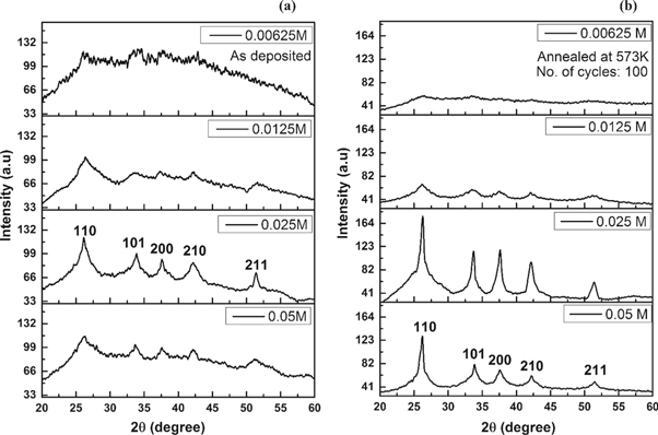
Figure 3. The XRD pattern of (a) as-deposited and (b) annealed samples at different solution molarities.
Download figure:
Standard image High-resolution image
Figure 4. The XRD pattern for (a) as-deposited and (b) annealed samples for obtained at different number of immersion cycles.
Download figure:
Standard image High-resolution imageThe crystallite size of materials is usually determined from Scherrer formula which makes use of the FWHM of the XRD peaks. However, the accuracy of this technique is limited in the case of nano-crystalline films due to the considerable peak broadening. Since the films are annealed, the effect of stress must be considered. Hence, in the present work we have used four different methods (namely Scherrer, Modified Debye–Scherrer, Williamsons-hall technique and size-strain plot) to characterize the microstructural properties of the films.
Scherrer technique
The crystallite size and strain in the films were determined from Scherrer equations as follows [22]


where λ is the x-ray wavelength, β is the full width of the peak at half maximum (FWHM), θ is the Bragg angle (in radian) and ε is the strain. The crystallite size of the films increased with thickness. The continuous increase in the crystallite size with thickness suggests that the newly adsorbed atoms in each SILAR cycles are predominantly joining the existing crystallites rather than forming new ones. The inherently slow deposition rate of SILAR makes it possible for the atoms to join the existing crystallites. The crystallite size was found to increase after annealing as well. The grain boundary region between the crystallites is characterized by lack of any periodic structure and hence a higher concentration of defects. When the film is annealed, the loosely held atoms in the grain boundary region receive thermal energy. The increased mobility of these atoms helps them to join the nearby crystallites and, as a consequence, the average crystallite size of the films increases.
The d-spacing, lattice constants were calculated for tetragonal structure using the relation,

Using Bragg's equation  in the above equation (with n = 1) we get,

The lattice constant 'a' was calculated from the relation:

The lattice constant 'c' was calculated by substituting 'a' as follows:

The standard values of lattice parameters are, a = b = 4.7382 Ao, c = 3.1871Ao, Volume V = 71.55 (AO)3, c/a = 0.6726 [20]. The observed values of d spacing and lattice parameters were slightly (2% to 5%) high compared to the standard value (table 1). The deviation from the standard values indicate the presence of stress. The lattice strains were found to decrease initially whereas c/a ratio remained almost constant (table 2). The internal stress and no. of crystallites per unit volume are tabulated in table 3.
Table 1. Variation of interplanar spacing with solution molarity and annealing (573 K).
| 0.0125 M, 100 Cycles (Thickness 0.345 μm) | 0.025 M, 100 Cycles (Thickness 1.86 μm) | 0.05 M, 100 Cycles (Thickness 6 μm) | ||||||||||||
|---|---|---|---|---|---|---|---|---|---|---|---|---|---|---|
| hkl values | Std. values JCPDS card no. 77-0450 | As deposited | Annealed | As deposited | Annealed | As deposited | Annealed | |||||||
| 2θ (Degree) | d (A°) | 2θ | d | 2θ | d | 2θ | d | 2θ | d | 2θ | d | 2Ѳ | d | |
| 110 | 26.61 | 3.35 | 26.48 | 3.36 | 26.22 | 3.39 | 26.22 | 3.39 | 26.28 | 3.38 | 26.14 | 3.40 | 26.24 | 3.39 |
| 101 | 33.89 | 2.64 | 33.5 | 2.67 | 33.66 | 2.65 | 33.86 | 2.64 | 33.72 | 2.65 | 33.84 | 2.64 | 33.88 | 2.64 |
| 200 | 37.95 | 2.37 | 37.32 | 2.40 | 37.74 | 2.38 | 37.56 | 2.39 | 37.64 | 2.38 | 37.76 | 2.37 | 37.6 | 2.38 |
| 210 | 42.64 | 2.12 | 42.2 | 2.13 | 42.28 | 2.13 | 42.26 | 2.13 | 42.18 | 2.13 | 42.22 | 2.13 | 42.24 | 2.13 |
| 211 | 51.78 | 1.79 | 51.48 | 1.77 | 51.44 | 1.77 | 51.46 | 1.77 | 51.4 | 1.77 | 51.32 | 1.78 | 51.52 | 1.77 |
Table 2. Variation of lattice constants and cell volume with solution molarity and annealing.
| Parameters | a(A°) | Δa | c | Δc | Δa/ao | Δc/co | V(Ao)3 | c/a |
|---|---|---|---|---|---|---|---|---|
| Standard | 4.74 | --- | 3.18 | --- | --- | --- | 71.55 | 0.67 |
| Calculated | 4.79 | 0.05 | 3.07 | 0.12 | 0.01 | 0.04 | 70.25 | 0.64 |
Table 3. The microstructural properties calculated using Scherrer, Modified Debye–Scherrer, Williamsons-Hall and Size-Strain plot (SSP) techniques.
| Scherrer technique | Modified Debye–Scherrer | Williamsons-Hall | Size-Strain plot | ||||||||||||
|---|---|---|---|---|---|---|---|---|---|---|---|---|---|---|---|
| Condition | Precursor Concentration (M) | D size (nm) | Strain ε X 10−3 | Stress (Gpa) | N ( X 1018 ) | D size (nm) | N (X 1018 ) | D size (nm) | Strain ε X 10−3 | Stress (Gpa) | N (X 1018 ) | D size (nm) | Strain ε X 10−3 | Stress (Gpa) | N (X 1018 ) |
| As deposited | 0.0125 | 2.84 | 52.9 | 3.06 | 15.06 | 3.75 | 6.54 | 2.47 | 78.74 | 19.92 | 22.89 | 2.56 | 58.96 | 14.91 | 20.56 |
| 0.025 | 7.74 | 25.02 | 1.43 | 4.01 | 5.28 | 12.63 | 4.42 | 37.92 | 9.59 | 21.54 | 5.6 | 23.19 | 5.86 | 10.59 | |
| 0.05 | 3.19 | 50.06 | 2.89 | 184.83 | 4.32 | 74.42 | 2.57 | 87.06 | 22.02 | 353.46 | 2.7 | 54.86 | 13.87 | 304.83 | |
| Annealed (573 K) | 0.0125 | 4.11 | 39.54 | 2.26 | 4.96 | 4.46 | 3.88 | 3.88 | 17.19 | 4.34 | 5.90 | 3.54 | 37.41 | 9.46 | 7.77 |
| 0.025 | 13.49 | 8.28 | 0.46 | 0.75 | 28.18 | 0.08 | 55.87 | 36.08 | 9.12 | 0.01 | 20.91 | 11.83 | 2.99 | 0.20 | |
| 0.05 | 11.90 | 9.71 | 0.55 | 3.56 | 20.06 | 0.74 | 84.15 | 42.4 | 10.72 | 0.01 | 14.60 | 13.78 | 3.48 | 1.92 | |
Modified Debye–Scherrer (MDS) technique
The modified Scherrer formula determines the average value of crystallite size D by considering the least square fit over all the diffraction peaks.
From equation (1), we have,

taking logarithm on both sides,

The plot of lnβ v/s ln(1/cos θ) gives a straight line with negative y -intercept (figure 5(a)). The exponential of the y-intercept was used for the calculation of average crystallite size [23] (table 3). The MDS technique determines the average crystallite size considering multiple peaks in the XRD patterns. The values are therefore different from those obtained by simple Scherer formula. The main limitation of MDS technique is that the micro strain cannot be calculated.
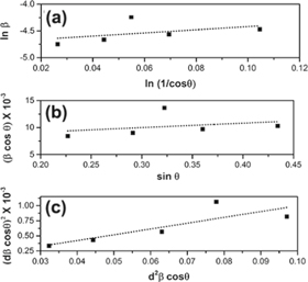
Figure 5. The typical (a) Modified Debye–Scherrer, (b) Williamson-Hall and (c) size-strain plots of SnO2 films (0.05 M, 100 cycles, 573 K).
Download figure:
Standard image High-resolution imageWilliamsons-Hall technique
The Williamsons -Hall technique provides a better estimation of the crystallite size under the influence of micro strain. The method considers the micro strain and the broadening of the XRD peaks assuming an uniform distribution of strain in all crystallographic planes (UDM model). The strain-induced broadening is given by the equation,

Where 4εtanθ gives the strain-induced broadening. Multiplying both sides with cosθ, the equation takes the form,

In the ideal case, a plot of βcosθ v/s 4sinθ will be a straight line whose slope gives us the values of micro strain and Y-intercept gives the average crystallite size. The plot of βcosθ v/s 4sinθ for SnO2 films are showed in figure 5(b). The scattering of data points indicates the inhomogeneous distribution of strain within the films [24, 25]. After annealing, the micro strain and stress decreased linearly. The no. of crystallites per unit volume determined from W-H method are given in table 3. The values of average crystallite size determined by W-H method deviated from those obtained by Scherrer formula and Modified Scherrer methods. This deviation arised mainly because of the fact that W-H equation assumes uniform distribution of strain which may not be applicable in the present case.
Size-Strain (S-S) plot technique
The size-strain plot technique makes use of the following equation for the calculation of crystallite size and micro strain:

The variation of (dβcosθ)2 vs (d2 βcosθ) is shown in the figure 5(c). The crystallite size is estimated from the slope of the graph (table 3). The obtained crystallite size was found to be in good agreement with that obtained from modified Scherrer technique. The maximum crystallite size 21 nm was obtained for solution molarity of 0.025 M (100 cycles) which was annealed at 573 K.
The strain in the films was found to vary inversely with the crystallite size. One of the main reasons for the development of strain is the imperfections in the crystal structure. When the average crystallite size is low, the crystal structure of the film has more imperfections which leads to the development of strain. When the crystallite size increases the strain reduces.
The original Scherrer equation calculates crystallite size and strain by considering only one peak which has the maximum intensity. It is well known that, Scherer equation only makes use of the full width at half maximum (FWHM) of the peak to find the crystallite size. However, in polycrystalline films (such as SnO2 in the present case), an additional peak broadening may occur due to stress. This factor is not considered in the original Scherrer equation. Hence the crystallite size obtained from Scherrer equation is usually less than the actual crystallite size.
Unlike the original Scherrer equation, the modified Scherrer equation calculates average crystallite size by considering more than one peak. Hence the modified Scherrer equation (MDS), provides more accurate values of crystallite sizes than the simple Scherrer equation. However, it is not efficient enough to deduce the influence of micro-strain and the resultant broadening of the XRD peaks.
The William-Hall equation determines crystallite size and strain by using multiple diffraction lines. The values obtained by W-H method are more accurate compared to Scherrer and MDS equations. However, the W-H model assumes uniform distribution of strain which is not perfectly suitable in the present case. The S-S plot technique, on the other hand, does not assume uniform distribution of strain and hence can be used for polycrystalline films as well. Besides, the S-S plot technique estimates the impact of micro-strain by considering lattice spacing (d-spacing), which has the advantage that less weightage is given to reflections at high angles, where the precision is usually lower. Among different techniques, size-strain plot is therefore found to be the most appropriate method in the present case.
The SEM images of the films (figure 6) indicated a uniform substrate coverage of the film material despite the inhomogeneous distribution of stress. Even after annealing, the films remained intact and no deformities (such as cracks) were observed on the film surface.
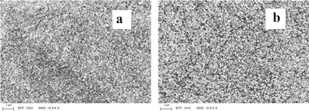
Figure 6. The typical SEM images of the (a) as-deposited and (b) annealed samples (0.025 M, 100 cycles).
Download figure:
Standard image High-resolution imageThe composition of the films was ascertained by EDAX analysis (table 4). The films were found to have almost stoichiometric composition (figure 7). During the EDAX analysis, the x-rays penetrate very thin films and reach the glass substrate. Hence a small excess of oxygen was observed in the EDAX data of very thin films. This excess oxygen content is actually coming from the borosilicate glass substrate and not from the SnO2 films. This claim is supported by the fact that the thicker (6 micron) SnO2 films show nearly perfect stoichiometry without any oxidation. In case of thicker films, the amount of x-rays reaching the glass substrate is very less. Hence the oxygen content found in their EDAX data comes almost entirely from the films.
Table 4. The Sn:O ratio of as-deposited and annealed SnO2 films.
| Condition | Precursor concentration (M) | Sn:O ratio (determined from EDAX) |
|---|---|---|
| As deposited | 0.0125 | 0.47 |
| 0.025 | 0.48 | |
| 0.05 | 0.49 | |
| Annealed (573 K) | 0.0125 | 0.47 |
| 0.025 | 0.47 | |
| 0.05 | 0.49 |
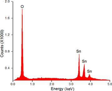
Figure 7. The typical EDAX spectra of SnO2 films.
Download figure:
Standard image High-resolution imageOptical properties
The optical absorbance spectra of as-deposited and annealed SnO2 films are shown in figures 8(a) and (b). The films showed high optical absorption in the wavelength range of 300 to 400 nm. A gradual increase in optical absorbance was observed at longer wavelengths for low concentration but for the films of 0.05 M concentration the absorption was relatively high throughout the wavelength range (300–1100 nm). The 6 μm thickness was the main cause for the high absorption. No significant change was observed in the absorption spectra upon annealing. The relation between the absorption coefficient α and optical energy band gap can be written as;

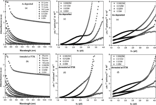
Figure 8. The absorbance spectra of (a) as-deposited and (b) annealed samples along with the respective Tauc plots (c) to (f).
Download figure:
Standard image High-resolution imageIn the above equation, A and n are constants. Here, n can have different values corresponding to the transition mode. The Tauc plots  were drawn (figures 7(c)–(f)) with n = 2 (for direct transition) and n = 1/2 (for indirect transition). The linear portion of the curves were extrapolated to calculate the direct and indirect band gaps. As the solution concentration increased, the direct bandgap of both as-deposied and annealed films decreased from 3.36 eV to 2.26 eV while the indirect bandgap changed from 3.04 eV to 1.61 eV. The increase in the crystallite size can be attributed for bandgap reduction. The optical absorption of SnO2 layers can be characterized with the help of extinction coefficient, skin depth (penetration depth) and Urbach energy. The skin depth (δ) is an optical characteristic of any film which can quantify the reduction in photon density by a factor 'e' after crossing a layer of certain thickness. In the present case, it was determined by the relation [26] ;

The penetration depth was found to be maximum for the films obtained from 0.025 M precursors (100 cycles). However, the penetration depth remained almost constant and reduced at longer wavelength region for the same concentration upon annealing. Also, further increase in the molarity reduced the penetration depth (figure 9(a)). The extinction coefficient which quantifies the absorption loss that happens within the SnO2 films when illuminated was determined by;


Figure 9. The variation of (a) skin depth (b) extinction coefficient and (c) Urbach energy in as-deposited and annealed samples.
Download figure:
Standard image High-resolution image
The extinction co-efficient was found to be maximum for lower concentration but decreased as the solution molarity increased due to the tendency of relatively thicker films to absorb more photon energy (figure 9(b)). The values of optical parameters are tabulated in table 5.
Table 5. Optical parameters of as-deposited and annealed SnO2 films.
| Condition | Solution Molarity (M) | Band gap (eV) | Skin depth δ(cm) X 10−5 | Extinction Coefficient (k) | Urbach energy (eV) | |
|---|---|---|---|---|---|---|
| Direct | Indirect | |||||
| As deposited | 0.00625 | 3.36 | 3.04 | 0.14 | 0.07 | 2.17 |
| 0.0125 | 3.31 | 2.27 | 0.43 | 0.17 | 1.28 | |
| 0.025 | 3.25 | 1.79 | 2.23 | 0.05 | 0.95 | |
| 0.05 | 2.31 | 2.16 | 0.33 | 0.02 | 4.16 | |
| Annealed 573 K | 0.00625 | 2.97 | 2.85 | 0.16 | 0.21 | 1.84 |
| 0.0125 | 3.31 | 2.27 | 0.42 | 0.20 | 1.27 | |
| 0.025 | 3.13 | 1.61 | 1.93 | 0.05 | 0.86 | |
| 0.05 | 2.26 | 2.16 | 0.28 | 0.02 | 3.33 | |
The nano crystalline nature of the films often introduces defect energy levels within the bandgap. The Urbach energy (Eu ) is a measure of the amount of such disorderness. In the present case, the Urbach energy associated with the samples were calculated using the relation;

The figure 9(c) shows the typical Urbach tail. The reciprocal of the slope was used to determine the Urbach energy. The films obtained at 0.025 M concentration showed significant reduction in Urbach energy compared to other solution molarities. The Urbach energy was found to reduce after annealing at 573 K, which confirms the reduction in defect energy levels.
Conclusions
Uniform SnO2 thin films with various thickness were obtained from microcontroller based SILAR technique. The thicker films exhibited tetragonal rutile structure. The enhancement in the crystallite size and reduction in strain within the stoichiometric range was achieved by moderate air annealing. The microstructural properties were analyzed using four different techniques out of which size strain technique was found to be more reliable. A significant improvement in crystallite size was achieved at much at much lower annealing temperature than that employed by other authors. Both as-deposited and annealed films showed considerable absorption in the ultraviolet region. The Urbach energy of the films was found to reduce after the post-deposition annealing. The direct bandgap range of the films is ideal for applications such as UV-Visible photodetectors and window layers of solar cells.