
Abstract
We managed to produce truly transparent conductive monolayer graphene films using commercially available graphene nano-flakes by utilizing the Langmuir-Blodgett technique. The monolayer films could only be produced under specific solution concentration, sonication time, and evaporation conditions. The described method eliminates the need for intermediate processing steps, such as adding surfactant or annealing during the process. Film structure is characterized using scanning tunneling microscopy and high-resolution electron transmission microscopy. Mechanical characterization shows that the film exhibits a nonlinear stress-strain curve with a strain stiffening behavior in agreement with previous theoretical predictions. Film stiffness ranges between 40 and 80 MPa. The produced monolayer graphene films exhibit full transparency in the wavelength range of 400 nm to 1100 nm, and an excellent electrical conductivity ∼104 S cm−1 which is comparable to the transferred films produced by CVD, and comparable to that of ITO coating. These films have great potential applications in many different fields including transparent electrodes, sensor, optoelectronic devices and photovoltaics.
Export citation and abstract BibTeX RIS

Original content from this work may be used under the terms of the Creative Commons Attribution 3.0 licence. Any further distribution of this work must maintain attribution to the author(s) and the title of the work, journal citation and DOI.
1. Introduction
While the unique properties of a two-dimensional form of graphitic carbon were predicted over 60 years ago [1, 2], the actual production of graphene samples [3–5], provided an unprecedented opportunity to investigate such unique 2D material [6, 7] experimentally. Graphene, in particular, dragged a lot of scientific attention due to its predicted unique physical properties such as high electron mobility at room temperature up to (250,000 cm2 V−1s−1) [8, 9], exceptional thermal conductivity (5000 W mK−1) [10, 11], superior value of elastic modulus in the range of 1 TPa [12, 13], and exceptional intrinsic strength close to 130 GPa [13, 14]. Many advances have been achieved concentrating on the synthesis of graphene using high-temperature chemical vapor deposition [15–17], electrochemical reduction [18, 19], mechanical and solution exfoliation [3, 20, 21], solid-state carbon deposition methods [22–24], splitting of both multi- and single-walled carbon nanotubes [25, 26], and reduction of graphene oxide (GO), which is obtained by oxidative exfoliation of graphite [27].
In general, the three building blocks of nano-carbon allotropes in their 0D, 1D, and 2D forms represent an excellent opportunity to explore a new class of matter and achieve advances in technology. However, the complete realization of the advantages of such a unique class of matter for technology necessitates a reliable processing method to enable the production of structurally well-controlled, device size samples ready for device applications [28]. Recently, we have reported the successful processing of monolayer nano-film of hexagonally closed-pack C60 molecules [29], and in this paper, we report the first successful processing of a large scale graphene mono-layer film using Langmuir-Blodgett (LB) technique.
2. Experimental details
To prepare the samples we used pure graphene flakes (Sigma-Aldrich grade c-750) that has an area per mass of 750 m2 g−1 indicating that the graphene flake powder consists of a mixture of mono- and multilayers of graphene flakes. Figure 1 shows the first order Raman spectrum of the graphene used in this study. The Raman activation laser wavelength is 532 nm and the sample was on a typical glass slide. The powder spectrum clearly shows the E2g mode (the G band) at 1570 cm−1 as well as the A1g mode (D band) at 1340 cm−1 characteristics of graphene. Note that such bands are located at 1580, and 1360 cm−1, respectively in graphite powder [28].
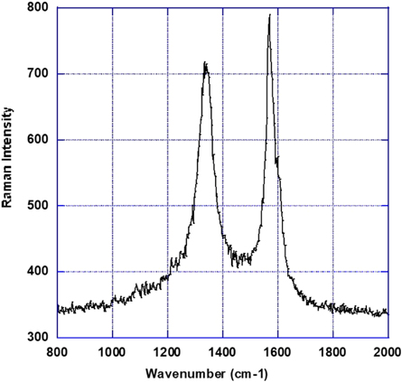
Figure 1. First order Raman spectrum of the graphene powder used in this study recorder with a 532 nm wavelength excitation laser on a glass slide. The spectrum depicting the A1g mode (the D band) and the E2g mode (the G band) at 1340 and 1570 cm−1, respectively.
Download figure:
Standard image High-resolution imageTo prepare the films, first, we dissolved the graphene flakes in dimethylformamide (DMF) (Fisher Scientific, reagent grade). The solution was sonicated for different times, namely, 24, 36, and 48 hours. Then the sonicated solution was centrifuged (Beckman Coulter, AllegraTM X22R) for 30 min at 12000 RPM. The exact concentration of graphene in the extracted sonicated centrifuged solutions was determined to be 0.017 g l−1 by gravimetric evaporation method based on 10 measurements using a balance with 0.1mN sensitivity as described elsewhere [30].
Graphene films were produced using a Langmuir-Blodgett trough (Nima Technology UK, 1222D2). Pure distilled water was used as a substrate for film deposition. Isotherms for the water substrate were run several times to ensure that the water substrate surface was immaculate. Our Langmuir-Blodgett trough is enclosed in a class 100 level clean enclose. 1000 μl of centrifuged graphene flakes in DMF solutions were spread on the subphase surface and left to evaporate the solvent for different times, 30, 120, and 180 min, with an open trough area of 500 cm2. Surface pressure/area isotherms were obtained at a barrier speed of 10 mm min−1. All films in this study were deposited at a constant deposition pressure of 10 mN m−1 within the solid phase on the graphene film, and vertical speed of the substrate of 5 mm min−1. The deposition was achieved by starting the substrates underwater surface and moving the substrate upwards to ensure high transfer rates. Monolayer films were deposited on stainless steel discs for structural characterization using scanning tunneling microscope (STM) (NanoSurf easy Scan, E-Line), on holey amorphous carbon TEM grids for High-resolution transmission electron microscopy (HRTEM) (FEI, Themis Z) characterization, and also on typical laboratory glass slides for UV–IR absorption measurements (Cary® 50 Scans UV Visible Spectrophotometer) as well as electric conductivity. UV-IR absorption measurements were conducted by using a clean glass slide as a reference. The absorption of the reference was subtracted from that of the film on a similar glass slide to show the absorption of the film within the wavelength range tested. The electric conductivity of the films was measured using a modified four-point probe method in which the traditional point probes were replaced by copper strips to avoid film damage. Such modified probes were successfully used before by Li et al. to measure the electrical conductivity of graphene films [31], single-walled carbon nanotube films [32], and C60 HCP monolayer films [33] as well. A counterweight (100 g) was placed during measurements (figure 2) to ensure good contact with the film. It is important to note that with the 100 g counterweight and 80 mm2 of probe/film contact area, the contact pressure between the copper probe and the graphene film is 12.25 MPa. Such contact pressure would not cause plastic deformation into the copper probe and not expected to cause any damage to the graphene film. For each direction, 5 measurements were conducted by pressing the probes against the graphene film in random places to ensure the continuity of the film on a millimeter scale length.
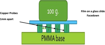
Figure 2. Schematic shows an Illustration of a typical Four-Point probe arrangement.
Download figure:
Standard image High-resolution imageIn brief; film electric resistance was measured by using 4-point probe I-V measurements, and the electric conductivity was determined according to the thin film protocol [34].
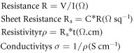
Where C = 4.532 is the geometrical correction factor depends on sample geometry while t is the film thickness in cm. Film thickness was determined using the theoretical thickness of graphene sheet 3.35 Å [7]. Our modified 4-point probe was tested and calibrated using copper and graphite samples of known electric conductivity. The 4-point probe was operated using a Keithley 2401 source meter with the ability to produce and measure currents down to 10 pA, and volts down to 1 μV.
3. Results and discussions
Figure 3 shows a typical graphene unit cell (UC). Graphene unit cell contains 2 carbon atoms making the atomic weight per unit cell equal to 24 g/mole. The unit cell has an area of 5.24 Å2. In a typical Langmuir-Blodgett (LB) isotherm experiment, film area is plotted against the film surface pressure. Such LB isotherm is, in very simple terms, the 2D equivalence of a load-deformation curve that is obtained in a typical axial mechanical testing experiment. Knowing the exact amount of graphene added to the trough enables the calculation of the number of graphene unit cells added and, hence, the film area can be converted into area per unit cell as shown in figure 4. By extrapolating the linear portion of the isotherm to zero surface pressure, the actual area per unit cell in the processed film can be determined [35, 36]. Comparing the actual area per unit cell in the film to that of graphene (5.24 Å2) enables the determination of an average number of graphene layers in the processed film. Our current investigation shows that because the initial graphene powder contained both mono- and multilayer flakes, the solution concentration, sonication time, and evaporation time are crucial for the successful production of a monolayer graphene film. Figure 4 shows an isotherm for a film that lacked the optimum initial concentration and sonication time. As shown in figure 4, the average area per unit cell at zero applied surface pressure determined from the linear fit to the LB isotherm is 0.3788 (Å2) indicating that the film has an average of (5.24/0.3788) about 14 layers.

Figure 3. Schematic of Graphene structure and unit cell dimensions.
Download figure:
Standard image High-resolution image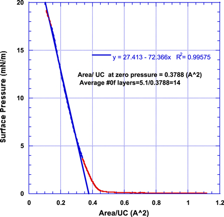
Figure 4. Typical Langmuir-Blodgett isotherms for graphene films sonicated for 48 hours in DMF (0.178 g l−1) and allowed to evaporate for 120 min showing the average number of graphene layers as 14.
Download figure:
Standard image High-resolution imageFigure 5 shows the average film number of layers as a function of solvent evaporation time for initial concentration (0.17 mg ml−1). From this figure, we can realize in general, the evaporation time of the solvent has an insignificant effect on reducing the average number of graphene layers at this concentration. In other words, at high concentration of GNFs, the produced graphene film has predominant multi-layers graphene with an average number of layers ranging 9–22 even though a long sonication time has been used. The increase in the average number of layers for 24 and 36-hour sonication could be attributed to the tendency of GNFs to re-aggregate and agglomerate around the undissolved particles due to the high surface tension of small flakes and the large particles size of undissolved GNFs at this concentration [37, 38].

Figure 5. Minimum average film number of layers as a function of evaporation time of solvent for 0.17(g l−1) GNFs concentration.
Download figure:
Standard image High-resolution imageFigure 6 shows a 20 × 20 nm 3D STM image of the structure of a multi-layer graphene flakes film. It is important to note the clear terrace structure observed which can be attributed to lack of sonication and high concentration of the processing solution.
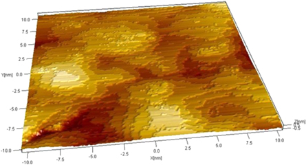
Figure 6. 20 × 20 nm STM image of a multi-layer graphene film showing a terrace-like structure.
Download figure:
Standard image High-resolution imageThe GNFs concentration was then diluted to be (0.017 g l−1), and we observed the average number of layers at different evaporation time, as seen in figure 7. The data shows that at such level of dilution, the sonication and evaporation time effect on the number of layers becomes significant. However, the minimum average number of graphene layers obtained at these conditions was predominantly ∼2–3 layers.

Figure 7. Minimum average film number of layers as a function of evaporation time of solvent for 0.017(g l−1) GNFs concentration.
Download figure:
Standard image High-resolution imageMonolayer graphene films were only produced as we decreased the graphene/DMF solution concentration to 0.0089 mg ml−1. Our investigation shows that truly monolayer graphene films can be processed successfully using a concentration of 0.0089 mg ml−1 sonicated for 48 hours and then allowed the DMF solvent to evaporate on the open Langmuir trough for 2 h.
Figure 8 shows a LB isotherm for a true monolayer graphene film. It is important to note that the actual area per unit cell in the film is determined to be 5.1 Å2, that is 97% of the theoretical value of the graphene unit cell at 5.24 Å2. This is expected, however, considering the flake edges with broken hexagons leading to a smaller (on average) area per unit cell in a well-pressed continuous film.
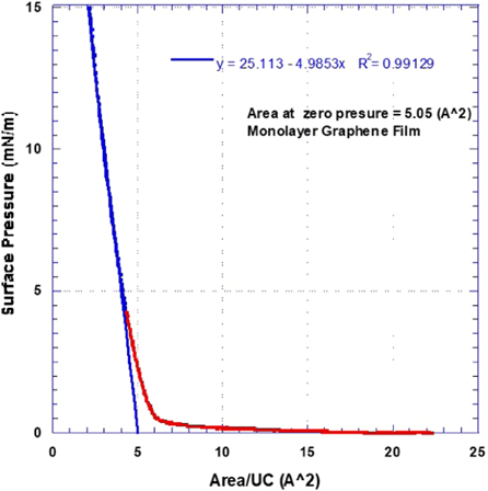
Figure 8. Langmuir-Blodgett isotherm for a mono-layer graphene film sonicated for 48 hours in DMF (0.0089 g l−1) then allowed to evaporate for 180 min.
Download figure:
Standard image High-resolution imageVerification of film structure using HRTEM, STM, and AFM microscopy confirmed the monolayer nature of the film, as shown in figures 9, 10(a), (b), 11, and 12. high-resolution transmission electron microscopy (HRTEM) image of a monolayer film deposited on TEM grid confirms the monolayer nature of the produced film, as shown in figure 9. Figures 10(a) and (b) both show 3D STM images of the film confirming the continuity (over nanometer length scale), and the monolayer nature of the film (note the picometer scale in the film thickness direction). Figure 11, a 200 × 200 nm high resolution picture from STM scan operated in the current mode provides an excellent experimental result for the monolayer nature of the film as well as a clear view of the individual graphene flakes. Note that the average flake size is ranging between 10 and 30 nm. In addition, the AFM scan (figure 12) confirms the continuity and homogeneity of the film on the micrometer length scale. Finally, figure 13 shows optical pictures of the glass slide substrate before and after being coated with the monolayer graphene film. The set of pictures clearly demonstrate the transparency of the film. More importantly, the coated glass slide exhibits a clear hydrophilic surface as proved by the behavior of water droplets deposited on the glass surface. The pictures also provide an undisputed proof for the homogeneity and continuity of the film on a large scale.

Figure 9. The HRTEM image of the structure of a monolayer graphene film deposited on TEM grid holder.
Download figure:
Standard image High-resolution image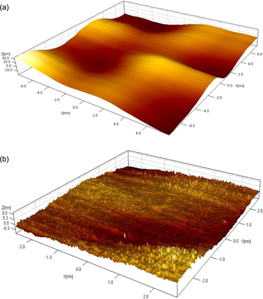
Figure 10. (a) A 16 × 16 nm STM image of the monolayer graphene film. (b) A 5 × 5 close-up on the part of the image in 10.a. Note the pico-meter range of the z-axis.
Download figure:
Standard image High-resolution image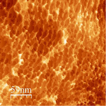
Figure 11. A 200 × 200 nm high-resolution scan using STM (in current mode) showing the structure of graphene mono-layer film with the individual graphene flakes. Note the average graphene flake size that is ranging between 10 and 30 nm.
Download figure:
Standard image High-resolution image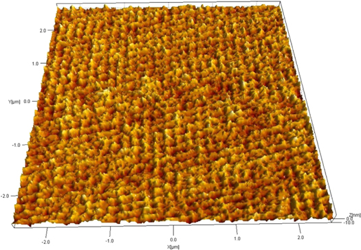
Figure 12. A 6 × 6 micron AFM image providing evidence of the film homogeneity and continuity at micron scale length.
Download figure:
Standard image High-resolution image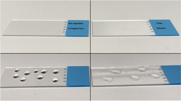
Figure 13. Optical pictures of uncoated and graphene coated glass slides before and after depositing micro-water droplets on them. Note the hydrophobic nature of the coated glass slide and the homogeneity of the film on the whole glass surface.
Download figure:
Standard image High-resolution imageAs we discussed in earlier publication [29, 32, 33] the Langmuir-Blodgett isotherm can be converted into a film stress-strain curve by dividing the surface pressure (N m−1) by the film thickness of a monolayer graphene ( 3.35 Å) [39], and by transforming the film deformation into film linear strain since the film width is constant in all experiments (same as trough width that is equal to 0.2 m). Figure 14 shows the compressive stress-strain curve for the monolayer graphene film (obtained from the isotherm shown in figure 8).
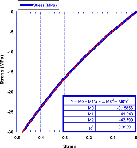
Figure 14. Compressive stress-strain curve of the graphene mono-layer film. Note the non-linear behavior.
Download figure:
Standard image High-resolution imageIt is essential to note the non-linear behavior of the graphene film under compressive stresses and its high ability to compress (@47.5%) while still intact. The film behavior fits exactly (R2 = 0.99991) a second-degree parabola equation of the form:

Hence, the film elastic modulus (E = dσ/dε) exhibits a linear dependence on the applied compressive strain of the form:

As shown in figure 15, the monolayer graphene film processed in this study exhibits an apparent non-linear compressive stress-strain behavior with a linear stiffening behavior as the film is compressed. Such behavior is similar to graphene behavior under tensile stress as reported by Lee et al [13]. who reported a strain-softening behavior under tensile stresses and predicted strain stiffening behavior under compressive stress. Our current experimental measurements are also in agreement with the nonlinear elastic response of graphene sheets previously suggested by numerical simulations [14, 40]. It is important to emphasize that such nonlinear behavior was observed neither in hexagonal close-packed C60 monolayer films [29] nor in aligned single-walled carbon nanotube (A-SWCNT) films [32]. Comparing the monolayer graphene film stiffness (40 to 80 MPa) to that of C60 and A-SWCNT films, the graphene monolayer film is much stiffer since the stiffness of C60 films was reported to be 32 ± 1 MPa, and that of A-SWCNT was reported to be 10 ± 0.5 MPa.

Figure 15. Elastic modulus of the graphene mono-layer film as a function of film strain. Note the clear linear strain stiffening behavior.
Download figure:
Standard image High-resolution imageFigure 16 depicts the absorbance (%) within the range ±0.05% (y-axis has been selected in that range to show the negligible experimental measurements noise) as a function of the light wavelength (nm) of our monolayer graphene films. The measured absorbance of the film after subtracting that of a reference identical clean glass slide is found to be 0.05% which is practically zero absorbance. Hence, the produced films exhibit a constant value of full transparency within the measured range (400 nm—1100 nm). Our current results are different from the results of Nair et al [41] who measured the light transmittance of CVD monolayer graphene deposited on a steel substrate with 50 μm holes and reported a 2.3% light absorbance for the monolayer graphene film in the wavelength range between 400 nm and 700 nm. The difference between our results and the results reported by Nair et al can be attributed and explained by the difference between their test and ours. In our measurements, the film is made of graphene nano-flakes with many flake boundaries deposited on an insulating glass slide. Nair's measurements, however, were on pristine graphene film suspended in air (over the 50 μm hole) while supported by a conducting steel substrate. The graphene edge effect, the suppression of out-of-plane vibration modes in substrate supported graphene, and substrate interaction and their impact on electro-optical and even mechanical properties of carbon nano-structures has been observed and discussed widely before [28, 42]. A systematic study to investigate the effect of substrate on electro-optical properties of monolayer graphene would definitely sheds more light on such important point.

Figure 16. UV-visible spectrophotometer for the graphene film.
Download figure:
Standard image High-resolution imageFigure 17 depicts the measured electric conductivity of our films in both deposition (longitudinal) and transverse directions. No significant difference is observed indicating a non-preferred orientation of the GNFs within the film. The measured electric conductivity of the film is1.08 * 104 S cm−1. While this value is about two orders of magnitude lower than the highest intrinsic conductivity value (1.1 * 106 S cm−1) measured for Langmuir-Blodgett graphene films at liquid helium temperature [43] and the theoretical limit of monolayer pristine sheets [7, 44], it is almost the same as the conductivity values measured at room temperature and reported for continuous monolayer graphene films produced by CVD as well as reduction methods [45–48]. Our current results show that flake edge effects on the electrical conductivity [42]. Can be minimized once film processing parameters are well optimized and films are deposited at deposition pressures ensuring good substrate coverage.

Figure 17. Electrical Conductivity (S/cm) of the graphene film in the longitudinal and transverse direction. Note that error bars of 5 random measurement of the film conductivity provides evidence of the film homogeneity and continuity at the millimeter length scale.
Download figure:
Standard image High-resolution image
To this end, and giving the fact that the continuity and uniformity of the produced mono-layer films is shown on different length scales; the Angstrom scale (HRTEM image), the nano-scale (STM images), millimeter-scale, (electrical conductivity measurements), and the centimeter-scale (mechanical testing within LB trough), it is clear that LB technique is very valuable tool to produce continuous mono-layer graphene films with many advantages over other production methods used currently in the field.
4. Conclusions
We have managed to process truly monolayer graphene films using graphene flakes and Langmuir-Blodgett technique. Mono-layer films will only be produced under specific processing conditions or solution concentration, sonication time, and solvent evaporation time. Such conditions are expected to be solvent dependent as well. The films exhibit a nonlinear compressive stress-strain behavior with a stiffening behavior. The film stiffness is higher than similar monolayer films made of C60 fullerenes and aligned single-walled carbon nanotubes. Also, the graphene film obtained an excellent electrical conductivity with full transparent as well.
Acknowledgments
Professor Amer greatly acknowledges the generous Fulbright fellowship allowing the use of King Abdulla University of Science and Technology (KAUST) electron microscopy facilities. Mr Mohammed greatly appreciates the fellowship received from the Higher Education Council of Iraq to pursue his Doctoral Degree at Wright State University.