

Abstract
Spin transport properties of zigzag silicon carbide nanoribbon (ZSiCNR) which includes four edge contacts are studied by the first principle method. All possible configurations are: (a) each edge carbon (C) and silicon (Si) atoms passivated with one hydrogen (H) atom (1H-1H), (b) each edge C atoms and Si atoms passivated with two H atoms (2H-2H), (c) each edge Si atoms bonded with one H atom and each edge C atoms bonded with two H atoms (1H-2H), and (d) edge C atoms saturated with one H atom and edge Si atoms saturated with two H atoms (2H-1H). Based on our results, three of these structures show the perfect spin filtering effect (100%) in the applied bias region (0.0 V to 0.5 V), which can be used to design spin polarizer devices. Besides, the current-limited effect is observed in the 1H-1H configuration under the bias voltage. Moreover, the negative differential resistance phenomenon is specified in the spin-polarized current for 2H-2H structure. Our findings show that suggested structures exhibit some interesting spin-dependent transport properties.
Export citation and abstract BibTeX RIS
1. Introduction
Spintronic properties of graphene as a two-dimensional (2D) material have attracted considerable attention in recent years [1–3]. However, the zero-energy gap of the graphene has limited its applications in various industries [4–6]. For this reason, the 2D graphene-like materials such as IV group semiconductors (SiC, SiGe, GeC, SnC, SnSi, GeSn), with sufficient bandgap, could enrich the family of 2D electronic materials [7–10]. Among these materials, 2D silicon carbide (2D SiC) is widely studied due to its exciting spin-dependent properties [11, 12]. The 2D SiC is similar to graphene or hexagonal boron nitride (h-BN) sheets, but the bond length of Si-C (∼1.79 Å) is larger than C-C (1.42 Å) [13], and B-N (1.44 Å) bond length [14]. The cutting of SiC sheets construct the SiC nanoribbons (SiCNRs), just like in producing graphene nanoribbons. Similar to graphene, the edge carbon and silicon atoms of SiCNR are passivated by a hydrogen atom, which is called as the H-passivated SiCNR. The magnetic and electronic properties of the H-passivated SiCNRs are investigated extensively by using the first-principle method. Zheng et al found that the H-passivated zigzag SiCNR (1H-ZSiCNR-1H) is the ferrimagnetic semiconductor with the direct bandgap (2.55 eV) [15] while armchair SiCNR (1H-ASiCNR-1H) is the nonmagnetic semiconductor [16]. The magnetization of 1H-ZSiCNR-1H can be manipulated by applying an electrical field [17], carrier doping (hole and electron) [18, 19], and creating the vacancy [20, 21]. Recently, Lou studied the effect of edge reconstruction and boron/nitrogen doping on the H-passivated ZSiCNR [22, 23]. He observed the magnetic and half-metallic behaviours in ZSiCNR. Also, Guan et al demonstrated that the fully hydrogenated ZSiCNRs and ASiCNRs, with different ribbon widths, are all nonmagnetic semiconductors [24]. An et al have investigated the spin transport of 1H-ZSiCNRs-1H in the metallic ferromagnetic (FM) ground state and the half-metallic antiferromagnetic (AFM) ground state under the bias voltages [7]. They found that 1H-ZSiCNR-1H in FM ground state shows the spin filtering effect while in AFM ground state. The 1H-ZSiCNR-1H shows the abnormal spin-dependent current behaviour. Furthermore, Lou considered four possible edge contacts of ZSiCNR and he studied the effect of edge hydrogenation on the stability, electronic and spin transport properties of them [11]. His results displayed that the electronic and magnetic properties of H-passivated ZSiCNR depend on the ribbon width. In addition, he only analysed the transmission spectra of 2H-ZSiCNR-2H and 2H-ZSiCNR-1H in different widths of nanoribbons.
On the other hand, the experimental conditions, such as finite temperature and the hydrogen content of the environment, could influence the magnetic and electronic properties of ZSiCNR. In addition, many theoretical studies, which presented in the literature of ZSiCNR, focused on single hydrogen passivated of each edge. Therefore, further studies are needed to fully understand the effect of the edge hydrogenation on the spin-dependent current properties of H-passivated ZSiCNRs. These features can be used to find the appropriate potential applications in the spintronic devices. Therefore, we investigate the spin-dependent transport properties of four H-passivated ZSiCNRs. The infinite six zigzag chains of SiCNR are constructed and divided into three parts: the left electrode (L), the scattering central region (C), and the right electrode (R). Each edge atom of ZSiCNR is passivated by one hydrogen atom, as shown in figure 1. The Si (C) atoms are in the upper (lower) edge.

Figure 1. Cross-section view of zigzag SiCNR with six chains in width under the bias voltage. Each edge C (Si) atoms are passivated with one hydrogen. The structure is divided into three sections: the left electrode, the scattering region, and the right electrode which marked by L, C, and R, respectively.
Download figure:
Standard image High-resolution imageThe spin transport properties are studied by using non-equilibrium Green's functions (NEGF) [25] and Landauer–Buttiker approach [26] in the framework of density functional theory (DFT) [27, 28]. In the present paper, spin-filtering efficiency (SFE) can be reached as high as 100% in such configurations. Furthermore, the negative differential resistance (NDR) phenomenon and the current-limited effect are observed. The mechanisms of the spin filter and the spin current are explained for all configurations. The paper is organized as follows; in the next section, the method and computational details will be briefly described. In section 3, our results are discussed, and finally, the paper has ended with brief conclusions.
2. Computational method
The two side edges of ZSiCNR are terminated by C or Si atoms and are called the C-edge and the Si-edge, respectively. The edge hydrogenation is accomplished when the H2 gas is applied to pristine ZSiCNR. One hydrogen atom (sp2 hybridization) or two hydrogen atoms (sp3 hybridization) can saturate the C-edge and Si-edge. Accordingly, the four possible hydrogen terminations can exist that are shown in figure 2.
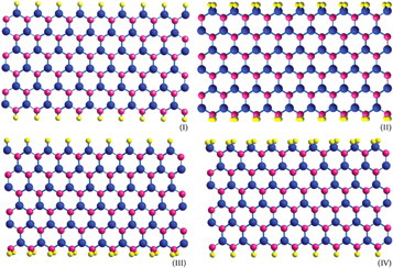
Figure 2. The edge C or Si atoms are bonded with different hybridizations. The blue spheres denote Si atoms; the red (yellow) spheres denote C (H) atoms. The geometric structures for the (I) 1H-1H, (II) 2H-2H, (III) 1H-2H (IV) 2H-1H.
Download figure:
Standard image High-resolution imageThese configurations, as mentioned, are including (a) 1H-ZSiCNR-1H (1H-1H), (b) 2H-ZSiCNR-2H (2H-2H), (c) 1H-ZSiCNR-2H (1H-2H), and (d) 2H-ZSiCNR-1H (2H-1H). Each electrode in these devices is described by a supercell with two repeated unit-cells along the transport direction, and the scattering region is the ZSiCNR with five unit-cell lengths.
The geometry optimizations and the calculations of electronic and spin transport properties are performed in the framework of DFT and NEGF as implemented in the TranSIESTA [29] module within the SIESTA package [28]. The exchange-correlation functional of the generalized gradient approximation (GGA) is framed by the Perdew–Burke–Ernzerhof approximation [30]. Also, Troullier-Martin type norm-conserving pseudopotentials are employed in our calculations [31].
The energy cut-off is chosen 300 Ry in numerical integrations for the real-space grid, and the mixing factor is considered 0.1 in the self-consistent calculations. The geometrical structures are optimized until all forces on each atom are smaller than 0.04 eV Å−1. The wave function of atoms is extended via a double-zeta polarized (DZP) basis set, and the Monkhorst-Pack k-point mesh [32] is adopted 1 × 1 × 12 in the x, y, and z directions, respectively.
For the investigation of the spin-dependent transport properties, the transmission coefficient and the spin-dependent current are calculated via the Landauer-Buttiker formalism as follows:

Where the σ is equal to ↑ (spin-up) and ↓ (spin-down). The  and
and  are defined as the Fermi–Dirac distribution function of the left (right) electrodes and the bias voltage, respectively. The difference between the chemical potentials of the left and right electrode is
  The integral region in equation (1) defines as the bias window (BW) from −eVb/2 to +eVb/2. The Tσ as the spin-dependent transmission coefficient is given by:

Where  is the contact broadening function of the right (left) electrode and
  is retarded (advanced) Green's function of the scattering region.
3. Results and discussions
The stability and formation energy of four structures in different widths are investigated by Lou [11]. All structures have negative formation energy except 1H-1H formation, so they are stable in experimental situations. Also, his results have displayed that in the zero temperature (T = 0K), the 2H-2H nanoribbons are the most stable edge hydrogenated structure instead of the 1H-1H configuration. Furthermore, comparing of formation energy in 2H-1H and 1H-2H has specified that two hydrogen atoms prefer to occupy the Si-edge and make sp3 hybridization.
To distinguish between four structures, the interchange charge density and the magnetic moment of double and single terminations are analysed. The magnetic moment of each edge atom and its nearest-neighbouring atom are tabulated in table 1. The HC and HSi indicate hydrogen passivated of edge C atom and edge Si atom, respectively. In addition, the spin densities of four structures are shown in figure 3. In the 1H-1H configuration, the magnetic moments are localized on each edge C atoms and edge Si atoms while inter edge C atoms at the Si-edge (inter Si atoms at C-edge) carry very small magnetic moments.
Table 1. The magnetic moments at edge C (Cedge) and Si (Siedge) atom, at the nearest-neighbouring atom of the edge atom (SiC-edge and CSi-edge) and the saturated hydrogen atoms (HSi and HC). (The unit of magnetic moment is μB).
| System | Siedge | Cedge | SiC-edge | CSi-edge | HSi | HC |
|---|---|---|---|---|---|---|
| 1H-1H | −0.266 | 0.235 | −0.021 | 0.047 | 0.008 | −0.006 |
| 1H-2H | 0.33 | −0.032 | 0.548 | −0.055 | −0.011 | 0.026 |
| 2H-1H | −0.002 | 0.303 | −0.028 | 0.41 | 0.065 | −0.007 |
| 2H-2H | −0.001 | −0.027 | 0.44 | 0.32 | 0.056 | 0.023 |
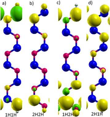
Figure 3. The spatial distribution of the spin differences for the ZSiCNR (a) 1H-1H, (b) 2H-2H (c) 1H-2H, and (d) 2H-1H configurations, the yellow and green surfaces represent the density of spin-up and spin-down states, respectively. The blue spheres denote Si atoms; the red (grey) spheres denote C (H) atoms.
Download figure:
Standard image High-resolution imageContrary to the configuration of 1H-1H, in the 2H-2H case, the magnetic moments of inter edge C atoms at the Si-edge and inter edge Si atoms at the C-edge are more than the magnetic moments on each edge C atoms and edge Si atoms. In the next step, the magnetic moments of 1H-2H are compared with 1H-1H configuration. It is clear; hydrogenation of edge C atom with two H atoms leads to the charge of C atom transfers to the nearest-neighbouring Si atom of the edge C atom (SiC-edge). In the 2H-1H configuration, when the edge Si atom passivated with two H atoms, the charge of Si atoms moves to CSi-edge atom (the nearest-neighbouring C atom of the edge Si atom) and the nearest neighbouring of edge Si atom has the highest value of magnet moment and charge density. These points are determined in figure 3, and the obtained results are in good agreement with the previous study [11].
After analysing the structural properties of four configurations and finding the difference between them, their spin-dependent transport properties are discussed. At first, the current as a function of the applied bias voltage from 0.0 to 0.5 eV (I–V characteristics) are shown in figure 4. Since our structures are symmetrical in both the electrodes, the results will be identical for the negative and positive biases.
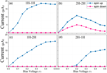
Figure 4. The spin-dependent I–V curves for (a)1H-1H, (b)2H-2H, (c)1H-2H, and (d)2H-1H structures.
Download figure:
Standard image High-resolution imageIn figure 4(a), the spin filtering effect is observed in the 1H-1H structure. The spin-up current raises as to the bias increases from 0.0 V to 0.35 V and reaches a maximum value of 18.55 μA. Beyond 0.35 V, the spin-up current is approximately constant under increasing the bias voltages, and the current-limited effect occurs for the voltage range of [0.35–0.5] V. In addition, among the four configurations listed, the 1H-1H structure has the highest values of spin-current.
The I–V characteristic of 2H-2H configuration in figure 4(b), show the negative differential resistance (NDR) properties. The spin-up and spin-down currents increase by increasing the bias voltage from 0.0 V to 0.2 V. The maximum values of spin-up and spin-down currents are 10.84 μA and 4.99 μA, respectively.
Beyond the 0.2 V by increasing the voltage, the spin currents decrease and reach the minimum values of 4.5 μA and 1.01 μA at 0.5 V for the spin-up and spin-down states, respectively. The peak-to-valley ratio (PVR) for the spin-up current is 2.4. The spin-down current magnitude is comparatively lower, so its PVR is 4.94, about five times the PVR of the spin-up current. The obtained PVR, in this case, is comparable with the other studies [33, 34]. Accordingly, 2H-2H configuration can be used as FET devices with the NDR properties under optimized source, drain, and gate potential.
The I-V curves in the 1H-2H configuration are illustrated in figure 4(c). These curves show significant spin splitting with perfect spin-filtering behaviour (100%). The spin-up current increases by increasing the bias voltage up to 0.4 V, and then; the gradient of the I-V curve is reduced. The current of spin-up states reaches the maximum value of about 15.87 μA.
Figure 4(d) displays spin filtering behaviour in the 2H-1H case. Before 0.1 V, the spin-up current is almost zero, and then it increases when the bias rises from 0.15 V to 0.5 V. The current maximum value of the 1H-1H structure is twice (1.7) as high as this case.
Next, the spin filtering efficiency (SFE) of four configurations with SFE = (Iup − Idown/Iup + Idown) is calculated, where Iup and Idown are the spin-up current and spin-down current, respectively. Figure 5 shows the SFE as a function of applied bias voltage. The SFE of 2H-2H configuration is about 37% in the range of 0.05 V to 0.25 V and after that, it grows and reaches 61% at 0.5 V bias voltage.
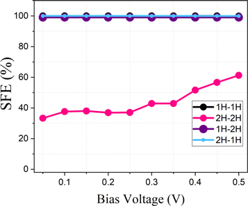
Figure 5. The spin filter efficiency (SFE) of 1H-1H, 2H-2H, 1H-2H, and 2H-1H configurations.
Download figure:
Standard image High-resolution imageFor 1H-1H and 2H-1H and 1H-2H structures, the SFE is higher than 99% in the bias range from 0.05 to 0.5 V. It means that the currents of spin-up sates flow from left electrode to the right electrode while the spin-down currents are forbidden. Therefore, all the mentioned structures can act as a spin filter device at low temperatures. These results are comparable to other theoretical studies [35, 36].
Distinctive spin transport behaviours, namely the spin filtering effect, NDR phenomenon, and current-limited effect could be discovered through the band structure of electrodes and the transmission spectrum of the scattering region. For this reason, the spin-polarized transmission coefficient of the central region versus energy is plotted at a specific bias voltage, and it compared to the band structures of the left and the right electrodes. As shown in figure 6, the opposite shift of chemical potential in the left electrode and the right electrode form the bias window (BW).
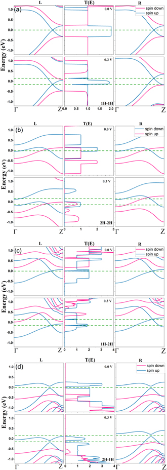
Figure 6. Band structure of the left electrode, transmission spectra of the central region and the band structure of right electrode under 0.0 V and 0.3 V bias for (a) 1H-1H, (b) 2H-2H, (c) 1H-2H (d) 2H-1H. The blue (red) lines denote spin-up (down) state. The green dashed line refers to the bias window. The Fermi level is set to zero.
Download figure:
Standard image High-resolution imagePrevious studies have shown that when only the similar spin state bands of the left and right electrodes overlap within the BW, the transmission channel will be open and the spin-dependent current obtains [37]. Thus, the tunnelling of the same spin state is achievable for the structures. In other words, if the opposite spin state bands are present in BW, the transmission channels are closed and the spin current is forbidden.
We considered the condition of applied bias in 0.0 V and 0.3 V in figure 6. When the voltage bias applies, the location and the shape of the transmission peak change. At 0.3 V, the BW is equal to [−0.15–0.15] V (BW is obtained by [−eVb/2, +eVb/2] in equation (1)).
As can be seen in figure 6(a), the band structures of the left and the right electrodes are the same in zero bias because the symmetry of both electrodes, similar sub-bands spin state are present. Around the Fermi level, the present of spin-up bands in two electrodes causes the high and broad spin-up transmission coefficients. Since the spin-down bands are located lower and higher than the Fermi level, they have not crossed this level. Therefore, the transmission channel for the spin-down states is closed. In other words, the transmission spectrum of the spin-down electrons demonstrates a gap (0.54 eV) around the Fermi level because the spin-down bands of two electrodes have a gap (0.54 eV) in this area.
When a bias is applied to both electrodes, the band structures of the left and the right electrodes shift downward and upward, respectively. The moving down and up of the band structures lead to the change in the overlapping of spin state bands within the BW.
As can be seen in figure 6(a), by increasing the bias voltage, the current integral area increases. The transmission coefficients grow up to 0.35 V. Furthermore, the spin-up bands of the left and the right electrodes show a significant overlap within the BW. Therefore, the transmission of the spin-up electrons is allowable through the nanoribbon as well as the spin-up current. The spin-down bands of the left and the right electrodes did not overlap within the BW. Therefore, the spin-down current is zero, which is a necessary characteristic of a perfect spin filtering effect. Our results have a good agreement with the previous work [7]. In addition, the current-limited effect occurs when the bias voltage increases from [0.35–0.5] V. The degree overlaps between the bands of the left and right electrodes decrease and the transmission gap near the Fermi level increases. Therefore, inside the BW, the areas of the transmission are almost constant, and subsequently, the current-limited effect occurs.
For the 2H-2H configuration, the transmission spectrum and the band structures of the left/right electrodes are shown in figure 6(b). At a bias of 0.0 V, the transmission spectrum exists for both spin orientations because both spin state bands are present in two electrodes near the Fermi level. Therefore, there is the possibility of overlapping both spin states, and the transmission channel is opened for the up and down spins. As the bias voltage increases, the current integral area increases up to 0.2 V bias. Beyond 0.2 V bias by increasing the bias voltage the transmission coefficient decreases, and this device shows the spin-polarized NDR characteristics for both spin orientations.
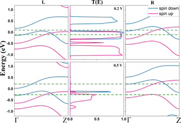
The Originated of NDR is explained by the spin-polarized transmission spectrum and the corresponding left and the right band structures of electrodes under bias voltages [38, 39]. In order to investigate the NDR phenomenon, we consider the condition of applied bias in 0.2 V and 0.5 V (it can be seen in figure 7). The I-V curve shows that in 2H-2H structure (figure 4(b)); the transmission coefficient in 0.2 V is the maximum value among mentioned bias voltages (such as 0.5 V). Before 0.2 V, by increasing the bias voltage, the spin state bands have maximum overlap within the BW. Therefore, the transmission coefficient and the spin current is the maximum value. Then, by increasing the bias voltage, the overlapping of spin bands from two electrodes decreased. Consequently, it leads to the decreasing of the transmission coefficient and the NDR phenomenon occurs (as can be seen in figure 7 (0.5 V)). The spin-down transmission spectrum has a lower coefficient than spin-up states under all bias voltages, so the current of spin-down states is always less than the spin-up current.
Figure 7. Band structure of the left electrode, transmission spectra of the central region and the band structure of the right electrode under 0.2 and 0.5 V bias for 2H-2H. The blue (red) lines denote spin-up (down) state. The green dashed line refers to BW.
Download figure:
Standard image High-resolution image
Figure 6(c) shows that only the spin-up bands are present near the Fermi level, while the bandgap of spin-down states is 2.46 eV. When the bias voltage is applied to the system, (in figure 6(c) under 0.3 V), the spin-down bands are still not present in the BW, and the transport channels of this spin orientation will remain closed. As a result, the spin filtering effect has happened for the 1H-2H configuration. The last structure, 2H-1H, has the same behaviour as 1H-1H and 1H-2H. However, in figure 4(d), the I-V characteristic displays that the spin-up current increases significantly after the bias voltage 0.1 V. To understand this, the band structures of two electrodes in figure 6(d) should be considered. As shown, spin-up bands are located near the Fermi level with a distance of approximately 0.1 eV, and they do not cross this level. Therefore, after 0.1 V, the current reaches a μA order.
Another point is that the SEF reported in figure 5 is 100%, even under a voltage lower than 0.1 V since, in the range of [0.0–0.1] V; the spin-up current (the order of magnitude of 10–11 μA) is much larger than the spin-down current (the order of magnitude 10–16 μA). Therefore, the SEF can be enlarged as high as 100% under any bias voltage. As a significant result, the transmission gap of spin-down states around the Fermi energy is extended by increasing the bias voltage, and then spin-down electrons cannot propagate through the nanoribbon (figure 6(d)). On the other hand, the spin filtering can be controlled via manipulating the bias voltage.
From a blended analysis of the spin-dependent transmission spectrum and the band structure, we conclude that the edge hydrogenation of SiCNR changes the bands around the Fermi level and it will cause the nanostructure devices generated with a good spin filter and NDR properties.
4. Conclusions
In summary, the spin-dependent transport properties of ZSiCNRs in the presence of edge hydrogenation are investigated by using non-equilibrium Green's functions (NEGF) in the framework of density functional theory (DFT). Four possible H-passivated edge configurations are considered. The spin density and the magnetic moment of double and single terminations are analysed to differentiate between four structures. The results of I-V characteristics show the perfect spin filtering effect (100%) in 1H-1H, 1H-2H, 2H-1H cases. Therefore, these structures have potential applications in spintronic devices. Moreover, the current-limited effect and negative differential resistance (NDR) phenomenon are observed in the 1H-1H and 2H-2H cases, respectively. Our results have shown that the transport coefficients, as well as spin currents, are non-zero when the same spin bands overlap within the specific BW region. These results can imply the potential applications in spintronic industry, which included such as logic, amplification, and memory.
Acknowledgments
This work was supported by Iran University of Science and Technology (IUST) Grant No. 160/482.