

Abstract
This study focuses on aiming higher stabilized sunlight to electricity conversion efficiency for Cadmium Telluride (CdTe) absorber based solar cell. Common CdTe solar cell with Au back or Zinc Telluride (ZnTe) back surface field (BSF) with Cu back metal has voltages < 1V. The reason behind this low voltage has been investigated in details. In this report, simulation yielding of (M = Cu, Ni, Au, Ir, Pd, and Pt) thin-film solar cell (TFSC) has been presented. The solar cell has been modelled and analyzed using Analysis of Microelectronic and Photonic Structures – 1 Dimensional (AMPS-1D) device simulator for various back metals with work function, Φm ≥ 5 eV. The thickness was varied from 100–1800 nm, and from 15–100 nm for the active p-CdTe absorber, and n-Cadmium Sulphide (CdS) window layers, respectively, to optimize the device depth. Meanwhile, the donor and acceptor concentration was varied to outline their effects on photovoltaic (PV) parameters. The utmost efficiency (η) of ∼30% along with open circuit voltage of 1.194 V, short circuit current density of 28.6 mA cm−2, and fill factor (FF) of 89.3% has been achieved ideally with Platinum (Pt) back contact at (111) plane under standard test conditions (STC) of and 1 Sun illumination (1000 W m−2) at air mass (AM) 1.5. Lastly, the cell operating temperature was varied from to to verify the thermal stability of the proposed structure. Present work provides a guideline to select back metal in CdTe solar cell. Our proposed solar cell offers the prospect of being a highly efficient cost effective second generation (2G) TFSC.


1. Introduction
Solar cell devices exploit the photovoltaic (PV) effect, whenever they are exposed to solar radiation. When sufficiently energized photons from sunlight strike the junction of a solar cell and if the photon energy exceeds the band gap energy of the active material of the cell, photons are absorbed by the cell active (absorber) material. Then positive and negative charge carriers namely holes and electrons are generated. In the cell junction, the built-in-potential barrier works on these electrons to introduce a potential difference called the photovoltage used to drive the photogenerated direct current through the external electric circuit.
Major second generation (2G) thin-film PV solar cells include Hydrogenated amorphous-Silicon (a-Si:H), Cadmium Telluride (CdTe), Copper Indium-Selenide (CIS), Copper Indium Gallium-di-Selenide (CIGS) based solar cells [1]. CdTe thin-film solar cell (TFSC) is a leading and prominent candidate of the 2G TFSCs because of its optimum band gap energy of 1.45 eV and high absorption coefficients of [2].

Forming from Cadmium (Cd) and Tellurium (Te), CdTe becomes a stable crystalline compound. Cadmium sulphide (CdS) is an II–VI semiconductor consisting of Cd from group II and Sulphur (S) from group VI of the periodic table of elements. Typical CdTe solar cell comprises of CdTe material as p-type absorber layer, CdS window layer as n-type heterogeneous partner, a metallic layer as the back contact, transparent conductive oxide (TCO) layer as the front contact, soda lime glass (SLG) as the substrate, and an anti-reflection coating (ARC) layer to minimize the amount of photons to be reflected back from the incident surface. It is found [3] that CdS, as n-type material, is best suited to make the hetero-junction between CdTe and CdS for having solar cells with high efficiency and low cost due to their chemical and optoelectronic properties matched between them.
Two Cadmium molecules—CdTe and CdS result ease in manufacturing CdTe TFSC comparing to the multi-step process of joining two differently doped Silicon (Si) materials in traditional Si wafer based technology. Cadmium is abundant and produced as a by-product of other important industrial metals such as Zinc. It has not had the wider price swings that happened with silicon prices. For CdTe modules, the seasonal performance changes are less pronounced compared to amorphous silicon (a-Si) technology [4]. Using Magnesium Chloride (MgCl2) instead of Cadmium Chloride (CdCl2) in fabricating CdTe solar cell, environmental risk and cost of fabrication of CdTe solar cell can be minimized significantly [5] in existing CdTe solar cell production.
The compound semiconductor material CdTe is currently being used to produce TFSCs with least cost in multi kilowatt systems [3]. PV module production and percentage of thin-film market share for CdTe thin-film solar cell technology is significantly higher than other two thin-film technologies of amorphous silicon and CIGS thin-film [6]. The Topaz Solar Farm employed 9 million CdTe modules for 550 Mega Watt power in California which was the world's largest PV power station in 2014 [7]. Nowadays, CdTe modules are produced on the Giga Watt-peak per year level and currently are the cost leader in the photovoltaics industry [8]. Among any other thin-films, CdTe PV modules represent 80% of the total production [9].
In Analysis of Microelectronic and Photonic Structures – 1 Dimensional (AMPS-1D) [10] simulator, efficiency of 18.3% [3], 20.342% [1], 24.755% [2] was achieved with 1μm thick CdTe absorber layer. Currently First Solar Inc. is the number one manufacturer of solar PV modules in the world and also the leading manufacturer of the CdTe thin-film solar PV modules [7]. The First Solar Inc. proclaimed that their CdTe cell has obtained a record cell efficiency of 22.1% in February 2016 [7, 11] that outdid polycrystalline Silicon record cell efficiency of 21.3%. In the empirical roadmap for mid-term of 2019–2020 (probably) the target of getting 24% efficiency has been announced [12].
As the substrate of the CdTe thin-film solar cell, one can use low cost foil, polymer film, metal or SLG substrate. It has been found [13] that 16.5% cell efficiency was achieved with a cell using glass substrate which defeated the efficiencies of the cells made with substrates other than glass. For CdTe solar cell, thin conductive metal oxides e.g., Antimony doped Tin Oxide (ATO): Fluorine doped Tin Oxide (FTO): Indium Tin Oxide (ITO): Aluminium doped Zinc oxide (AZO): ZnO:Al, ZnO, Cadmium Tin Oxide (CTO): etc [13, 14] can be used as the front TCO layer. To make the back metal contact layer for CdTe thin-film solar cells, various metals can be used e.g., Gold (Au), Nickel (Ni), Copper (Cu), Aluminium (Al), Antimony (Sb) and their alloys (Au/Cu, Ni/Al, Sb/Al, Sb/Au) [15]. Appropriate optical and electrons reflector structure in front and back metallic contacts in CdTe cell ease in improving PV performances with ultra-thin layers of CdTe material [16].


Tellurium doped CdTe as BSF layer was introduced in CdTe solar cell to enhance stability by minimizing degradation caused by Cu molecules in the back contact [17]. Today's available CdTe solar cells with Au back or Zinc Telluride (ZnTe) back surface field (BSF) with Cu back metal lacks of photogenerated voltages, showing less than 1 V. Using Si-triphenylamine (TPA) hole transport layer (HTL) in CdTe solar cell, simultaneous enhancements were achieved in voltage, current and FF [18].
In this work, we have used Platinum (Pt) having work function of 5.93 eV in (111) plane as the back contact for the first time. Platinum has higher work function and lower price compared to Au, so it can be utilized to reduce expenditure in production. In an experimental work [19], an open circuit voltage of 1.017 V has been achieved that exceeded any previous records. However, using Pt back metal, our proposed single junction cell purveys 1.193 V as defeating that of 1.15 V in CdTe/Si tandem solar cell [20]. We achieved an efficiency of 29.33% with 89.3% fill factor (FF) proclaiming superior performances than related works [1–3, 11, 13].


2. Device and simulation
The purpose of this study was to design the thin-film ARC/glass/TCO/CdS/CdTe/contact heterostructure solar cell as shown in our proposed structure of figure 1 that can offer highly stabilized efficiency by back metal, thickness and doping concentration optimization of the cell with least possible price. The design was simulated under Standard Test Conditions (STC) with AMPS-1D simulator to measure any output parameters of the solar cell like the cell efficiency (η), short circuit current density open circuit voltage and the fill factor (FF) etc. STC refers to an operating temperature of an air mass (AM) of 1.5 illumination spectrum for the Earth, irradiation power density of 1000 W m−2 for 1 Sun illumination.


Figure 1. Proposed structure of the CdTe thin-film solar cell.
Download figure:
Standard image High-resolution image2.1. AMPS-1D simulator
Analysis of Microelectronic and Photonic Structures – One Dimensional (AMPS-1D) is a very general and versatile computer program to analyze device physics and device design. This simulation tool can be utilized to teach how material properties e.g., bandgap, doping, mobility, gap state defect distribution etc and device design together control device physics and thereby device response to light, voltage, and temperature. AMPS-1D numerically solves the three governing semiconductor device equations: Poisson equation, free electron continuity equation, and free hole continuity equation. It was originally created by Prof. Stephen J. Fonash and his team at the Centre for Nanotechnology Education and Utilization of the Pennsylvania State University, USA [10]. In this work Beta version 1.0 of AMPS-1D simulation package has been utilized to simulate the CdTe TFSC.
2.2. Layer information for simulated model in AMPS-1D
Table 1 provides the information for the p-type CdTe active absorber and n-type CdS window layers that were put in the Density of States (DOS) modelling approach of the simulator editor. Values for those parameters are collected from [1–3].
Table 1. p-CdTe and n-CdS layer parameters for simulation.
| AMPS symbol | Parameter | n-CdS | p-CdTe | Unit |
|---|---|---|---|---|
| EPS | Relative permittivity at cell temperature T, ε | 9 | 9.4 | — |
| MUN | Mobility of electron at T, μn | 350 | 500 | cm3/V-s |
| MUP | Mobility of hole at T, μp | 65 | 60 | cm2/V-s |
| NA | Acceptor impurities concentration, NA | 0 | 1E10-3E16 | cm−3 |
| ND | Donor impurities concentration, ND | 1E10-2E18 | 0 | cm−3 |
| EG | Mobility band gap at T, | 2.42 | 1.45 | eV |
| NC | Effective DOS at conduction band edge at T, | 2.4E18 | 9.08E17 | cm−3 |
| NV | Effective DOS at valence band edge at T, | 1.79E19 | 6.3E18 | cm−3 |
| CHI | Electron affinity at T, χ | 4.5 | 4.28 | eV |
| — | Layer thickness, D | 15–100 | 100–1800 | nm |


2.3. Boundary conditions for anode and cathode
In AMPS-1D, two boundary conditions namely, PHIBO and PHIBL must be provided for performing the simulation task respectively for the Cathode (n-type TCO front contact) and Anode (metallic back contact). PHIBO/PHIBL in eV refers to the work function (WF), Φm of front/back metal contact layer minus electron affinity (χ) of semiconductor in contact. Choosing these two parameters eases in selecting the degree of ohmicity at any contact i.e., the quality of semiconductor contacts [10]. Ideal and non-ideal ohmic, or Schottky contact can be made in view of that. In this work, ATO was taken as n-type TCO front contact with assumed surface WF of 4.5 eV [14]. Since the CdS layer has an electron affinity of 4.5 eV [2], PHIBO becomes 0 eV for ATO which was kept constant during entire simulation. Varieties of metals were taken into consideration for simulation to act for the purpose of metallic back contact as shown in figure 2. Values for their corresponding work functions (Φm) were assigned from [21]. Thus we have a range of values for as pictured in figure 2. For instance, Platinum with WF of 5.93 eV [21] at (111) plane has a barrier height of 1.65 eV since the adjacent layer of CdTe material has the electron affinity of 4.28 eV [2].


Figure 2. Range of PHIBL in simulation for various back metals.
Download figure:
Standard image High-resolution image2.4. Surface recombination speed for contact layers
For entire simulation, the surface recombination speed at both contact layers for both electrons (SNO, SNL) and holes (SPO, SPL) was kept fixed at corresponding approximately to the thermal velocity of the electrons, implying that the entire carrier will recombine if they can reach surface.

2.5. Reflection coefficient for light impinging on the front and back contact surfaces
A surface through which light passes has to be treated so that it reflects minimally. TCO layer attached to the cell can act as the electrical contact to collect charges. The reflection coefficient of front (RF) TCO contact was set to 0.05 (5% reflection, 95% absorption) with a view to reflect the experimental spectral response data of the cell with ATO layer while the reflection coefficient of back (RB) metallic contact was set to 0.95 in order to get the energetic photons reflected back from the back surface. Magnesium Fluoride has higher potential for acting as the ARC layer coated on the glass substrate compared to other ARC coating materials. Textured TCO surface can increase the absorption probability of incident light.

2.6. Illumination conditions
When the modelled device is considered under illumination in AMPS-1D as in our case, a list of parameters is requisite for AM 1.5 illumination spectrum. CdTe having optical band gap energy of 1.45 eV is almost ideal for PV energy conversion and because of its high optical absorption coefficient (α) of ∼ all incident photons with energy (hυ) above CdTe optical band gap energy are absorbed within its thin layer of 1-3 μm. Values for absorption coefficients for both p and n layers at a range of wavelengths of visible light at AM 1.5 have been assigned for simulation from [22].


3. Results and discussion
This study was carried out to achieve highly stable CdTe solar cell by numerical analysis that can offer higher sunlight to electricity conversion efficiency with minimal absorber material than conventional CdTe TFSC. We need to optimize the layer thickness in thin-film technology to have thinner films that will reduce the manufacturing time, production cost and thus to raise the throughput.
3.1. Effect of back metal work function (WF) on CdTe solar cell
Simulation process was started with 1 μm CdTe absorber, and 50 nm CdS window layers at cell operating temperature, T of All other parameters were as mentioned in section 2. Figure 3 shows the thermodynamic energy band diagram (EBD) for CdTe/CdS cell in case of of 0.72 eV and 1.65 eV for Iridium (Ir) – (210) plane with WF of 5 eV, and Platinum (Pt) – (111) plane with WF of 5.93 eV, respectively. Positions, x = 0, and x = L refers to the left- and right-hand side of the modelled device structure, respectively. Barrier height can be rewritten mathematically in more general terms as follows [10],


Figure 3. Thermodynamic EBD of the CdTe/CdS device for different back metals.
Download figure:
Standard image High-resolution imageEffect of increasing on band bending is illustrated in the band diagram for the conduction and valence band edge, EC, EV respectively. Schottky barrier is formed in the CdTe/metal interface at x = L position. With lower (0.72 eV) separation between EV and Fermi-level, EF is much larger compared to that with higher (1.65 eV). In other words, EV goes away from EF at x = L interface for lower whereas, it gets closer to EF at the same interface (figure 3). Increased eases the majority carrier transport from the semiconducting CdTe material to the back metal. This eventually improves quantum efficiency (QE), and thus to increase power conversion efficiency. Lower is responsible for lowering shunt resistance (Rsh) along with high reverse current, reducing the fill factor to a very low value. Thus all we need is to increase the as possible as we can. The analogous effect of on J-V characteristics, QE, and photovoltaic output parameters are demonstrated in figures 4, 5, and 6, respectively.


Figure 4. Effect of back metal WF on J-V curve.
Download figure:
Standard image High-resolution image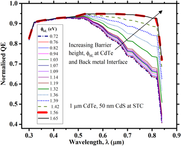
Figure 5. Effect of back metal WF on QE in CdTe solar cell.
Download figure:
Standard image High-resolution imageIn conventional CdTe solar cell, value for VOC ranges typically from 800 mV to 850 mV [19]. Using nanocrystalline CdS window layer, VOC of 1017 mV has been achieved [19]. When PHIBL = 0.72 eV for Ir (210-plane) metal, voltage goes to a maximum at open circuit voltage, VOC of ∼660 mV. From PHIBL of 0.72 eV to 1.65 eV, short circuit current density, JSC increases from 24.6 mA cm−2 to a maximum of 28.6 mA cm−2. However, voltage is dominated mainly by PHIBL. VOC increases rapidly with increasing PHIBL as shown in figures 4 and 5. Although the JSC is found same at 28.6 mA cm−2 for Pt with either (110) or (111) plane, VOC is different. Highest obtained VOC was 1193 mV (∼1.2 V) for Pt back metal at (111) plane. This result shows the possibility of having voltages > 1V without any back surface field (BSF) layer if one incorporates Pt (111) as back metallic contact in CdTe solar cell. Metal Pt can be utilized industrially for higher performances in a large scale production since Pt has lower price compared to usually used Au back metal. This design will lead towards a simple CdTe solar cell structure with high voltages than previously obtained.
Approximately 90% QE can be achieved (figure 5) in most portions of the wavelength range for PHIBL > 1.42 eV i.e., metal WF > 5.7 eV. For 520 nm to 760 nm wavelength range, QE can be as high as 94.8% with Pt back metal at either (110), or (111) plane. Figure 6 reflects the photovoltaic performances with respect to varying PHIBL. It is evident from figure 6 that all output improves with increasing PHIBL i.e., back metals with higher surface work function (Φm). Cell efficiency increases almost linearly with increasing PHIBL. Highest fill factor (FF) and JSC were attained for Platinum (Pt) metal at either (110) or (111) plane. Only Iridium (Ir) at (111) plane can compete the performances gained with Pt metal to some extent. To sum up, Platinum (Pt) at (111) plane has been opted to be used in back metal of our structure which is kept fixed for the subsequent simulation. This can be an optimistic solution for achieving VOC beyond 1 V in single junction CdTe based solar cells.

Figure 6. Effect of barrier height on PV performances for various back metals in CdTe solar cell.
Download figure:
Standard image High-resolution image3.2. Optimization of the p-type CdTe absorber layer
Under STC at cell operating temperature, T of with 20 nm thick n-type CdS window layer and all other parameters being constant, figures 7 and 8 show the results obtained from AMPS-1D when the thickness of the p-type CdTe absorber layer was varied from 0.1 μm (100 nm) to 1.8 μm (1800 nm).

Each incremental thickness of CdTe absorber layer has a tendency of absorbing light. The thicker the absorber, the more prone light will be imbibed into the absorber, and more electron-hole pair to be generated. Figure 7 discloses that the short circuit current density increases sharply from 17.13 mA cm−2 to 27.109 mA cm−2 till 700 nm. Then it becomes almost stable in between 27.3 mA cm−2 and 27.8 mA cm−2 till 1800 nm. Open circuit voltage increases very slowly from 1.181 V to 1.193 V with increasing CdTe layer thickness till 600 nm. Beyond 1100 nm, it remains constant at 1.194 V.


Figure 7. and w.r.t. CdTe layer thickness.


Download figure:
Standard image High-resolution imageFrom figure 8, it is found that greater the thickness of the p-type CdTe layer, higher is the efficiency of the solar cell. Cell efficiency (η) increases rapidly from less than 18% to greater than 29% till 800 nm of the p-type CdTe layer. Then a slight negligible increment is noticed in the efficiency. If we go on increasing the thickness of the CdTe layer from 800 nm to 1800 nm, the efficiency will increase from 29.091% to 29.685%, implying an increase of only 0.594% efficiency by an addition of 1000 nm thick layer. But the cost will increase swiftly because of the two times thickness increment which is very insignificant compared to the level to which the efficiency is increased. Fill factor raises till 400 nm, then becomes constant at a percentage of 89.3. We determined the effect of CdTe thickness on cell performance, presenting that cell opto-electrical performance improves gradually from 0.8 μm to 1.8 μm of CdTe layer.

Figure 8. Efficiency and FF w.r.t. CdTe layer thickness.
Download figure:
Standard image High-resolution imageFinally as a trade-off between cost and performance, 800 nm thick CdTe layer is approved for proposed cell structure which is over hundred times thinner than conventional bulk Silicon wafer based solar cell and two to three times thinner than conventional CdTe TFSC.
3.3. Optimization of the n-type CdS window layer
Under STC at with 800 nm thick p-type CdTe absorber layer and all other parameters being constant, figures 9 and 10 demonstrate the results obtained from AMPS-1D when the thickness of the n-type CdS window layer was varied from 15 nm to 100 nm. It is evident from figure 9 that and decreases insignificantly from 27.53 mA cm−2 to 27.518 mA cm−2 and from 1.193 V to 1.192 V respectively with increasing CdS layer thickness from 15 nm to 100 nm. Thus we can surely state that CdS layer thickness has almost no effect on these two parameters or these optical outputs have a little sensitivity to degradation with increasing CdS layer thickness.


Figure 9. and w.r.t. CdS layer thickness.


Download figure:
Standard image High-resolution imageIn a superstrate CdTe/CdS solar cell, thicker CdS window film causes larger attenuation for photons that need to be absorbed by the active absorber layer. It was shown that negligible photo-generated current is contributed by the CdS layer. CdS thus constitutes a photocurrent loss for the wavelength (λ) ranging from 300–520 nm in spite of having a high optical absorption coefficient of over over this range of λ [23]. The poor photo-response results in lowering hole lifetime and higher recombination rate. Thus, parasitic optical absorption in the CdS layer is the prime photocurrent loss, making it compulsory to lessen the CdS window layer thickness in the CdTe/CdS hetero-junction as far as possible. Figure 10 explicates that increasing the thickness of the CdS layer from 15 nm to 100 nm, η decreases from 29.385% to 28.791%. Increasing CdS thickness has also a negative impact on FF. It decreases from 89.4% to 87.7%. Hence we must chose CdS thickness as less as possible for the window layer.


Figure 10. Efficiency and FF w.r.t. CdS layer thickness.
Download figure:
Standard image High-resolution imageBearing in mind the fabrication difficulties and short circuit effect, 50 nm thick CdS is chosen to act as the n-type heterogeneous partner for 800 nm thick p-type CdTe material.
3.4. Effect of acceptor concentration

Under STC with 800 nm thick CdTe and 50 nm thick CdS layers and all other parameters being constant, figures 11 and 12 illustrate the findings obtained from AMPS-1D simulation when the acceptor ion impurities concentration, in CdTe layer was varied from to Figure 11 shows the effect of on the short circuit current density which increases with the increase of The open circuit voltage was fixed at 1.193 V over the range simulated. Figure 12 shows that cell efficiency (η) increases beyond of Reverse saturation current decreases with increasing doping concentration leading to an increase in the cell conversion efficiency. Higher the doping concentration, more the growth time and deposition cost. Higher concentration of acceptor impurities in CdTe will reduce the density of minorities (electrons in this case). Thus it is sufficient to take for to improve efficiency.


Figure 11. and w.r.t.


Download figure:
Standard image High-resolution image
Figure 12. Efficiency and FF w.r.t.

Download figure:
Standard image High-resolution image3.5. Effect of donor concentration ()

Under STC with 800 nm thick CdTe and 50 nm thick CdS layers and all other parameters being constant, figures 13 and 14 illustrate the findings obtained from AMPS-1D simulation when the donor ion impurities Conc. () was varied from to Figure 13 shows the effect of on which tends to go down with increasing The open circuit voltage was fixed at 1.193 V over the range of simulated. Figure 14 exhibits that η decreases beyond of Higher the doping concentration, more the deposition time and production cost. We investigated from both figures that all the opto-electrical output parameters remain almost constant till of Hence for can be opted for CdS layer in the solar cell.


Figure 13. and w.r.t.


Download figure:
Standard image High-resolution image
Figure 14. Efficiency and FF w.r.t.

Download figure:
Standard image High-resolution image3.6. Effect of operating Temperature on cell PV performance
Solar cell performance degrades from the reference points at the non-optimal operating temperatures. These cells work greatest at certain optimum temperature. All the thin film solar cells lose some percentages of their conversion efficiency with increasing operating temperature. For instance, at normal terrestrial temperatures of silicon's efficiency compares satisfactorily with other materials; but at a high temperature of silicon's efficiency has dropped to 5% [24]. We determined the effect of cell operating temperature, T on cell performance, showing that cell opto-electrical performance ( η, and FF) degrades gradually with increasing temperature, except for the short circuit current which was found to be almost constant. Heat is nothing but the trembling of atoms and molecules on atomic and molecular level. For any solar cell working at a higher temperature implies that the atoms are vibrating quicker, so it's harder for the electron to get out without bumping into these atoms.


When cell operating temperature increases, thermal energy increases accordingly. The lattice vibrations obstruct the route of the free passage of charge carriers, thus the junction begins to lose its power to keep the charges apart. As a result, cell efficiency goes down due to the collision with thermally excited atoms. With 800 nm thick CdTe and 50 nm thick CdS cell at STC, cell efficiency, η was found to be 29.33% with of 27.53 mA cm−2, of 1.193 V, and FF of 89.3%. When the solar cell is heated, open circuit voltage decreases faster than the short circuit current increases, resulting reduction in overall efficiency. Decreasing cell efficiency with increasing temperature of figure 15 explores a negative temperature coefficient of which reveals the value of a highly stabilized solar cell.


Figure 15. Photovoltaic performances w.r.t. cell temperature.
Download figure:
Standard image High-resolution image3.7. Current-voltage characteristics of proposed CdTe solar cell
The current density versus circuit voltage (J-V) characteristic curves of the proposed CdTe solar cell is displayed in figure 16. Under STC, values for the key optoelectrical output parameters of the cell such as short circuit current density open circuit voltage fill factor (FF) and cell power conversion efficiency (η) have also been provided in figure 16. With only 800 nm thick CdTe active absorber layer, our proposed structure promises better quality device than the conventional ones.


Figure 16. J-V curve of the proposed CdTe solar cell.
Download figure:
Standard image High-resolution image4. Conclusion
Numerical simulation and quantitative analysis of MgF2/glass/Sno2: Sb/CdS/CdTe/Metal heterostructure thin-film solar cell has been carried out. The effect of back metal work function, layer thickness, doping concentration, and operating temperature on cell PV performances were studied in details. As an epilogue, 800 nm thick CdTe as the active p-type absorber layer, 50 nm thick CdS as n-type window layer, 100 nm thick (ATO) as n-type front TCO contact with surface work function of 4.5 eV, Platinum (111 plane) having work function of 5.93 eV as back metallic contact have been opted for proposed structure of the solar cell. The optimized doping concentration has been chosen for donor impurities and that for acceptor impurities has been arbitrated At STC, our proposed cell structure offers cell efficiency, η of 29.33% with of 27.53 mA cm−2, FF of 89.3%, of 1.193 V, and temperature coefficient of which doubtlessly hints the possibility of being an efficacious thin-film solar cell.


Acknowledgments
The authors would like to thank Professor Stephen J. Fonash and his team of the Centre for Nanotechnology Education and Utilization of the Pennsylvania State University, USA for supporting them by providing AMPS-1D software package.