

Abstract
The ability to merge electronic devices with biological systems at the cellular scale is an interesting perspective. Potential applications span from investigating the bio-electric signals in excitable (and non-excitable) cells with an insofar-unreached resolution to plan next-generation therapeutic devices. Semiconductor nanowires are well suited for achieving this goal because of their intrinsic size and wide range of possible configurations. However, production of such nanoscale electrodes can be pricey, time-consuming and affected by poor compatibility with the Complementary Metal-Oxide-Semiconductor integrated circuits (CMOS-IC) process standards. To take a step forward, we introduced a new method to fabricate small, high-density Silicon Nanowires (SiNWs) with a fast, relatively inexpensive and low-temperature (200 °C) process compatible with CMOS-IC standards, thus theoretically allowing on-site amplification of bioelectric signals from living cells in tight contact. Here, we report our preliminary data showing the biocompatibility of SiNWs, as a necessary step to produce a compact device providing super-resolved descriptions of bioelectric waveforms captured from the subcellular to the network level.
Export citation and abstract BibTeX RIS
1. Introduction
Nanostructured silicon (ns-Si) is considered with increasing interest for its potential in many different applications within modern electronics [1]; this is mainly related to its optical and electrical properties making it unique when compared with bulk silicon [2–4].
Silicon NanoWires (SiNWs) can be considered as a particular form of ns-Si bearing a quite advantageous property: the well-defined separation between each nanostructure allows for a large increase of their exposed surface. Together, properties of Si and nanostructures, seem very promising to build electronic devices to detect/condition biological signals at high resolution. However, two major requirements need to be fulfilled: (i) the preparation of SiNWs must be compatible with the CMOS-IC process standards; and (ii) SiNWs must be bio-compatible and in tight, structural and functional contact with the living cells.
The growth of NWs is generally obtained by Chemical Vapor Deposition (CVD) on crystalline Si substrates. This technique requires high-temperature. However, low-temperature is key to make the deposition compatible with other materials, such as plastic, glass, or much more complex substrates as integrated circuits (IC). Low-temperature methodology usually requires using metal nanoparticles acting as deposition catalyst, typically gold [5, 6]. Recently efforts have been made to find a valid alternative, as Au induces deep level defects in the Si structure [7], thus making this metal incompatible with the CMOS technology standards. With all this in mind, we chose Sn as catalyst metal for our low-temperature, CMOS IC-compatible method of on-site growth of SiNWs [8].
The ultimate goal of our novel approach is the production of a new-generation, all-electrical array amenable for high-resolution, large throughput recording of biological signals. Efficient coupling between cell membrane and recording electrode is thus a pre-requisite. Patch-clamp, the elective approach for highly resolved recordings from the neuronal network to single-channel level [9], can provide extremely high resolution, though at cost of limited recording throughput and duration. Extracellular recording (e.g. Multi-Electrode Arrays, MEA, and multi-transistor arrays [10, 11]) is less invasive and allow for long-lasting, multiplexed measurements but only with reduced signal resolution. Thus, assembling an all-electrical device for electrophysiological imaging (that is, a closely packed MEA directly connected to a CMOS capable of high-precision recording from a large network of cells) has long been a major focus in bioengineering, yet mostly challenged by the screening of bio-electrical signals [12]. The recent adoption of nanowire transistors and nanotube-coupled transistors connected to CMOS-ICs [13] allowed for recordings with significantly improved signal resolution and represented a relevant step forward in the field. Also, CMOS-based MEAs have been very recently combined to laser opto-poration producing long-lasting recordings with good signal-to-noise ratio [14]. However, the latter technologies are still rather pricey and bear little compatibility between CMOS technology and the nanotechnology required to grow small-sized, packed nanowires on site.
Here, we describe the production of nano-sized, packed SiNWs using a new methodology bearing two points of strength. Firstly, to acquire electrical signals at high resolution we propose the use of an image sensor consisting of a large-scale, high-density and high-sensitivity (6 el s−1) array integrated with CMOS electronics on a single chip [15]. Secondly, to minimize the electrical screening of biological signals we aim at growing Silicon NanoWires (used as nano-detectors) directly onto the ICs, thus providing an extremely tight coupling between the cell membrane and the recording device. Of note, our SiNWs are bio-compatible, as we show here that different cell types can be grown on uncoated substrates bearing nanowires with no alteration of their morphology nor physiology.
2. Methods
2.1. Deposition of silicon nanowires
SiNWs were grown on a Si substrate (floating zone wafer 1 Ω · cm; orientation 〈100〉; 250 μm-thick) by CVD using a vapor-liquid-solid mechanism. The semiconductor wafers were first cleaned with RCA solution (6 parts deionized H2O, 1-part HCl 27% solution, 1-part H2O2 30% solution; 80 °C). At the end of the process, a silicon oxide passivation layer was laid on the silicon surface and in a separate chamber a 5 nm-thick layer of Sn was evaporated onto the silicon oxide layer. To grow SiNWs, the substrate was baked at 400 °C in a vacuum chamber at 1 × 10⁻⁶ mbar pressure under a fast heating regime (3200 °C h−1), so to ensure the formation of very small Sn droplets on the substrate surface. Of note, we intend to substitute the 400 °C baking step adopted insofar with a laser annealing approach to further preserve IC electrodes during the deposition of nanowires. The baking temperature was measured using a thermocouple in contact with the backside of the sample holder (which we will insofar refer to as the 'crucible'). Notably, given the very low thermal mass of Sn droplets compared to the sample plus holder, we assume that the heat transfer from the droplets may be neglected. Thus, the temperature of the substrate along the relatively brief deposition process can be safely considered to be the one indicated at equilibrium by the thermocouple. Following the slow cooling to 200 °C, the sample was exposed for 5 min to plasma in H2 environment at 600 W under a chamber pressure of 2 mbar and a gas flux of 50 sccm.
Last, the sample was processed for 4 min with SiH4 at 300 W (in absence of plasma activation) with a chamber pressure of 2 mbar, substrate temperature 200 °C, and a gas flux of 15 sccm.
2.2. The deposition chamber
The deposition chamber (figure 1) consists of a cylindrical tube allowing for the propagation of only the first TE10 mode of the microwaves field generated by a magnetron at 2.5 GHz and injected into the chamber by an antenna structure. A quartz disc allows for the passage of microwaves while ensuring the preservation of high vacuum in the chamber. The bottom of the chamber consists of a sample holder (the crucible, stainless still or graphite), which serves as substrate induction heater and is fed by a 100 KHz power controller.
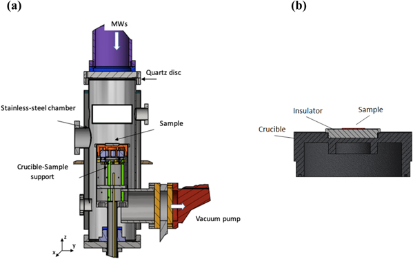
Figure 1. Schematic of the MWCVD deposition chamber (a) and the crucible for substrate heating (b). The sample is located on the crucible sample support bearing a dielectric spacer between the droplet layer and the conductive plane. Because of the tangential electric field concentrated on the sample, Sn droplets are heated up by MWs and work as nano-susceptors at low substrate temperature (Patent Sapienza No: IT0549-17).
Download figure:
Standard image High-resolution imageThe position of the crucible can be controlled on the z-axis so to adjust the waveguide conditions. A dielectric spacer is positioned between the surface of the crucible and the sample substrate both to damp the intensity of the tangential electric field of the microwaves and to avoid energy dissipation onto the conducting crucible, rather than onto the Si surface.
SiNWs are grown as the result of heating the Si substrate in presence of a thin metal layer: the metal droplets formed do function as nano-susceptors of nanowires which in turn build-up in presence of inflowing silane once the eutectic temperature is overcome. Thanks to the MW irradiation Sn nano-susceptors trigger the VLS reaction to grow SiNWs even in presence of a limited percentage of SiH4 and a relatively low substrate temperature (200 °C).
The procedure described leads to the deposition on the silicon substrate of SiNWs with the desired size (typically ∼30 nm diameter) and spacing, within some variability (figure 2).
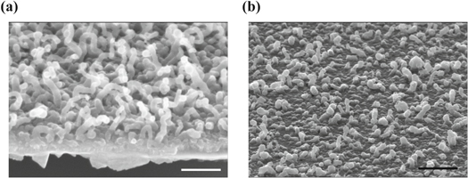
Figure 2. SEM images of typical SiNWs with cross section ∼20 nm ((a), silicon; (b), silicon oxide) grown by the MWCVD method and used as substrates for cell cultures and physiological recordings. Note the Sn droplets still evident at the nanowire tip. Scale bar: 100 nm.
Download figure:
Standard image High-resolution image2.3. Cell cultures, patch-clamp and Ca2+ imaging
2.3.1. Cell cultures
NG108CC15 cells ('NG cells'; hybrid from mouse neuroblastoma N18TG2 and rat glioma C6BUI cells) were grown in standard conditions (37 °C; 5% CO2) using DMEM supplemented with 10% FBS, 100 U ml−1 penicillin, 0.1 mg ml−1 streptomycin (P/S), 100 μM Hypoxanthine, 10 μM Aminopterin, and 16 μM Thymidine. NG cells grown in such non-differentiating conditions appeared relatively depolarized and void of mature action potentials, as expected [16]. BV-2 microglial line cells were grown in 10% FBS, 1% P/S DMEM. All cells were plated on uncoated substrates (glass coverslips or SiNWs) and used 24–48 h after seeding.
2.3.2. Patch-clamp and Ca2+ imaging
For patch-clamp, cells were bathed with standard external solution containing (in mM): 145 NaCl, 2 CaCl2, 1 or 2 MgCl2, 4 KCl, 5 HEPES, 5 glucose, 2 Na-pyruvate (pH 7.4, NaOH). The intracellular pipette solution contained (in mM): 110 K-gluconate, 12 KCl, 10 Na2-Phosphocreatine, 10 HEPES, 0.1 EGTA, 4 Mg-ATP, 0.3 Na-GTP (pH 7.3, KOH; 295 mosm, adjusted with sucrose). The open-tip resistance of borosilicate pipettes ranged from 4.5 to 9.5 MΩ prior to 30∼60% compensation. Due to the substrate opacity to transmitted light, cells on engineered substrates were visualized using IR-DIC optics (Leica DM LFS); recordings were acquired using pClamp9 controlling a MultiClamp 700B amplifier (Molecular Devices). In current-clamp experiments, to describe the passive and active properties of NG cells we applied a family of current steps (Iinj –200 to +600 pA, 50 pA increments, 1s-long; inter-sweep-interval 1.5 s; HP –80 mV). Cell input resistance (Rin) was calculated as the slope of the linear least-squares fit to the voltage–steady state current relationship corresponding to the first four hyperpolarizing steps. Voltage-sag was estimated as the average percentage decrease of the ∣Vm∣ at the steady-state versus peak response to the first three hyperpolarizing steps [17]. For voltage-clamp experiments, to investigate the expression of voltage-activated Inwardly Rectifying (IR) or Outwardly Rectifying (OR) K+ channels BV-2 cells were challenged with a family of voltage steps (Vcmd –130 to +30 mV, 1-sec long, 20 mV/step, inter-sweep-interval 5 s; HP –70 mV). The current density was calculated as current/whole-cell capacitance, the latter being estimated using the amplifier compensation circuit.
For Ca2+ imaging, cells were loaded with the Ca2+-sensitive fluorescent dye Fura-2 (cell permeant, 2 μM; 45 min at 37 °C) and recordings were performed in standard external solution (above). Control or agonist (1 mM ATP, 3-sec long application) solutions were delivered by independent tubes positioned 50–100 μm away from the cell and connected to a fast exchanger system (RSC 100, Biologic). Epifluorescence acquisition was driven by Axon Imaging Workbench software (Molecular Devices; 380 nm exc. and 510 nm em. wavelength). All recordings were at room temperature.
3. Results
3.1. Characterization of resulting silicon nanowires
The structures we produced are a dense network of individual SiNWs. After SEM characterization, providing information about morphological features of the analyzed samples, a characterization of crystallographic structure and surface chemistry was performed respectively by XRD and XPS analysis. For this analysis the two SEM images of the chosen samples (insofar refer to as sample A and sample B) are reported in figure 3.
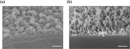
Figure 3. Silicon NWs on samples (A) and (B). The two samples ((a) and (b), respectively) were grown with different deposition parameters. Scale bar: 100 nm.
Download figure:
Standard image High-resolution imageIn figure 4(a) the diffraction patterns of the silicon wafer (reference) and that of the two samples, respectively A and B, are reported. In addition to the peak (400) at 69° related to the crystalline substrate of the three samples, the diffraction patterns show one/two weak peaks that can be attributed to a metastable BC8-structured silicon phase (Si-III, Spatial group Ia-3, ICSD code 16955 and 246372). The absence of other peaks proves the highly oriented growth of the nanostructures.
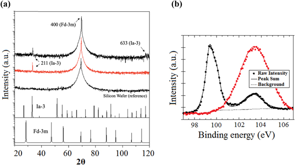
Figure 4. Characterization of crystallographic structure and surface chemistry of SiNWs. (a), XRD measured diffraction pattern of sample A (black), sample B (red) and silicon wafer, as reference. Below, the simulated pattern of cubic diamond Si-I respectively with Ia-3 and Fd-3m structure. (b), XPS Si2p band for both samples recorded in high-resolution mode.
Download figure:
Standard image High-resolution imageUsually, at ambient pressure silicon is found in different allotropes: the most stable cubic diamond silicon (Si-I, Spatial Group Fd-3m) and two metastable forms (BC8-structured Si-III and R8-structured Si-XII), usually obtained by decompressing the high-pressure phase β Sn structured Si-II). In particular, the BC8-Si (discovered in 1963 by Wentorf and Kasper [18]) bears a cubic structure with one crystallographic unique silicon atom resulting in a direct band gap semiconductor. Among its many characteristics, the low gap (30 meV) is particularly useful for the realization of good contacts [19].
To better evaluate the structural composition of our SiNWs, we paralleled our XRD study with an XPS analysis (figure 4(b)). This approach showed for sample A the presence of a Si2p signal formed by the overlap of two different components, centered at different BE (black trace in the plot). The two components are well resolved, suggesting that the sample is very homogeneous in the analyzed thickness. The relative amount of the two chemical species of Si are 70% (Si) and 30% (SiO2); the presence of SiO2 is in agreement with both the BE of O1s band (533.0 eV, FWHM = 1.8 eV; table 1). For sample B, the ratio between oxygen and silicon appeared definitely lower than 2, suggesting the presence of sub-stoichiometric silicon oxide too, SiOx (x < 2).
Table 1. Atomic fraction of Si, O, C, and N as obtained by XPS data (Si value normalized to 100).
| Specie | Sample A | Sample B |
|---|---|---|
| Si | 100 | 100 |
| O | 73 | 154 |
| C | 37 | 36 |
| N | — | 18 |
With regards to the XRD/XPS data, its worth commenting that, along the nanowire surface, silicon faces with different crystallographic orientation may be exposed, thus offering different possible bonding with oxygen atoms. The distinct XPS profile of the two samples analyzed related to their different nanostructure: as shown in figure 3, the surface structure of sample A is characterized by droplets around 50 nm in diameter, whilst sample B exhibits nanowires of 10 nm in diameter. As the air exposure promotes the silicon oxidation of deposited nanowires, the thinner ones (sample B) are predictably completely oxidized, whilst the thicker ones (sample A) are oxidized reasonably only in the outer shell, leaving unaffected the metallic silicon core. Last, the rough structure of sample B might explain an inhomogeneous surface charging, being the tip of the nanowire very far off the conductive substrate.
3.2. Study of silicon nanowires bio-compatibility
Once obtained Silicon NWs using an IC-compatible low-temperature process and provided their chemical and crystallographic surface characterization, we stepped onto testing their biocompatibility. Keeping in mind the possible application of our engineered substrates as components for both high-resolution recording devices and conditioning prosthetic implants, we chose to investigate the effects of SiNWs on neuronal and microglial cells.
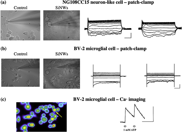
Thus, we performed patch-clamp experiments on NG108CC15 cells, a hybrid cell line showing some neuronal properties [16]; and BV-2 cells, a murine cell line commonly chosen to model native microglia [20, 21]. We also tested SiNWs for biocompatibility using primary cultures from neonatal mice and verified that both hippocampal neurons and microglial cells could be grown on SiNWs with no alteration of their morphology (immunofluorescence preliminary data; not shown). Notably, all cell types tested were successfully grown on engineered substrates. In particular, in current-clamp experiments we found that in response to the injection of hyperpolarizing and depolarizing current steps NG108CC15 cells had both passive properties (resting membrane potential; membrane capacitance; voltage sag and input resistance; not shown) and active response (firing profile) unaltered by the presence of SiNWs as seeding substrate (figure 5(a)). Likewise, when investigating BV-2 cells in voltage-clamp experiments to test for their membrane expression of voltage-activated IR or OR K+ channels [22], we found no difference across seeding conditions (figure 5(b); for patch-clamp experiments, n = 3-to-4 cells per condition; p > 0.3 or more, unpaired t-test when applicable). To further demonstrate that cells grown on SiNWs do express a pattern of membrane receptors similar to those present in physiological conditions we performed Ca2+ imaging experiments on BV-2 cells on SiNWs and found that both basal intracellular [Ca2+] and 1 mM ATP-elicited [Ca2+]− rise were typical of these cells in normal culture conditions (figure 5(c)) [23]. Altogether, our preliminary investigations indicate that SiNWs do not alter normal survival and basic properties of both microglial and neuronal cells in vitro thus resulting amenable for non-interfered biological measures.
Figure 5. Patch-clamp recording and Ca2+ imaging experiments from cells in culture on uncoated glass coverslips (Control) or silicon nanowires (SiNWs), as indicated. (a), current-clamp experiments on NG108CC15 cells. Cells show i) unaltered morphology under IR-DIC visualization (left panels); ii) similar firing profile typical of NG cells kept in non-differentiating culture condition (i.e., lack of spike trains in response to depolarizing injected currents; right panels). (b), voltage-clamp experiments on BV-2 cells. Panels depict lack of difference across seeding substrates for both cell morphology (left) and array of voltage-gated K+ channels expressed (right). Note that transmitted light images captured in presence of SiNWs appear blurry due to the optical properties of silicon substrates. Scale bars: current-clamp, 100 ms, 20 mV; voltage-clamp, 200 ms, 200 pA. (c), Ca2+ imaging experiments from BV-2 cells in culture on SiNWs. Left, typical optic field depicting fura-2 AM loaded cells. The arrow indicates a cell responsive to the fast application of 1 mM ATP. Right, time course of the fluorescence response (indicating [Ca2+i] rise) to two consecutive applications of ATP (arrows). Typically, we found three-to-four responsive cells per optical field (6 fields analysed across different substrates, no difference found). Bars: fluorescence ratio 0.05; 100 s.
Download figure:
Standard image High-resolution image
4. Conclusions
In this work we described a novel technology for the fabrication of small, high-density Silicon NanoWires, and demonstrate that this material is amenable for cell culturing.
We have shown the possibility to deposit a variety of different nanostructures at low temperature using microwaves to heat merely the small droplets of metal catalyzer. This new technique is compatible with CMOS technology and could ideally be used to grow nanowires directly on the back-end of ICs. If proved, such approach would let us couple the enormous sensitivity of silicon nanowires and nanostructures with the vast elaboration capability of the electronic integrated circuits.
Using XPS analysis we showed that, beside different conformation, our silicon nanostructures also bear different crystallographic structure, which can be discriminated by during the deposition process simply adopting different experimental conditions. In particular, we found that by providing higher energy the deposited material appears as cubic diamond silicon; in contrast, with lower energy we found evidence for BC8-Si, a highly-conductive crystal configuration usually difficult to obtain and yet potentially relevant to develop integrated sensors. Also, the chemical analysis of the surface of samples with SiNWs showed high reactivity, clearly depending on the shape of the silicon structures.
Notably, we demonstrated that SiNWs are neutral to living cells and thus potentially amenable to pass electric signals both from and onto cells in tight contact. We are now testing such potential, aiming to produce a compact, all- electrical device for highly resolved cell recording/conditioning.