

Abstract
In the present work, we investigated the elemental composition, structural and electrical properties of Cu2SnS3 (CTS) ternary semiconductor synthesized by the pyrolytic decomposition of the precursors in vacuum. The molar ratio of Sn/Cu in the precursor solution was varied from 0.2 to 0.6. The x-ray diffraction and Raman analyses confirmed that the synthesized samples mainly consist of tetragonal CTS phase with space group  The dependence of the conductivity of CTS samples on temperature was investigated in the temperature range 10-300 K. A crossover between nearest-neighbor hopping and Mott variable-range hopping conduction mechanisms were observed at
  Analysis of the data yielded the values of the relative acceptor concentration
  with the critical concentration of the metal–insulator transition (MIT)
  cm−3, the localization radius
  with the Bohr radius
  the dielectric permittivity far from the MIT κ0 = 10.7, the mean acceptor energy
  meV and the mean density of the localized states
  meV−1cm−3.
Export citation and abstract BibTeX RIS
1. Introduction
The ternary compound Cu2SnS3 (CTS) is one of the promising candidates as an absorbent layer of solar cells, due to its environmentally friendly elemental composition, low cost and prevalence in nature, as well as their suitable optoelectronic properties. Many studies have shown that Cu2SnS3 is a p-type semiconductor that crystallizes in different syngonies (tetragonal, cubic, monoclinic, triclinic) [1–5]. The band gap of CTS has been reported to be in the range of 0.93-1.51 eV, depending on its crystal structure [1–3, 6, 7]. This value lie in an optimal region for photovoltaic application [8]. Also, optical measurements have shown that all the CTS thin films have a large absorption coefficient exceeding 105 cm−1 [9, 10]. Experimentally, the hole mobility of CTS has been measured to be between 1 and 80 cm2 V−1s−1, and the hole concentration is be about 1018 cm−3 [2]. Most recently, the thin film cells based on the pure CTS fabricated by sulfurization from NaF/Cu/Sn stacked precursor have achieved the record conversion efficiency of 4.63% [11].
During the synthesis of CTS, there is a number of problems that resolving them might increase the photoelectric conversion efficiency. One of them is the considerable deviation from the stoichiometric ration (Cu-rich, Sn-poor, S-loss, etc), that may lead to an increment in defect concentration. Non-stoichiometric ratio also suggests the formation of undesired secondary phases. Thus, by studying the effect of various parameters of the preparation of CTS samples, including various Sn/Cu ratios on their physical characteristics, the photoelectric conversion efficiency of solar cells based on them can be improved. In this work, we investigated the influence of molar ratio of Sn/Cu on the phase composition, structural and electrical properties of CTS samples prepared by the thermal decomposition method. Our work was also focused on the hopping conductivity of all samples to determine a series of important parameters, including the width of the impurity band, as well as the concentration, the localization radius of charge carriers, the dielectric permittivity and the density of the localized states at the Fermi level.
2. Experimental details
2.1. Sample preparation
The synthesis of CTS samples was carried out by pyrolytic decomposition method. The essence of this method is the formation of new compounds by the decomposition of corresponding salts at elevated temperatures. The aqueous solution (a mixture of water and methanol) contains the precursors of CTS samples such as copper chloride (CuCl2·2H2O) for the copper, tin chloride (SnCl2·2H2O) for the tin and thiourea (CS(NH2)2) for the sulfur. It can be seen that the molar ratio of sulfur to metals S/(Cu + Sn) in CTS formula is 1, but due to the fact that elemental sulfur can be easily evaporated at high temperatures, the amount of sulfur in all samples was chosen twice as much as the stoichiometric requirement. After a slow drying process at 75 °C, the obtained powder was pulverized in a mortar and annealed in a vacuum tube furnace at 400 °C for half an hour. To study the effect of the varying molar ratio of Sn/Cu on the formation and characteristic properties of CTS samples, the molar ratio of Sn/Cu was chosen to be 0.2, 0.4, 0.5 and 0.6 for samples (CTS1), (CTS2), (CTS3) and (CTS4), respectively.
2.2. Sample characterization
The chemical composition of the obtained materials was studied using energy dispersive x-ray spectroscopy. The structure and phase composition of the obtained material were determined by x-ray diffraction using Rigaku Ultima IV diffractometer (Japan) with a Cu-Kα source (wavelength λ = 1.54056 Å), without a monochromator, with detector in the range of 2θ = 10–95 deg. in increments of 2θ = 0.02 deg. and scanning speed 2 deg. per minute. Although x-ray diffraction has been widely used as a powerful tool to determine the structure of CTS sample, it could not resolve completely the different phases with similar structures that may be present. Also, the presence of defects may affect the position of the peaks in the diffraction pattern. Furthermore, an additional structure characterization was done by the Raman microscope XploRA ONE with an excitation wavelength of 532 nm (2.34 eV).
In order to study the conductivity of all CTS samples, the obtained powders were pressed into pellets with a parallelepiped shape under a pressure of 0.4 MPa using a laboratory hydraulic press PLG-20. Then the pellets were additionally annealed at a temperature of 200 °C for half an hour. The temperature dependence of electrical resistivity was measured by the standard six probe technique using the Janis CCS-350S cryostat, the 8200 helium Compressor, LakeShore Model 331 Temperature Controller and the Agilent Digital Multimeter. The contacts were made with a silver paste. The resistivity measurements were performed in the temperature range of 10-300 K with a step of 2 K and recorded by Labview program.
3. Results and discussion
3.1. Structural study of the CZTS samples
The elemental composition of all the CTS samples obtained using energy dispersive x-ray spectroscopy (EDS) is shown in table 1. From table 1 it is seen that even though the amount of sulfur (S) in the precursors was twice as much as stoichiometric requirement, sulfur deficiency was observed in all synthesized samples. In addition, it is worth mentioning that the loss of tin (Sn) during the high-temperature annealing process was also observed. This fact was found to be in accordance with references [2, 9]. The elemental composition analysis showed that CTS4 is probably the best sample, since it was found to have near-stoichiometric composition. Considerable deviation from the stoichiometry of other samples suggests the presence of unwanted phases.
Table 1. Element composition of all the Cu2SnS3 samples based on energy dispersive x-ray analysis.
| Sample | Molar ratio in the precursor | Composition of elements (in at%) | Molar ratio measured by EDS | ||||
|---|---|---|---|---|---|---|---|
| Sn/Cu | S/(Cu + Sn) | Cu (%) | Sn (%) | S (%) | Sn/Cu | S/(Cu + Sn) | |
| CTS1 | 0.2 | 1 | 52.92 | 9.13 | 37.95 | 0.17 | 0.61 |
| CTS2 | 0.4 | 1 | 42.27 | 14.23 | 43.50 | 0.34 | 0.77 |
| CTS3 | 0.5 | 1 | 42.22 | 17.21 | 40.57 | 0.41 | 0.68 |
| CTS4 | 0.6 | 1 | 38.13 | 18.69 | 43.18 | 0.49 | 0.76 |
Figure 1 shows the powder x-ray diffraction patterns of the studied samples with different molar ratios of Sn/Cu. The structure and the cell parameters of the synthesized samples were determined by the Rietveld method using the FULLPROF program [12]. The diffraction data refinement showed that the compounds crystallized in a tetragonal structure with symmetry  Results from x-ray diffraction analysis revealed that the CTS2, CTS3, CTS4 samples were single-phase. At the same time, the presence of a secondary phase Cu2S with space group
  had found in the CTS1 sample. Although the presence of a secondary phase in the sample (CTS1) was undesirable, but not surprising, since copper-rich growth conditions may promote the formation of different copper sulfide [13]. The lattice parameters and average crystallite size of the CTS compounds determined by x-ray diffraction analysis are shown in table 2.
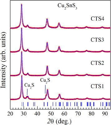
Figure 1. Powder diffraction patterns of the CTS1-CTS4 samples.
Download figure:
Standard image High-resolution imageTable 2. Lattice constants and crystallite size of the CTS samples.
| Sample | а(Å) | с(Å) | Crystallite size (Å) |
|---|---|---|---|
| CTS1 | 5.396 | 10.885 | 74.79(3) |
| CTS2 | 5.416 | 10.922 | 69.85(3) |
| CTS3 | 5.423 | 10.937 | 75.60(6) |
| CTS4 | 5.427 | 10.943 | 60.46(9) |
The average crystallite size in table 2 was calculated using the Debye–Scherrer equation:

where D is the crystallite size in angstroms; n is a dimensionless shape factor, with a value close to unity; λ is the wavelength of x-ray radiation in angstroms; β is the line broadening at half the maximum intensity; θ is the Bragg angle in radians [14]. It can be seen from table 2 that with variation of the molar ratio Cu/Sn from 0.2 to 0.6, the average crystallite size ranges from 75.60 Å to 60.46 Å.
Raman spectroscopy is a useful complementary technique to analyze the phase composition of the obtained samples. Raman scattering spectra of all the CST 1, 2, 3 and 4 samples are shown in figures 2(a)–(d), respectively. Three peaks at 296 cm−1, 336 cm−1 and 351 cm−1 presented in the Raman spectrum of all four samples are attributed to tetragonal CTS phase [15–17]. On the other hand, the peak at 231 cm−1 indicates the presence of Sn2S3 phase in CTS1, CTS2 and CTS4 samples [18]. The peak at 160 cm−1 observed in the Raman spectrum of the CTS3 sample is attributed to SnS phase [17]. In agreement with x-ray diffraction analysis and the reported Raman data in literature [16, 17], the peak at 468 cm−1 in CTS1 sample is assigned to Cu2S phase. Thus, the peaks corresponding to the tetragonal CTS phase were observed in all four samples in the Raman scattering spectra. However, the samples were found to contain SnS, Sn2S3 and Cu2S as secondary phases along with tetragonal CTS. The absence of secondary phases (excluding Cu2S) in the x-ray diffraction pattern could be due to the following two reasons: first, the amount of the secondary phase in the samples was too small to be determined by x-ray diffraction. Second, the secondary phase might be present in amorphous form. In conclusion, by using x-ray diffraction and Raman spectroscopy, it could be confirmed that the synthesized samples mainly consist of tetragonal CTS phase.
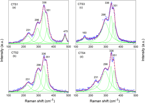
Figure 2. Raman spectra of CTS samples with indication of the characteristic peaks.
Download figure:
Standard image High-resolution image3.2. Investigation of electrical conduction mechanisms of CTS samples
The resistivity measurements of CTS samples were performed in the temperature range of 10 to 300 K. In general, the conductivity increases with rising temperature indicating the semi-conductive behavior of all obtained samples. Figure 3(a) exhibits the variation of resistivity of CTS samples with the inverse of absolute temperature. The observed increase in electrical resistivity with an increment in the Sn/Cu molar ratio from 0.2 to 0.6 (except the CTS3 sample) could be associated with a decrease in the crystallite size (table 2) and with copper-poor conditions in the samples. Similar observations have been reported in literature [19–21]. According to [19–21] in polycrystalline semiconductors, the electrical resistivity of samples increases with a decrease in the crystallite size due to a decrease in charge carrier mobility. Furthermore, from figure 3 it was observed that two regions with different slopes in the plot suggest the presence of two different conduction mechanisms in the investigated temperature range.

Figure 3. (a) The plot of  versus 1/T for the CTS samples. (b) The plot of
  versus T-1/4 for investigated samples CTS1-CTS4. The straight lines are linear fit. For convenience the plots for sample CTS3 are shifted by +0.26 and +0.5 units along the vertical axis.
Download figure:
Standard image High-resolution imageThe conduction mechanism of CTS samples at high temperatures was obtained by fitting the experimental data to the following universal equation [22]:

where ρ0 is a pre-exponential factor, Eact is the conductivity activation energy and kB is the Boltzmann constant. The variation of resistivity ρ in the high-temperature region can be explained by considering three possible types of conduction mechanism: activation of the main carriers from the level formed by defects to the valence band; excitation through the 'mobility edge' in non-delocalized (extended) states and nearest-neighbor hopping (NNH) [22]. The basic difference between the band and NNH conductions is essentially that the pre-exponential factor ρ0 does not depend on temperature in the first case, while in the second case  where A is a proportionality constant independent of temperature. Using equation (2), activation energy values of the band (NNH) conduction can be estimated from the slopes of
  versus (1/T) and
  versus (1/T). If the thermodynamic energy of the system is estimated as
  in the temperature range of 150-300 K, it will take values from 13 meV to 25 meV. The activation energies estimated from the linearization of
  versus (1/T) in the case of band conduction were found not to exceed 9 meV, which were too small compared to the thermodynamic energy of the system. Thus, the electrical conduction mechanism of CTS samples at high temperatures more likely obeys the NNH model.
In the low-temperature region, the carrier conduction of studied samples is due to a hopping mechanism. In this case, the temperature dependence of semiconductor resistivity is described by the following relation [23]:

where Ap is a constant pre-exponential factor, T0p is the characteristic temperature depending on the hopping mechanism; a pair of constants p and m determines the type of hopping conductivity. Hopping over nearest-neighbors conductivity corresponds to the value of p = 1, while the variable range hopping (VRH) conductivity governed by the Mott and Shklovskii–Efros mechanisms are characterized by p = 1/4 and p = 1/2, respectively. The values of p and m corresponding to the various mechanisms of hopping conductivity are given in table 2 in [23].
In our work, the hopping conductivity mechanism of investigated samples in the low-temperature region was determined by analysis of the local activation energy Eloc given by the following equation [22, 23]:

Then equation (4) can be presented in the form:

The left-hand side of equation (5) represents a linear function of  for a single value of m. The value of p can be found from the slope of this plot. Therefore, the determination of hopping conductivity mechanism is carried out as follows: the dependence of
 ![$\mathrm{ln}\left[{E}_{loc}/\left({k}_{B}T\right)+m\right]$](https://content.cld.iop.org/journals/2053-1591/6/5/055915/revision2/mrxab0775ieqn19.gif) versus
versus  was plotted for fixed values of m. Then the value of p was determined for each value of m, that gives the function of p(m). Using this function, one can choose a proper pair of m and p in agreement with those in [23]. The plot of p(m) for each studied sample was shown in figure 4.
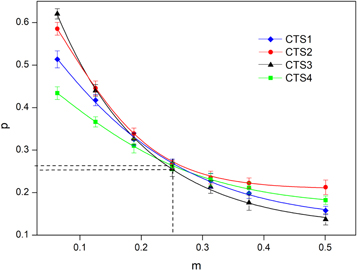
Figure 4. Dependence of p on m for CTS1-CTS4 samples.
Download figure:
Standard image High-resolution imageFrom figure 4, in order to determine the mechanism of conduction, the best fit is obtained using m = 1/4 and p = 1/4 for all samples. As a result, the behavior of the electrical resistivity of the samples CTS 1, 2, 3 and 4 in the low-temperature range corresponds to the Mott mechanism of variable range hopping conductivity. Figure 3(b) shows the plot of  versus T−1/4 of the investigated samples CTS1-CTS4. The linear part of the plots in figure 3(b) yields the value of the characteristic temperature T04 as well as the upper limit of the Mott VRH conductivity regime Tv and the lowest temperature Tm, which are listed tin table 3. The dependence of
  versus ln(1/T) for all samples was shown in figure 5. It can be seen from figure 5 that the data plots can be fitted to a linear relationship, giving p = 1/4. In addition, such plots yield the temperature intervals (Tv, Tm), which are close to the corresponding characteristic parameters in table 3.
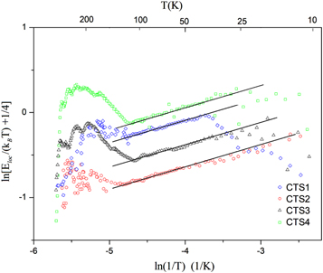
Figure 5.
 versus ln(1/T) for samples CTS1-4. Solid lines the liner fit with a fixed slope of 1/4.
Download figure:
Standard image High-resolution imageTable 3. The onset (TV) and lowest temperature (Tm) of Mott VRH conduction regime, the Mott characteristic temperature (T04), the width of the acceptor band (W), the relative acceptor concentration (N/NC), the relative values of the localization radius (a/a0 and a/aB), the mobility edge (EC) and the DOS g(μ) in all investigated samples.
| Sample | TV (K) | Tm (K) | T04 (K) | W (meV) | N/NC | a/a0 | a/aB | EC(meV) | g(μ) (1016meV−1cm−3) |
|---|---|---|---|---|---|---|---|---|---|
| CTS1 | 150 | 35 | 6923 | 16.8 | 0.77 | 4.4 | 3.7 | 12.2 | 1.6 |
| CTS2 | 140 | 15 | 1040 | 10.0 | 0.85 | 6.7 | 6.5 | 8.5 | 3.1 |
| CTS3 | 130 | 25 | 1579 | 10.5 | 0.83 | 5.9 | 6.1 | 8.8 | 2.8 |
| CTS4 | 135 | 20 | 1133 | 9.9 | 0.85 | 6.5 | 6.5 | 8.4 | 3.1 |
The hopping conduction mechanism of the investigated compounds in the temperature intervals (Tv, Tm) was also confirmed by minimizing the percentage of deviation (Dev) given by the equation (6).

where n is the number of experimental data points [24]. Construction of the Dev function at different values of p allows to determine the type of hopping conductivity. With this method, the variation of Dev (%) as a function of the parameter p for all the investigated samples is shown in figure 6. The best value of p is the one which gives a minimum of the percentage deviation of the fitted curve to experimental points ρi. It is clear that the best fits are obtained for the value of p around 1/4. The percentage deviation of the calculated values from the experimental points of CTS1-CTS4 sample was only 0.6%, 1.3%, 2.7% and 3.6%, respectively. The slight percentage deviations indicate that in this temperature range, the electrical conduction mechanism obeys the Mott VRH model. Thus, observed data for the variation of conductivity in the temperature interval of 10–300 K can be explained by amalgamation of two different conduction mechanisms. In the high-temperature region, the conductivity is governed by the NNH model, whereas in the low-temperature range, the conductivity of the samples is described by the Mott VRH conduction mechanism. This crossover from the NNH to the Mott VRH conduction mechanism was also observed in Cu2ZnSnS4 material with tetragonal structure [25, 26].

Figure 6. The percentage of deviation versus p for investigated samples CTS1-CTS4.
Download figure:
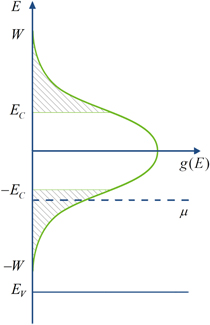
Standard image High-resolution imageThe transition from the NNH to the Mott VRH conduction is often stimulated by increasing the disorder in crystalline structures or lowering the temperature, since this condition is energetically advantageous for the making jumps with end points outside the closest center [22]. On the other hand, the VRH transfer takes place when the Fermi energy, μ, lies in the range of energies where states are localized, and the material is called as 'Fermi glass' [22, 27]. In other words, this material has a finite density of states (DOS), g(μ), around the Fermi level, but in which there is enough disorder for states there to be localized [22, 28]. It means that the Fermi energy lies close to one of the edges of the impurity band (the acceptor band, in our case of the p-type semiconductor). First, this smallness of DOS near the edges of the acceptor band leads to difficulty in finding a closest neighboring site with low activation energy [28]. Second, if the critical energy EC, called the 'mobility edge' separate localized from non-localized (extended) states, the impurity states will be extended in the interval (−EC, EC) around the center of the impurity band and localized outside this interval (see figure 7). If μ lies within intervals of the non-localized states (at −EC < μ < EC) the metallic conduction is expected. Hence, the VRH conduction sets in only for μ lying close to the one of the acceptor band edges. When the Fermi energy crosses the mobility edge (if the density of charge carries or degree of disorder in the system can be varied), that  changes sign, an Anderson 'metal-insulator transition' (MIT) occurs [22, 27].
Figure 7. The DOS versus energy of the acceptor band. The localized states are hatched.
Download figure:
Standard image High-resolution image
Microscopic properties of the localized carries, as well as some important macroscopic parameters of CTS samples were further studied by investigation Mott VRH conduction. The Mott VRH characteristic temperature T04 in equation (3) is determined as ![${T}_{04}=\beta /\left[{k}_{B}g\left(\mu \right){a}^{3}\right],$](https://content.cld.iop.org/journals/2053-1591/6/5/055915/revision2/mrxab0775ieqn25.gif) where
where  is number constant for Mott VRH conduction and a is the localization radius of charge carriers
  [29]. Here, N is the concentration of states involved in the hopping conduction, NC is the critical acceptor concentration of the MIT, a0 is the localization radius far from the MIT [22] (i.e., at
  ) and
) and  is a critical exponent [29].
The linear part of the plot of  versus T1/4 in figure 3(b) yields the value of the characteristic temperature T04, as well as the onset (TV) and the lowest temperature (Tm) of the Mott VRH conduction regime, which are represented in table 3 for all investigated samples CTS1-CTS4. The semi-width of the impurity band, determined from the equation [22]
  is also exhibited in table 3. From table 3, the highest values of T04 and W reflect a strong lattice disorder in CTS1 sample. The near-stoichiometric composition of CTS4 sample might be connected to the reduced value of W and to smaller lattice disorder in this sample. As can be seen in table 3, the CTS3 sample has higher values of T04 and W in comparison with the CST2 and CTS4 samples, it is reasonable to suppose that the secondary phase SnS made the lattice disorder increasing in the CST3 sample. However, the microscopic parameters of sample were not be influenced significantly as the percentage of this secondary phases was very small. The effect of lattice disorder can also be seen from the change in the slope of the
  versus T1/4 plot, as shown in figure 3(b), since the slope is sensitive to the defect concentration in the sample. Note that that the maximum value of slope was obtained for CTS1 sample indicates the largest concentrations of defects. This result is in agreement with the collected data in table 3 and the discussion above.
If the DOS is approximated with the rectangular shape [28, 30, 31],  the values of relative acceptor concentration N/NC then the relative value of localization radius a/a0 will be obtained by the following equation at

The obtained values of  and
and  (table 3) are consistent with the proximity of the investigated samples to MIT. In doped semiconductors
  where
where  is the Bohr radius. They are given with the relations [22]:

where E0 is the energy of the DOS peak in the impurity band, κ0 is the dielectric permittivity far from the MIT, and  is the effective mass of the charge carries [32, 33]. Therefore, the ratio of a/aB can be also calculated as
  [25] by putting
 and using the expression
 ![${E}_{C}\approx W-{V}_{0}^{2}/\left[4\left(z-1\right)J\right],$](https://content.cld.iop.org/journals/2053-1591/6/5/055915/revision2/mrxab0775ieqn43.gif) here
here 
 is the number of nearest neighbors and
  is the overlap integral [22].
  is the half of the average distance between acceptors, where
  the values of N/NC are taken from table IV and NC from the Mott criterion
  J0 is the prefactor
 ![${J}_{0}\approx \displaystyle \frac{{e}^{2}}{{\kappa }_{0}{a}_{B}}\left[\displaystyle \frac{3}{2}\left(1+\displaystyle \frac{R}{{a}_{B}}\right)+\displaystyle \frac{1}{6}{\left(\displaystyle \frac{R}{{a}_{B}}\right)}^{2}\right]$](https://content.cld.iop.org/journals/2053-1591/6/5/055915/revision2/mrxab0775ieqn50.gif) [22]. Therefore, the only unknown parameter to calculate the ratios of a/aB is κ0. But the value of κ0 can be found by fitting the value of a/aB to the data of a/a0 in table 3 with minimizing the standard deviation SD:
[22]. Therefore, the only unknown parameter to calculate the ratios of a/aB is κ0. But the value of κ0 can be found by fitting the value of a/aB to the data of a/a0 in table 3 with minimizing the standard deviation SD:

where n is the number of samples [28, 31].
At first the best fit for all samples (n = 4) yields high values of the standard deviation SD = 0.83. It is noticed that the difference in structure between the CTS1 and the others sample (observed from x-ray diffraction analysis) may lead to the difference in the dielectric permittivity of this material. Hence, in order to increase the fitting quality, we fit a/aB to a/a0 using only data for CTS2, CTS3 and CTS4 samples (n = 3). In this case, the best fit yields κ0 = 10.7 at a much smaller value of SD = 0.14. The obtained values of a/aB are presented in table 3. The values of  and
and  meV are calculated from equation (8). The estimated value of E0 was two times higher than the acceptor energies of 22.9 and 24.8 meV for Cu-poor/S-rich CTS [34], but quite close to the acceptor energies of 43 meV for CuInS2 [35] and was comparable to energies of 50-60 meV for Cu2ZnSnS4 [25, 36], the critical acceptor concentration of the MIT was found to be
  cm−3. A number of studies have shown that CTS material often has hole concentration in the range of 1017−1019 cm−3 [2, 5, 37]. This high level of carrier concentration might lead to an increase in tunneling enhanced recombination within the absorber layer and at the heterojunction interface [38]. Thus, the calculated values of hole concentration for our CTS samples seem to be more suitable for a photovoltaic absorber material. The values of DOS evaluated with the expression
  and EC for all samples are collected in table 3. The obtained values of κ0 = 10.7 is close to the reported value of κ0 = 9.6 in literature [33, 39]. The deviation from these values may be related to an indirect way to determine the value of κ0 and the rectangular approximation of DOS. However, this small deviation still supports the validity of obtained microscopic parameters shown in table 3.
4. Conclusions
In this study, the Cu2SnS3 samples were synthesized by pyrolytic decomposition of the corresponding metal chlorides and thiourea. Elemental composition, structural and electrical properties of the samples were analyzed. The x-ray diffraction analyses confirmed that our synthesized samples are composed mainly of the tetragonal CTS phase, except for the CTS1 sample, an undesired cubic phase Cu2S is still presented. Using Raman scattering techniques, we also detected the presence of minor SnS and Sn2S3 phases. The variation of conductivity in the temperature range of 10 to 300 K in all investigated samples can be explained by a combination of the nearest-neighbor hopping mechanism in the high-temperature region (T > 145 K) and the Mott variable-range hopping mechanism in the temperature range of 15–145 K. The value of width of the acceptor band, the acceptor concentration as well as the localization radius, the Bohr radius of the charge carries were obtained by analyzing data in conditions of the proximity to the metal-insulator transition. The mean acceptor energy and the mean density of the localized states were also calculated. The value of dielectric permittivity far from the MIT κ0 = 10.7 was found to be similar to obtained result in reported literature. The electrical properties were found to be affected by the crystallite size, the elemental and phase compositions of the studied samples. The electrical resistivity increased with a decrease in the crystallite size. The higher degree of the microscopic disorder in CTS1 sample was attributable to high Sn-deficiency condition and a considerable amount of Cu2S cubic phase.