

Abstract
The mechanical, optical, thermoelectric and thermodynamic characteristics of Cesium based bromides are systematically studied using the most comprehensive DFT based Wien2k code for elucidating the energy renewable device applications. The mechanical, thermodynamic and structural stabilities of the studied perovskites are revealed in terms of Born mechanical stability criteria, enthalpy of formation and Goldschmidt's tolerance factor, respectively. The ductile/brittle nature, anisotropy, wave velocity and Debye temperatures are computed to illustrate the mechanical nature. The optical parameters have been found highly sensitive to the exhibited band gap lying within visible energy. The large thermoelectric efficiency has been found that is responsible to exhibit optimum values of the power factors and the thermal conductivity. Furthermore, the specific heat capacity, Hall coefficient, magnetic susceptibility and electron density are also described in detail. Hence, the studied perovskites showing band gap in visible region have been found suitable for commercial applications in Solar cell, optoelectronic and thermoelectric devices.
Export citation and abstract BibTeX RIS
1. Introduction
Perovskites materials (ABX3 structure) have attained the significant attention for the optoelectronic and photovoltaic applications due to their highly flexible BX6 octahedral corner-connected network and tunable chemical properties [1, 2]. In addition to the oxide perovskites (X = O), the bromides and iodides (X = Br or I) based perovskites have gathered a significant attention in the past few years because of maximum absorption of light in visible region, ease of fabrication and low effective masses [3, 4]. The photovoltaic research is mainly focused on the organic (e.g., A = CH3NH3) and inorganic perovskites and their hybrids because of their high optical efficiency. The semiconducting perovskites having band gap in the visible region are considered suitable for solar cell applications [5], for example, lead based perovskites solar cells (PSCs) exhibits a maximum efficiency 20.1% which is comparable with that of the commercial silicon based solar cells [6]. However, limited stability and suppressed efficiency at high temperature are the main issues offering advanced investigations. Hence, the theoretical and experimental studies of the perovskites for observing the physical and chemical properties have attained a substantial prominence [7]. ABX3 (A = Cs, B = Sn, Pb, Ge; X = Cl, Br, I) perovskites are under the main focus of the research interests because they exhibit tunable optical characteristics [8].
Perovskites solar cells (PSCs) have been reported exhibiting 10% conversion efficiency using their hybrids with the bromides [9], which has been reported to enhanced to 19% using iodides [10]. Furthermore, PSCs such as CsSnI3, CsSnBr3, and CsGeBr3 have also been fabricated without using organic components, however, lower conversion efficiencies have been reported [11, 12]. Such inorganic compounds have potential to exhibit the required properties; however, these also have associated octahedral BX6 distortions. The magnitude of such distortions has a marked effect on the exhibited physical properties [2]. The impact of tilting on the nature of the band gap has been very less investigated for halides based perovskites [13, 14]. As an example, CsSnI3 has four distinct polymorphs [15, 16], in which undistorted cubic (Pm m) perovskites structure is stable at high temperature [17], which is transformed to the tetragonal (P4/mbm) structure at the lowered temperature due to the SnI6 octahedral rotation around the easy axis (c-axis). Many halides e.g., CsSnBr3 [18, 19], CsPbBr3 [20], and RbSnBr3 [21] reveal similar type of octahedral rotations.
The CsSnI3 based PSC has conversion efficiency 2.1% of optical energy to electrical energy because Sn oxidation that causes high recombination rate [12]. The use of passivation dopant SnF2 has been found suppressing the recombination rate [22]. Similarly, bromide (Br) substitution improves stability and reduces recombination rates [23]. The carrier density of CsSnI3-xBrxreduces by twice order of magnitude as XBr increases. Brik et al [24] explored simple cubic perovskite structure of CsGeBr3, CsCaBr3, and CsSnBr3 and found these crystals more vulnerable to the impurity substitutions. The calculated band gap for CsGeBr3 has been reported smaller than the experimental one, i.e., 2.32 eV [25]. In contrast, the optical properties of CsSnBr3 depict that nearly zero band gap is exhibited [26], while calculated band gap at the R point has been found as 0.42 eV [27], which has been found consistent with the value computed using GGA. The calculated refractive index has been computed as 2.62 (GGA) and 2.83 (LDA) for CsGeBr3, and 2.55 (GGA) and 2.81 (LDA) for CsSnBr3. Schwarz et al [25] explored pressure dependent structural and optical properties of CsGeBr3 and CsGeCl3 perovskites to elucidate the light absorption characteristics, and at ambient pressures the absorption edgesare extracted as 2.32 eV and 3.67 eV, respectively, with the trigonal distortion in the structure. Increased hydrostatic pressure resulted CsGeBr3band gap red shifted with the rate −0.61 eV GPa−1. Although many reports elaborate the optical characteristics of the studied perovskites, but thermoelectric properties are not discussed in literature.
In this article, Cesium based bromides are investigated to illustrate the thermoelectric and optoelectronic properties. The thermoelectric properties predict a highest figure of merit (∼3.6) and high light absorbing efficiency elucidate their significance for energy storage and renewable energy devices. We have used modified Becke and Johnson potential for computing the most reasonable electronic structures. Hence, high stability of the perovskites and the exhibited best optical and thermoelectric parameters suggest multifunctional applications of both perovskites illustrating the scientific significance of this work.
2. Method of calculations
The density functional theory based full potential linearized augmented plane wave plus local orbital method programmed in Wien2k code [28] has been applied for the results analysis. In this method, a constant potential both in muffin-tin and interstitial regions is considered. The relaxed structures are optimized using PBEsol approximation [29] for finding the lattice constants and bulk moduli at ground state through Murnaghan equations. The convergence of the optimized structures using modified Becke and Johnson potential [30] is done for more clearly distinguishing the electronic states as compared to GGA + U and LDA + U [31], and hence, the computed electronic properties become more consistent with the experiments. Actually application of mBJ potential overcomes the scarcities introduced due to GGA and LDA, because both functional employ different electron density in the muffin-tin region. The basic initial parameters such as Kmax × RMT and angular moment vector Imax are set as 8 and 10, respectively. A K-mesh 20 × 20 × 20 is used for the best convergence. The convergence is announced until a difference reduces than 0.01mRy between two iterations. The Charpin method is used to reveal the elastic parameters using first-order nonlinear differential equations. The thermoelectric behavior is elucidated using classical theory based BoltzTraP code [32], in which the electronic structures, computed using TB-mBJ potential are fed as input.
3. Results and discussion
The CsGeBr3(CGB) and CsSnBr3 (CSB) are optimized for getting the ground state lattice constants and bulk moduli. The optimized energy versus volume plots are presented in the figure 1, while optimized structure is shown as an inset figure. The cubic structure (space group: 221_Pm3m) shows that Ge/Sn atoms are located within the octahedron, while the tetrahedron edges surround Cs atom. The unit cell is formed with the atomic positions Cs (0, 0, 0), Ge/Sn (0.5, 0.5, 0.5) and Br (0.5, 0.5, 0) respectively. The ground state parameters calculated from the optimized plots using Murnaghan equation of states are presented in table 1. The lattice constant increases from CGB to CSB, in contrast, bulk modulus decreases. As the atomic radius of Sn (2.27 Å) is higher than Ge (2.10 Å), therefore, lattice dimensions of Sn based CSB more elongated compared with those in the Ge based CGB, due to this fact, lattice constant improves and bulk modulus decays from CGB to CSB.

Figure 1. The Crystal structure of 1 × 1 × 1 unit cell of CsGeBr3 and CsSnBr3 formatted by using XCrysden software and optimized plots.
Download figure:
Standard image High-resolution imageTable 1. The calculated parameters of CsGeBr3 and CsSnBr3 in cubic phase by using TB-mBJ potential.
| Properties | CsGeBr3 | Others | CsSnBr3 | Others |
|---|---|---|---|---|
| ao(Å) | 5.46 | Exp.5.35a | 5.78 | Exp.5.79b |
| GGA 5.50c, LDA 5.34c | GGA 5.75c, LDA 5.60c | |||
| Bo (GPa) | 27.19 | 22.96 | ||
| Eg (eV), (mBJ) | 2.20 | Exp. 2.32c | 1.72 | Exp. 1.75c |
| GGA 0.53c, LDA 0.0c | GGA 0.32c, LDA 0.0c | |||
| CATEP Code | CASTEP Code | |||
| PBE-GGA 0.56f | GGA 0.42d,PBE-GGA 0.51f | |||
| ε1 (0) | 5.92 | GGA 6.8c | 5.36 | GGA 6.5c |
| n (0) | 2.43 | Exp. 2.31f | 2.31 | GGA 11.6c, LDA 12.9c |
| GGA 2.62c, LDA 2.83c | ||||
| R (0) | 0.175 | 0.157 | GGA 11.5c, LDA 12.3c | |
| C11 | 58.18 | GGA 49.5c, LDA 70.3c | 63.13 | GGA 44.6c, LDA 57c |
| PBE-GGA 48g | PBE-GGA 43.8g | |||
| C12 | 11.70 | GGA 11.6c, LDA 12.9c | 2.88 | GGA 3.9c, LDA 5.5c |
| PBE-GGA 10.8g | PBE-GGA 6.7g | |||
| C44 | 9.27 | GGA 11.5c, LDA 12.3c | 3.31 | GGA 6.5c, LDA 5.5c |
| PBE-GGA 10g | PBE-GGA 5.2g | |||
| B | 27.00 | PBE-GGA 23g | 22.00 | PBE-GGA 19g |
| G | 13.53 | PBE-GGA 12g | 9.58 | PBE-GGA 8.9g |
| Y | 34.83 | PBE-GGA 32g | 25.24 | PBE-GGA 23g |
| B/G | 2.01 | PBE-GGA 1.79g | 2.39 | PBE-GGA 2.1g |
| ϒ | 0.29 | GGA 0.19c, LDA 0.15c | 0.32 | GGA 0.08c, LDA 0.088c |
| PBE-GGA 0.27g | PBE-GGA 0.30g | |||
| A | 0.40 | 0.12 | ||

|
58.09 | 51.37 | ||

|
31.77 | 26.60 | ||

|
35.43 | 29.78 | ||

|
5.50 | 4.41 |
3.1. Thermodynamic, structural and mechanical stability
The experimental realization of studied characteristics needs a comprehensive understanding of the thermodynamic, structural and mechanical stabilities of the perovskites responsible for exhibiting fundamental characteristics. The crystal structure for both perovskites is shown in figure 1. The thermodynamic stability is confirmed because computed enthalpy of formation appears with negative sign [33] as evident in table 1. The structural stability is illustrated by computing Goldschmidt's tolerance factor (tF), which is mathematically shown as  where,
  and
and  are the ionic radii of the cations at the tetrahedral and octahedral sites, respectively. While,
  expresses the ionic radius of the anions surrounding the cations by forming tetrahedron and octahedrons [34]. An ideal perovskite exhibits the unity tolerance factor, and deviations from unity illustrate structural distortion having magnitude proportional to the mismatch between the ionic radii. The CGB has tF = 1.01 and for CSB tF = 0.96 showing stability of the perovskite structures.
The mechanical stability of the cubic perovskites is shown by solving tensor matrix for the first order nonlinear differential equations using Charpin method as employed in Wien2k code. Owing to the exhibited cubic symmetry, the elastic constants C11, C12 and C44 are extracted from the tensor matrix for illustrating the real mechanical properties. For elucidating the mechanical stability, Born stability criteria defined as C11 − C12 > 0, C11 + 2C12 > 0, C44 > 0 and C12 < B < C11is employed [35, 36]. Moreover, bulk modulus is also computed using the expression B = (1/3) (C11 + 2C12), which has been found in good match with that elucidated using energy optimization process that shows accuracy of the presented computations.
As the brittle or ductile character is critical to be observed before the device fabrication, therefore, Poisson's (υ) and Pugh's (B/G) ratios are computed, which exhibit critical limits 0.26 and 1.75, respectively [37]. The values exceeding the critical limits illustrate the ductile characteristics, while brittle character is shown if ratios are lower than the critical values. As evident in table 1, both perovskites exhibit ductile nature, which increases from CGB to CSB. Therefore, both perovskites show increased device reliability because of their high capacity for withstanding the applied pressures and retaining the intrinsic characteristics. The mechanical anisotropy factor is also computed and an anisotropic behavior is apparent because the computed values are less than unity in the crystalline materials (see table 1). Moreover, CSB exhibits more mechanical anisotropy than CGS because its anisotropy factor finds comparatively more unity deviation. The thermodynamic response is illustrated by computing Debye temperature ( ) and specific heat capacity (Cv). The specific heat capacity will be elaborating while describing the thermoelectric properties. Debye temperature is computed using elastic moduli in the relation [38, 39]:

Where kB is Boltzmann constant, h Plank's constant, NA Avogadro number, M shows molar mass, ρ is electronic density and ѵm shows average sound velocity. The average sound velocity contains one longitudinal (ѵI) and two transverse (ѵs) modes and is calculated using the relation (2)
Both types of velocities are elucidated using Navier's equation:


The sound velocity dependent Debye temperature ( ) considerably affects the exhibited physical properties such as melting temperature, phonon heat capacity and elastic constants. Because the value of
  decreases from CGB to CSB, therefore, it illustrates suppressing of the lattice vibrations.
3.2. Optical properties
The study of the optical behavior is critical to describe the potential optoelectronic applications, which are elucidated by interpreting the nature of material response to the incoming radiations resulting in the electronic transitions across the Fermi level from filled valence band to the available states in conduction band. The typical semiconductors are characterized as exhibiting inter-band transitions from valence (VB) to the conduction band (CB), while the intra-band transitions illustrate a significant role in a typical metal. As the inter-band transitions express a sum of all the possible transitions between VB and CB, [40–44], therefore, optical contributions due to the shallow or deep levels lying close to VB/CB or Fermi level, respectively, is considered relatively small due to the direct band gap. The computed band structures for both perovskites are shown in figure 2, and an evident direct band gap occurs at R-point. The dielectric function ε (ω) = ε1 (ω) + iε2 (ω) elucidates well the optical characteristics by computing the material parameters revealing dispersion, polarization and absorption of the incoming energy. The real ε1 (ω) and imaginary ε2 (ω) parts are interrelated through the Kramer–Korong relation [45] and both are employed to compute all other optical parameters using the relations in Refs. [46–48]. All optical parameters computed for both CGB and CSB are plotted versus energy 0–12 eV in figures 3–4(a)–(d).

Figure 2. The band structure plots for (a) CsGeBr3 and (b) CsSnBr3 calculated by TB-mBJ potential.
Download figure:
Standard image High-resolution image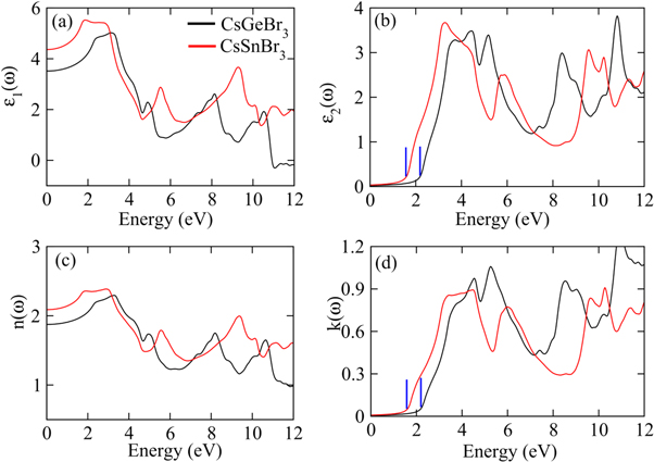
Figure 3. The plots of (a) real part of dielectric constant, (b) imaginary part of dielectric constant, (c) refractive index and (d) reflectivity for CsGeBr3 and CsSnBr3 calculated by TB-mBJ potential.
Download figure:
Standard image High-resolution image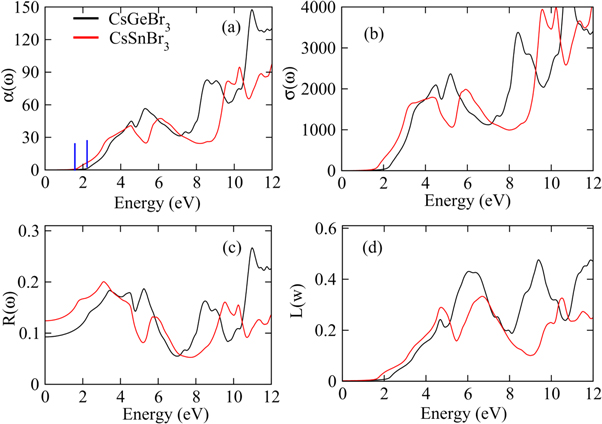
Figure 4. The plots of (a) absorption coefficient, (b) thermal conductivity, (c) reflectivity and (d) energy loss factor for CsGeBr3 and CsSnBr3 calculated by TB-mBJ potential.
Download figure:
Standard image High-resolution imageThe real part of dielectric function ε1 (ω) showing polarization and dispersion of the impinging photons which is plotted for both perovskites in figure 3(a). The ε1(ω) enhances with increasing energy to attain peak value approximately around 2 eV and both compounds exhibit slightly deviating resonance frequencies. The ε1 (ω) decays with further rise in energy and becomes minimum around 6 eV. Moreover, many peaks appearing in ε1 (ω) spectra, observed within 0–12 eV for both perovskites, are due to different inferior resonances frequencies causing deviations from the continuous response. Increasing energy reduces ε1 (ω) spectra, even negative sign is exhibited within 11–12 eV for CGB, which describes the reflection of the impinging photons from the surface that is an illustrative of the metallic nature. Moreover, tuning the incident photonic energy can also result transitions between metallic and non-metallic natures. For estimating a consistency between the computed parameters, the static ε1 (ω) and energy band gap values are contrasted with respect to Penn's relation, ε1(0) ≈ 1 + ( ωp/Eg)2, and values are found in promising agreement [49].
The imaginary dielectric constant ε2(ω), computed for both perovskites is employed to express the energy absorption (see figure 3(b)). The critical of edge values extracted from the ε2(ω) spectra for both CGB and CSB are principally true representative of the exhibited optical band gap, and a good compatibility with the band gap calculated from the band structures has been observed. As the critical energy edge reveal zero absorption for any energy below the threshold limit, therefore, absorption spectra arise above threshold energies and exhibit peak around 4.2 eV for CGB and 3 eV for CSB. A comparatively high and sharp absorption is exhibited by CSB than by CGB (see figure 3(b)). The energy range covering visible and lower part of the ultraviolet part of the electromagnetic spectrum reveals pronounced absorption peaks, which is significant for optoelectronics applications. The computed ε2(ω) drops to 1.3 at nearly 7 eV of CGB and again two maximum peaks appear at 9 eV and 10.8 eV. While, CSB exhibit a minimum absorption at 8.2 eV and again strong absorption is exhibited at 9.6 eV. Hence, such large peaks appearing in the absorption spectra at different energies reveal prominent contributions of the constituent states, as described in the computed band structures, which are responsible for absorbing the specific energies that can allow some electronic transitions. The illustrated strong absorption at the well-defined impinging energies suggests novel energy harvesting applications of the studied perovskites.
The refraction of light elucidates the deviations in the direction of light propagating through any medium, which is inversely linked with the phase velocity variations in the impinging energies. Therefore, the real and imaginary refraction illustrate the transparent and opaque natures and are called as refractive index n(ω) and extinction coefficient k(ω), respectively (see figures 3(c)–(d)). In terms of ε1 (ω) and ε2 (ω), both are expressed as  and
and  The static values n(0) and ε1 (0) exhibit a consistency by obeying the expression
  = n2(0) [47]. The n (0) for both CGB and CSB are extracted as 1.89 and 2.1, respectively, which are suggestive for the optoelectronic applications. Moreover, k(ω) spectra exhibit behavior replicating to that in the ε2 (ω) spectra.
The absorption coefficient α(ω) quantifies the light penetration within the materials before decaying completely. The semiconductor absorption is related with the photons interacting with electrons, because only those photons can excite electrons which have energy exceeding band gap, otherwise transmission occurs. Figure 4(a) shows absorption increasing above the threshold limit (band gap) and approaching to a peak value due to the incoming photons causing electronic transitions. A number of absorption peaks indicate different electronic transitions originating at varying impinging photonic energies. Moreover, α (ω) is sensitive to the incident wavelength and is related with k(ω) i.e.,  The ratio of α (ω) and k (ω) is of the order of wave vector, and hence, increasing wave-vector illustrates improving absorption at the shorter wavelengths.
As the absorption of photon causes free carriers generation, therefore, the computation of optical conductivity expressing the number of free carriers available for the conduction becomes interesting to study. As shown in figure 4(b), optical conductivity increases due to increasing photon energy because more electrons move to the conduction band. Moreover, the edge points after which linearly increasing optical conductivity is evident, are also related with the calculated band gaps of 2.20 eV and 1.72 eV for CGB and CSB, respectively, and hence, verifies that only those photons are absorbed those have energy exceeding the band gap for causing the electronic conduction. The maximum peak appearing within 4.5–6.0 eV and 8.0–12 eV, illustrate that maximum optical conductivity is exhibited due to the higher absorption, because absorption coefficient (see figure 4(a)) exhibit maximum values in these energy range. Interestingly, maximum peak is shifted towards higher energy as the cation changes from Sn to Ge.
The reflectivity, which is a ratio of the reflected to incident energy reveals surface information and evaluates the material for optical device applications. As shown in figure 5(c), the maximum reflection is exhibited within 3.0–5.0 eV and 8.0–12 eV for both CGB and CSB. Moreover, the reflectivity plot exhibits a variety of peaks with the increasing energy revealing potential shielding applications of both perovskites for the photons of varying energies. The incident electron energy loss due to collisions or scattering is described in terms of the energy loss factor L( ), as shown in figure 5(d). It is apparent that L (
 ) shows negligible values up to 2.3 eV, while it increases with energy for exhibiting a maximum at 6 eV. Hence, both perovskites can operate well for the optical applications in the visible and ultraviolet energy regions, as L (
 ) remains minimum for these energies. Consequently, the highest absorption and suppressed L (
 ), for the visible and ultraviolet energy ranges evidence the potential commercial consumption of both perovskites in the fabrication of novel devices involving energy harvesting applications.
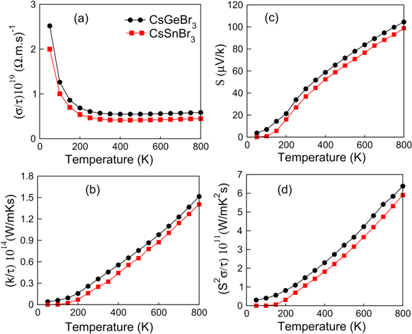
Figure 5. (a) Electrical conductivity, (b) thermal conductivity, (c) See-back coefficient and (d) power factor are plotted against temperature for CsGeBr3 and CsSnBr3.
Download figure:
Standard image High-resolution image3.3. Thermoelectric properties
As the available energy sources are declining across the globe, therefore, addressing of such a gap is a principal challenge for the modern scientific community. The perovskites materials are considered best for commercial applications in the electric generators, refrigerators and thermocouples because of the high electrical to thermal conductivity ratio according to Weidman-Franz law [50]. Therefore, for enhancing the figure of merit ZT = S2Tσ/k and the power factor PF = S2σ, high electrical conductivity (σ), Seebeck coefficient (S) and low thermal conductivity (k) are required [46, 47, 51, 52]. All these parameters are computed and plotted against temperature (0–800 K) in figures 5(a)–(d) and againest chemical potential in figures 6(a)–(d).
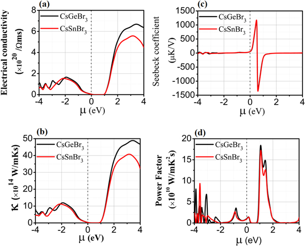
Figure 6. (a) Electrical conductivity, (b) thermal conductivity, (c) See-back coefficient and (d) power factor are plotted against chemical potential for CsGeBr3 and CsSnBr3.
Download figure:
Standard image High-resolution imageThe chemical potential for the electrons represent the change in free energy required to add or remove the electrons from the system by doing work against the electrostatic coulomb repulsion. It is represented as the energy per electrons for the atomic particles rather than compounds and has the units of energy (eV). In semiconductor materials its value set zero for Fermi level as described in Fermi–Dirac distribution function because its positive and negative values separates the n-type (conduction band region) and p-type (valence band region) semiconductors.
The computed electrical conductivity verse chemical potential and temperature are shown in figures 5(a) and 6(a) illustrate availability of the free charge carriers for causing a net electric current conduction. The typical metallic materials mediate conduction through free electrons, while, semiconductors may be p- or n-type for contributing to the electric current conduction. Therefore, location of Fermi level elucidates the nature of the majority carriers (electrons or holes). In our results the chemical potential is treated as Fermi level. The positive value of chemical potential describes the n-type behavior and negative value of the chemical potential describes the p-type behavior of the semiconductor materials. It can be seen from the figures 6(a)–(d) the electrons have more contribution to thermoelectric properties in n-type region than holes in the p-type region. The electrical conductivity plotted in figure 5(a) show maximum values of 2.5 (Ω.m.s)−1 and 2.0 (Ω.m.s)−1 for CGB and CSB, respectively, at 50 K. It decreases sharply up to 200 K and becomes constant above 200 K. However, CGB exhibits slightly more electrical conductivity than CSB. Such decay in electrical conductivity with temperature predicts an insulating behavior in the studied perovskites at higher temperatures. The electrical conductivity plotted verses chemical potential (see figure 6(a)) shows the electrons in n-type region are dominant with peak intensity 5.6 × 10²⁰/Ωms for CGB and 6.5 × 10²⁰/Ωms for CSB at 3 eV than in p-type region with peak intensity 1.7 × 10²⁰/Ωms for both CGB and CSB respectively.
Thermal conductivity (k) plays a significant role to decide the semiconductor based thermoelectric device efficiency due to the critical character of the lattice vibrations. The heat energy is responsible in elevating the lattice kinetic energy for generating the elastic mechanical waves of quantized energy. Therefore, heat energy conduction is composed of the electronic (ke) and phononic (kp) conductivity components [53]. It is evident that both CGB and CSB exhibit increasing ke from zero at 50 K and reaches around 1.514 W m−1.K.s at 800 K. Hence, increasing temperature elongates the amplitude thermal conduction through the free carriers. The higher slope of the CGS curve reveals that electronic part of the thermal conduction is dominant for CGS than for CSB. Because Weidman-Franz law shows ratio of electrical to thermal conductivities, which should be large for a best thermoelectric material, and this ratio is calculated as LT = 6.9 × 10³ that shows both perovskites as best thermoelectric materials for applications in the electric generators, refrigerators and thermocouples etc. The plotted graph of thermal conductivity verses chemical potential (see figure 6(b)) shows the electronic part of thermal conductivity in n-type region has high value than thermal conduction of holes in the p-type region. As explained above the ratio of electrical to thermal conductivity remains high. This shows the electronic contribution is the responsible for thermal conduction and the lattice vibration effect is minimum at room temperature.
The potential difference maintained by the thermally distinct physical areas cause a net carrier flow from high to low temperature regions is expressed in terms of Seebeck effect (S). The calculated Seebeck coefficient verse temperature presented in figure 5(c) illustrates increasing nature with temperature and a value of 104 μV/K for CGB and 98.7 μV/K for CSB is exhibited at 800 K. The S computed for CGB is found higher than that for CSB, which is due to the higher electrical conduction as shown in figure 5(a).
The Seebeck coefficient verse chemical potential (See figure 6(c)) shows the potential gradient fluctuate from positive value at 0.4 eV to negative value at 0.6 eV for positive value of chemical potential. This illustrate the potential moves the free electrons for forward current to increases the thermal efficiency for the conversion of heat energy to electrical energy.
The product of S2 and σ termed as power factor (S2σ) is calculated for both CGB and CSB and plotted against temperature (0–800 K) in figure 5(d). Power factor (PF) computed for both perovskites show linearly increasing trend with temperature. The PF computed at 800 K for CGB is 6.3 × 10¹¹ W/mK2S and for CSB is 5.9 × 10¹¹ W/mK2S. Moreover, PF curve for CGB exhibits higher slope than that for the CSB curve, which illustrate comparatively higher thermoelectric performance of CGB. The power factor verses chemical potential (see figure 6(d)) shows the cooperative effect of electrical conductivity shows the high value of power factor 1.8 × 10¹¹ W/mK2S at 1.2 eV in the n-type region for both the studied compounds.
Owing to the semiconducting nature of studied perovskites, the lattice vibrations exhibit major role for exhibiting a thermoelectric efficiency. The calculated thermoelelctric efficiency plotted in figure 7(a) shows the ZT for CGB is 0.36 at 100 K and reaches to 3.40 at 800 K, while CSB exhibits ZT = 0.60 at 100 K that reaches to 3.36 at 800 K. It means the high temerartures creates the large number of free carriers that inhance the ZT value. The ZT verse chemical potemtial (see figure 7(b)) illucidate the high value of ZT at room temperature which is unity. The materials having the values of ZT unity or great than unity are consided to be best materials for thermoelecric applications [54, 55].
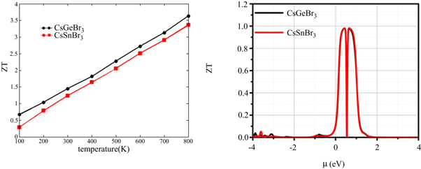
Figure 7. The plots of efficiency verses chemical potential for CsGeBr3 and CsSnBr3 calculated by using BoltzTrap code.
Download figure:
Standard image High-resolution image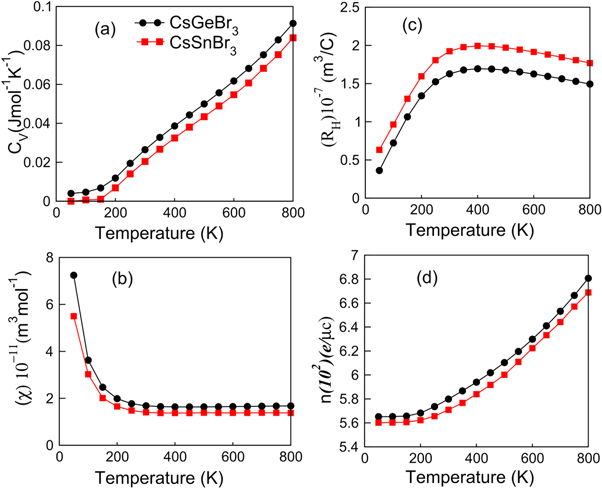
Figure 8. The plots of (a) specific heat capacity, (b) magnetic susceptibility, (c) Hall coefficient and (d) number electron density CsGeBr3 and CsSnBr3 calculated by BoltzTrap Code.
Download figure:
Standard image High-resolution image
The thermodynamic characteristics are further illustrated by computing the specific heat capacity (Cv), susceptibility (χ), Hall coefficient (RH) and electron density (n), which are plotted against temperature in figures 8(a)–(d). The specific heat capacity Cv is explored to understand the device capability for withstanding the external temperatures. As heat transfer is mediated through the lattice (phonons) and free carriers. As the classical way (i.e., Dulong-Petit law) of treating atomic vibrations as having independent frequency is limited to explain the low temperature behavior of Cv, therefore, consideration of the coupled atomic oscillations verifies the experimental data at all temperature [56–59]. Both perovskites exhibit increasing specific heat capacity with the temperature up to 800 K as apparent in figure 8(a), which reveal their high potential to withstand to the external temperatures. Moreover, comparatively higher thermal stability is computed for CGB because the slope of its Cv curve is greater than that of CSB. The magnetic susceptibility (χ) illustrates the way perovskites respond to the applied magnetic field. The computed χ for both CGB and CSB, as presented in figure 8(b), shows a sharp decrease up to 200 K and nearly a constant value 2 × 10–11 m3 mol−1 is exhibited between 200–800 K. The decreased χ at higher temperature evidences the suppressed role of magnetic response at higher temperatures, which becomes an important aspect to know before practical utilities of both perovskites.
The Hall co-efficient (RH) is revealed from the induced electric field by dividing it with the product of carrier density and strength of the employed magnetic field and used to investigate the resistance of a material under Hall geometry. The computed RH for both perovskites, as plotted in figure 8(c), increases with temperature up to 400 K and exhibits a slight decrease between 400–800 K. The increasing RH with the temperature might be due to the enhancing phonon contributions, due to which, scattering increasing causing higher resistive effects. The slight decay in RH at high temperatures might be justified with the fact that more charge carriers are thermally liberated in the studied perovskites, and resultantly, the carrier mobility improves. Typical semiconductors are characterized as having directly linked carrier and Hall mobilities [60]. Moreover, the positive sign of computed RH elucidate the dominant role of holes for the carrier conduction, which is also found consistent with the p-type nature observed in the computed band structures, shown in figure 2. Furthermore, the increasing RH up to 400 K illustrate increasing carriers conductivity, which is consistent with increasing electrical conductivity, as shown in figure 5(a), and hence, good agreement between the computed parameters is evident. The carrier density increases with temperature for both CGB and CSB as shown in figure 8(d), which shows that increasing thermal energy liberates more free carriers. In summary, the predicted high thermoelectric efficiency and good thermal stability suggests both perovskites as suitable novel materials for a variety of thermal applications.
4. Conclusions
The systematic DFT based study of mechanical, thermoelectric and optical properties of Cesium based bromides has been done for evaluating the energy renewable device applications. The thermodynamic, mechanical and structural stabilities of both perovskites are elucidated through the negative enthalpy of formation, Born stability criteria and Goldschmidt's tolerance factor. A ductile behavior has been found for both perovskites. Both perovskites are found optically active in the visible region, due to high absorption and low reflection as well as the optical loss factor. The accuracy of the optical parameters is found due the verification of Penn's model. The computed thermal efficiency has been found very high for these perovskites exhibiting high thermal stability that suggest both as significant potential candidates for thermoelectric applications. The stable cubic phase of both perovskites, showing maximum energy absorption forthe visible energies and best thermoelectric efficiency indicate that both perovskites are appropriate for novel energy renewable device applications.
Acknowledgments
This research project was supported by a grant from the 'Research Centre of Female Scientific and Medical Colleges', Deanship of Scientific Research, King Saud University.