

Abstract
CdS:Dy films were prepared by CSVS method on the cleaned glass substrates. The influence of Dy doping on the optical properties of CdS thin (500 nm) films was studied. The presence of narrow lines of bound and free excitons in the photoluminescence, reflection and absorption spectra shows a remarkable optical quality of the investigated films. The temperature dependence of the band gap of the films was studied on the basis of measurements of the energy position of the free excitons. A decrease in the anisotropic crystal field and the effect of depolarization of free exciton absorption spectra with increasing temperature are observed. It was concluded that the efficiency of CdS:Dy thin films photovoltaic applications can be further increased.
Export citation and abstract BibTeX RIS
1. Introduction
It is well-known that the band gap is one of the most important characteristics of semiconductor materials. Usually, the determination of the band gap is performed by the way of approximation of the absorption edge using the Tauc relation (for direct allowed band-to-band transitions this relation is the following: (αhν)1/2 = A(hν − Eg), where hν is the energy of light, Eg is the band gap, A is the slope of the Tauc plot in the linear region). The band gap is determined by plotting the (αhν)1/2 versus (hν) [1–4]. The extrapolation of the fitting line to its intersection with the energy axis gives the value of the band gap. This method is very widely used to characterize various semiconductor thin films [5–8].
It should be noted that for semiconductor materials, especially, polycrystalline thin films the light transmission depends not only on its absorption due to the transitions between the valence and conduction bands. The formation of absorption edge is also due to additional absorption caused by the presence of different types of intrinsic or impurity defects, lattice strain etc [5–8]. This absorption is associated with the optical transitions between the defect levels and one of the energy bands, and not caused by band-to-band transitions. Besides, the processes of exciton (electron)-phonon interaction also affect the shape of the absorption edge, which covers a wide region of absorption coefficients (several orders of magnitude). So, the absorption edge of semiconductor materials can in fact be represented by a superposition of the absorption of different nature.
Thus, the Tauc method is based on the approximation of the absorption edge, the shape of which strongly depends on the presence of different types of defects in the films. Therefore, the point of the intersection with the energy axis always shifts to the low energy region relative to the energy of the maximum of free exciton (FE) lines. It is well known that the band gap of the semiconductor films corresponds to the energy of FE plus the binding energy of the exciton. It should be noted that the shift of the point of the intersection depends on the optical quality of the films. This means that the obtained value of the band gap is always reduced compared with its real value. At the same time, there is a very exact method for determining the band gap of thin films based on optical measurements of exciton spectra. Here, we demonstrate this method using CdS:Dy thin film as an example.
The interest in the study of CdS thin films is due to the fact that at present they are widely used as window layers in the top of tandem high efficiency solar cells based on CdS–CdTe and CdS–Cu(In, Ga)Se2 [9–11]. One of the effective methods for improving their physical properties is doping with impurity atoms. It should be noted that the rare earth elements play an important role among impurity atoms since they allow improving the electronic properties and optical quality of semiconductors [12, 13]. They may be considered as effective gettering agent for residual impurities in semiconductor materials [14, 15].
The aim of this work is to study the optical properties of Dy-doped CdS thin films, as well as to exactly determine their band gap and study its temperature dependence on the basis of measurements of the reflection and absorption spectra of excitons.
2. Experimental details
CdS:Dy thin films were deposited by close-spaced vacuum sublimation (CSVS) method on the cleaned glass substrates under the evaporator temperature Te = 1173 K, the substrate temperature Ts = 573 K, and the growth time was 4 min. The stoichiometric powder of CdS doped with Dy as the initial material was used. CSVS technique is described in detail in [16]. XRD studies were carried out with a DRON 4-07 diffractometer using KαCo radiation source. Structural parameters, namely, the average grain size in the layers, coherent scattering domain (CSD) size and microdeformation level (ε) were estimated using the methods described in [16]. The thickness measurements of the investigated thin films were carried out with a stylus profiler 'Dektak 150', using the following measurement parameters: scan length of 400 μm, scan resolution of 0.053 μm/sample, stylus force of 10 mg. The optical measurements were performed using an SDL-1 grating spectrometer. The photoluminescence (PL) spectra were excited by an LED with λ = 395 nm and power of 100 mW. The reflection and absorption spectra were measured using an incandescent lamp with a continuous spectral region. The spectral resolution of the system was of the order of (0.1–0.2) meV.
3. Results and discussion
The results of x-ray diffraction measurements of the investigated CdS:Dy films deposited at Te = 1173 K and Ts = 573 K are presented in figure 1. The observed diffraction peaks at 30.92°, 32.92°, 42.84°, 56.24°, 61.08°, 64.34°, 72.02° and 90.58° are associated with the (002), (101), (102), (103), (112), (004), (104), (105) planes of the wurtzite phase. The peaks caused by other phases were not observed. The most intense peak corresponds to the (002) plane. So, this indicates that the optical c-axis is perpendicular to this plane, which coincides with the substrate surface. Thus, doping CdS films with Dy let us deposit such films with a clearly expressed texture and a stable wurtzite phase. The value ε for CdS:Dy films was determined from the studies of the physical broadening of (002) diffraction peak [13]. The obtained results indicate that these value in the [002] direction, parallel to the c-axis, is smaller than in the [103] direction, inclined to this axis. The microstress level for CdS:Dy films corresponds to the value ε(002) = 0.62 × 10⁻³, which indicates a high crystal quality of the investigated thin films. The CSD size for the [002] direction equals 62.2 nm [13]. Previously it was shown that the investigated CdS:Dy films have a highly dispersed structure with the grain size (d) from smaller than 0.1 μm to 1.0 μm [13]. The layer thickness of the films was equal to 0.5 μm.
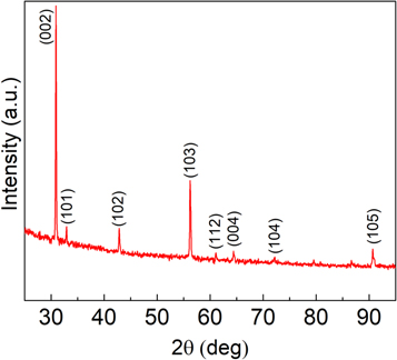
Figure 1. X-ray pattern of CdS:Dy films deposited at the evaporator temperature Te = 1173 K and the substrate temperature Ts = 573 K.
Download figure:
Standard image High-resolution imageEarlier it was shown that PL spectra of CdS:Dy films contain emission of donor-acceptor pairs, free and bound excitons [13]. In figure 2 the PL spectrum in the spectral region of the fundamental absorption is presented. Here the emission of sharp lines is observed at 2.5484 eV and 2.5364 eV, which are associated with the donor and acceptor bound excitons, namely D°X- and A°X-lines, respectively [17]. FE are also observed in reflection spectra (curve 2). The appearance of A and B peaks is caused by trigonal crystal field splitting of the valence band [18].
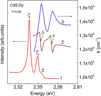
Figure 2. Exciton PL, reflection and absorption spectra of CdS:Dy thin films at T = 4.5 K (curves 1–3, respectively).
Download figure:
Standard image High-resolution imageSince the intensities of the A and B lines of excitons are almost equal, this indicates that the optical axes of crystalline grains of CdS:Dy films are preferably oriented perpendicular to the substrate surface. This result is also supported by the structural measurements of CdS:Dy thin films. The energy positions of A and B excitons, which are determined by the position of the middle point between the minimum and the maximum of the reflection dispersion curve, also make it possible to determine the crystal field splitting (ΔEcr) for CdS:Dy films. This value corresponds to the energy of 17 meV at T = 4.5 K. The observation of FE in the reflection spectrum, as well as free and bound excitons in the PL spectrum for the investigated CdS:Dy films indicates the excellent optical quality of these films. A high optical quality of the films also makes it possible to observe FE in the absorption spectra, which is shown in figure 2 (curve 3). The energy positions of the A and B exciton bands in the exciton reflection and absorption spectra coincide.
As was noted above, the band gap of the investigated CdS:Dy film corresponds to the energy of A FE (2.5536 eV) plus the binding energy of exciton (0.028 eV), i.e. 2.5816 eV, which practically coincides with the band gap for bulk single CdS crystals at 4.5 K (2.5826 eV) [19, 20].
The exciton reflection and absorption spectra obtained in the temperature region from 4.5 to 210 K are represented in figure 3. It can be seen that the increase in temperature causes a long-wavelength shift of the exciton A and B bands and their broadening.

Figure 3. (A) The temperature dependence of exciton reflection spectra (curves 1–6 correspond to 4.5, 10.0, 20.0, 40.0, 60.0 and 70 K, respectively) and (B) exciton absorption spectra (curves 1–7 correspond to 25.0, 70.0, 100.0, 130.0, 160.0, 180.0 and 210.0 K, respectively) for CdS:Dy films where the ordinate axis corresponds to curve 1. Curves 2–6 are slightly shifted vertically.
Download figure:
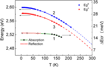
Standard image High-resolution imageAs can be seen from figure 4 (curve 1), the value ΔEcr is practically constant in the temperature region below 130 K and then it decreases with increasing temperature to 170 K. In our opinion, such temperature dependence may be caused by the deformation of CdS:Dy thin films as a result of different thermal expansion of the films and the glass substrate. As can be seen from figure 4, at the low temperatures (<130 K), the value ΔEcr is maximal and does not depend on temperature. We assumed that the crystallographic orientation of the crystalline grains with the optical c-axis perpendicular to the substrate surface is also maximal in this temperature region. At higher temperatures, the depolarization of the exciton absorption spectra occurs as a result of a certain decrease in the orientation of the c-axis perpendicular to the substrate surface.
Figure 4. The temperature dependence of the value ΔEcr (curve1) and the band gaps (curves 2 and 3) for CdS:Dy films. Curves 2 and 3 were obtained by fitting using the equation (1), and correspond to  and
and  band gaps, respectively.
Download figure:
Standard image High-resolution image
Figure 3 also shows the temperature dependence of the energy position of the band gaps (curves 2–3). The results obtained are well fitted numerically by the following formula [21]:

where α and β are the fitting parameters.
The values α and β are taken to be 1.4 × 10⁻³ eV K−1 and 862.2, as well as 1.7 × 10⁻³ eV K−1 and 1171, for  and
and  respectively. It should be noted that the value EgA(0) = 2.5824 eV exactly coincides with the values 2.5825 and 2.5826 eV, obtained for the bulk CdS crystal, from the results of measurements of their exciton PL and reflection spectra, respectively [18, 22]. At the same time, the values EgA(300) and EgB(300) correspond to 2.4763 and 2.4911 eV, respectively.
In summary, one of the unique and novel results of our work is the observation of the FE lines in the reflection and absorption spectra of CdS thin films, which appear due to the doping with Dy and also due to optimization of the technological conditions of the films deposition. It was shown that the obtained films have excellent crystalline and optical quality both at the surface (exciton reflection spectra) and in their volume (exciton absorption spectra). In our opinion, the decisive factor in fabrication of such films is the manifestation of the 'cleaning' effect of residual impurities as a result doping of CdS films with Dy. The optical transmittance of CdS:Dy thin films in the range of transparency (600–800 nm) at room temperature has reached about 80%.
Here, we proposed an effective and very exact method for determining the band gap of semiconductor thin films based on the results of the exciton spectra measurements which can be used for any semiconductor thin films. The measurements of the above mentioned exciton spectra at different temperatures let us determine the temperature dependence of the band gaps for the optical transitions between two upper valence bands and the conduction band. It was found that the band gap of thin CdS:Dy films matches exactly to the band gap of CdS bulk crystals. Thus, the data, presented in the work, can be considered as novel exciting results regarding the correct determination of the band gap of semiconductor thin films. This is also convincing evidence that the different band gap values obtained for the semiconductor thin films deposited under different technological conditions do not correspond to real band gaps, but are due to their different crystalline and optical quality.
In our opinion, the value of the energy obtained by the Tauc method only enables preliminary estimation of the optical band gap and obtaining important information regarding the dependence of the optical quality of thin films on the technological conditions of their deposition.
In this work for the first time the decrease in the splitting of the valence band by an anisotropic crystalline field was detected. It was shown that this may be due to the heterogeneous deformation of CdS:Dy thin films in the depth from their surface at low temperatures.
As mentioned above, the investigated CdS thin films relate to very important semiconductor materials, since they are widely used as window layers in the top of the tandem high efficiency solar cells. Therefore, our findings, presented in the work, also show a great possibility for better use of these films. In particular, they make it possible to improve considerably the optical properties of CdS films by Dy doping, which can be very useful for further increasing the efficiency of their photovoltaic applications.
Acknowledgments
This research has been supported by the National Academy of Sciences of Ukraine (Grants Nos. BС-188-15) and the Ministry of Education and Science of Ukraine (Grant Nos. 0116U002619).