

Abstract
Sol-gel synthesized bismuth ferrite (BiFeO3) nanoparticles (NPs) were encapsulated with SiO2 by the Stöber method. The structural and microstructural studies were carried out by x-ray diffraction (XRD), Fourier transform infrared spectroscopy (FTIR), high resolution transmission electron microscopy (HRTEM) and field emission scanning electron microscopy (FESEM). The XRD pattern revealed the coating of SiO2 on distorted rhombohedral (R3c) structured BiFeO3 (BFO). The particle size of BFO was estimated to be 100–120 nm. The inter-planar spacing between the (1 1 0) planes was found to be 0.28 nm. The coating of amorphous SiO2 shell on crystalline BFO was quite evident from the TEM micrographs. The presence of O–Si–O stretching vibration in FTIR spectra reconfirmed the coating of SiO2. The direct bandgap energy was calculated to be 2.02 eV for BFO and 2.12 eV for BFO@SiO2 (from UV–vis spectra). The optical absorption was observed to be higher for BFO@SiO2 than BFO. These NPs may be used as photoelectrodes in dye sensitized solar cell application.
Export citation and abstract BibTeX RIS
1. Introduction
Since its inception in 1980, core/shell nanostructures have been attracting researchers in many areas of science & engineering, medicine, biotechnology etc. Basically, the core/shell structure is formed with the combination of two or more materials, where one acts as a core and the other covers the core, i.e. the shell. There are many possible types of core/shell nanostructures based on different core shapes like nanotubes, nanowires etc. and different types of shells like bi-layered, composite or multi-layered shell. These nanostructures are characterized with the properties of both the core and shell. The properties of the core are protected by the shell. In some cases, the coupling between the core and shell results in; magnetoelectric (ME) effect, heterojunction for energy storage, quantum confinement effect and surface plasmon resonance etc [1–3].
Coating silica on ceramics/magnetic nanoparticles is a promising and important approach for both scientific studies as well as technological applications. Amorphous silica is a good choice as a shell material because it prohibits agglomeration and hence well dispersion in liquid medium or polymer matrix. It also prevents erosion in acidic medium and maintains thermal and chemical stability. There are quite a few reports on silica shell over various core materials such as α-Fe2O3 [4], CoFe2O4 [5], CoZnFe2O4 [6], Fe3O4 [7, 8] and BiFeO3 (BFO) [9–11]. The silica shell on BFO core particles has shown significant enhancement in dielectric and magnetic properties. Moreover, metal oxides (semiconductor)-SiO2 composite has been used for making phoeletcrodes in dye-sensitized solar cells (DSSCs), where the SiO2 shell plays a role in minimizing interfacial recombination at the semiconductor/electrolyte interface [12]. However, the optical properties of BFO@SiO2 particles are hardly addressed, which may claim its candidature as photoelectrodes in dye-sensitized solar cells (DSSCs).
The co-existence of ferroic properties at room temperature attracts the attention of researchers for studying BFO from theoretical and practical standpoint. It has been considered as a suitable candidate for applications in multifunctional devices. Bismuth ferrite is a rhombohedrally distorted perovskite material with space group R3c, which exhibits multiferroic property near room temperature [13]. It is an environment friendly lead-free material with interesting multiferroic and optical properties. It's applications are still limited due to presence of secondary phases during the synthesis, weak magnetic characteristics, low ME coupling and high leakage current [10, 14]. These drawbacks can be overcome by careful preparation and post synthesis processes such as doping and coating of BFO with other materials respectively. Among these, coating of BFO with other materials could be an interesting way to form a heterostructure at interface which may give exciting results in optical, electrical and magnetic applications.
In this study, we report the synthesis and characterization of BFO@SiO2 core/shell NPs. To tune their functionality for wide range of applications, SiO2 has been chosen as the shell material on BFO core nanoparticles. Attempts have been made to investigate the structure, microstructure, and optical properties through analytical techniques.
2. Experimental details
2.1. Synthesis of BFO using sol-gel method
Bismuth ferrite nanoparticles were synthesized using sol-gel combustion method. Analytical grade (purity, 99.99 %) Bi(NO3)3·6H2O and Fe(NO3)·9H2O were used as precursors. First, bismuth nitrate was dissolved in 1 N nitric acid at 60 °C and iron nitrate was added to the solution and then constantly stirred at 60 °C to obtain a sol. Citric acid was added to it in 2:1 molar ratio and stirred vigorously at 60 °C for 2 h. The light brownish solution was kept on the hot plate at 60 °C (without stirring) for several hours to obtain a thick gel. The gel was transferred to a hot air oven maintained at temperature 220 °C. After a few hours, the gel was observed to be completely dried and auto ignited releasing large amount of gases. The dark brownish powder was collected and subsequently ground and calcined at 500 °C in air for 3 h.
2.2. Preparation of BFO@SiO2 nanoparticles
The BFO nanoparticles (NPs) were coated with SiO2 by the Stöber method [15]. First, 1.5 g of BFO NPs was dispersed in 700 ml of ethanol by sonication. The mixture was kept on the magnetic stirrer and 10 ml of NH3 solution (25 wt%) was then added drop wise. This was followed by the addition of tetraethyl orthosilicate (Si(C2H5O)4) with concentration of 2% at constant stirring for 24 h. The SiO2 coated BFO particles were allowed to sediment due to gravity and the excess silica as supernatant. The excess silica was removed and the coated BFO was washed with DI water and ethanol for four times. The BFO@SiO2 NPs were dried in the oven at 200 °C for 2 h.
2.3. Characterization
The crystal structure of BFO and BFO@SiO2 samples were characterized by using x-ray diffractometer (XRD) (PANalyticalX'pert PRO) with Cu Kα radiations. The morphology of the samples was observed using a high resolution transmission electron microscopy (HRTEM) (FEI-FP-5022/22Tecnai G2 20 S-TWIN) and a field emission scanning electron microscopy (FESEM) (Nova Nano SEM-450). An FTIR spectrometer (JASCO-FT/IR 4100) was used for studying the vibrational properties. The optical properties were studied from the absorption spectrum of a UV–vis spectrophotometer (SCHIMAZE-2450).
3. Results and discussion
3.1. XRD
Figure 1(a) shows the XRD pattern of the BFO NPs. The diffraction peaks are observed to be sharp and demonstrate a highly rhombohedral oriented crystal structure according to the JCPDS file no. 86-1518. An impurity phase of Bi25FeO40 is also found with a very small intensity. In the angle range of 31–32°, a partial overlap of doubly split peaks (1 0 4) and (1 1 1) of BFO is observed. This shows the coexistence of small percentage of orthorhombic phase with the parent rhombohedral phase [16]. In figure 1(b), the XRD pattern of BFO@SiO2 NPs exhibits a combination of both BFO and SiO2 phases. The intensity of peaks for BFO phase decreases after SiO2 coating. Moreover, a broad peak centered at 23° is observed. This confirms the coating of amorphous SiO2 on the surface of BFO NPs.

Figure 1. The XRD patterns of (a) BFO NPs indexed accordingly to space group R3c (*some traces of Bi25FeO4), and (b) BFO@SiO2 NPs.
Download figure:
Standard image High-resolution image3.2. Morphology of NPs
3.2.1. SEM study
Figure 2(a) displays typical FESEM image of BFO NPs. The image of BFO exhibits agglomerated NPs with a size distribution of 70–150 nm. The average particle size has been determined to be 100 nm with image J software (shown in figure 2(b)). The morphology of SiO2 coated BFO particles are shown in figure 2(c). As shown in figure 2(d), the particle size is observed in the range of 90–190 nm after SiO2 coating (with an average size of 113 nm). The increase in the particle size confirms SiO2 shell formation.
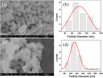
Figure 2. (a) FESEM image of BFO NPs and (b) their size distribution, (c) FESEM image of BFO@SiO2 NPs and (d) their size distribution.
Download figure:
Standard image High-resolution image3.2.2. TEM study
In order to obtain detail information on as-prepared core/shell BFO@SiO2 NPs, bright field HRTEM micrographs were recorded. Figure 3(a) shows the typical morphology of the BFO particles. The particles are formed as hexagonal and cubic shapes. This could be due to the calcination temperature, that results in fraction of particles to be cubic i.e. the orthorhombic phase (mentioned in XRD analysis). The size of the particles is estimated from the TEM image. It has been found to be 100–120 nm, which is close to the value obtained from FESEM. Figure 3(b) shows a typical polycrystalline structure without any amorphous region at particle surface. The inter-planar spacing is calculated to be about 0.28 nm which is shown in inset to figure 3(b). As the (1 1 0) surface has the lowest surface energy, the structure prefers to grow along [1 1 0] direction [17].
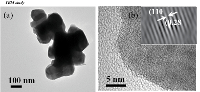
Figure 3. (a) TEM and (b) HRTEM images of BFO NPs and the inset in (b) shows the interplanar spacing for plane (1 1 0).
Download figure:
Standard image High-resolution imageFigure 4(a) displays the TEM image of BFO@SiO2 NPs. The TEM image reveals the formation of well crystalline BFO NPs with the amorphous SiO2 being deposited on the particles. The particles have amorphous shell and crystalline core structure as confirmed by HRTEM image (figure 4(b)). The inter-planar distance measured from the adjacent lattice fringes has been found to be about 0.28 nm. This indicates that the crystallinity of BFO cores persists after SiO2 coating.

Figure 4. (a) TEM and (b) HRTEM images of BFO@SiO2 core/shell NPs.
Download figure:
Standard image High-resolution image3.3. FTIR spectroscopy
FTIR spectroscopy is used to reveal the functional groups of BFO and BFO@SiO2 NPs. Figure 5 displays the spectra of samples with indication (arrow mark) of the presence of functional groups at a particular wave number. The metal oxide bands in the range of 400–600 cm−1 usually attribute to the Fe–O stretching and bending vibrations in octahedral FeO6 unit, which confirm the formation of perovskite structure in the samples [18]. The absorption peaks at 444 [19] and 552 cm−1 [20] correspond to the bending vibration and the Fe–O stretching modes in the FeO6 octahedral site respectively. The coating of SiO2 NPs can be confirmed from the observed O–Si–O bands at 474 cm−1 and 1111 cm−1 [21]. This suggests a strong interaction between the BFO core and SiO2 shell at the interface.

Figure 5. FTIR spectra of BFO and BFO@SiO2 NPs.
Download figure:
Standard image High-resolution image3.4. UV characterization
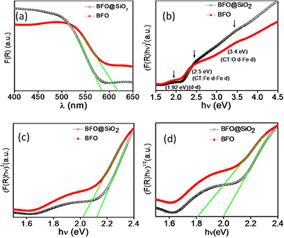
To investigate the optical properties of BFO and BFO@SiO2 NPs, the UV–vis diffused reflectance spectra were recorded at room temperature. The diffused reflectance of the NPs was measured with a UV–vis spectrometer with an integrating sphere attached (ISR 2200). The measurement was performed in the wavelength range of 200–900 nm using barium sulphate as a reference. The Kubelka–Munk function, F(R), also known as optical absorption, was calculated from the diffused reflectance (R) of the NPs by the relation F(R) = (1 − R2)/(2R). Absorption spectra of the BFO and BFO@SiO2 are shown in figure 6(a). The UV–vis spectra demonstrate that the BFO@SiO2 NPs can absorb significantly more light in the 400–510 nm region than BFO, but the optical absorption in the wavelength region of 510–650 nm exhibits lower value than BFO.
Figure 6. Plots of (a) optical absorption F(R) versus λ, (b) (F(R)hν)2 versus hν, in the energy range 1.5–4.5 eV, (c) (F(R)hν)2 versus hν, and (d) (F(R)hν)1/2 versus hν, in the range of 1.5–2.4 eV of BFO and BFO@SiO2 NPs.
Download figure:
Standard image High-resolution image
Figure 6(b) displays the curve between (F(R)hν)2 and (hν) in the energy range of 1.5–4.5 eV. A shoulder centered at 1.92 eV is observed, which can be assigned an Fe3+ crystal field excitation (6A1g → 4T2g) [22, 23]. These excitations are forbidden formally because they change the total spin from S = 5/2 to S = 3/2 of Fe3+ ion. However, spin orbit coupling relaxes the spin selection rule and gives rise to these transitions [24, 25]. Thereafter, the absorption increases significantly above 2 eV, with small shoulders centered at 2.5 eV and near 3.4 eV. The transition band centered at ~2.5 eV may be assigned to the Fe13d–Fe23d intersite electron transfer, whereas the other band around ~3.4 eV, may be associated with the interatomic O2p-Fe3d transition. A noticeable shift in these transition bands clearly indicates the changes in FeO6 local environment in case of BFO@SiO2 NPs. Due to some limitations of the UV–vis spectrometer used in this work, the absorption below 200 nm could not be recorded. This prohibited us to estimate the energy band gap of SiO2 (>5 eV).
To analyse the effect of associated transitions, the energy band gap of BFO and BFO@SiO2 NPs has been determined from the spectra using Tauc's law:

where α = F(R), hν is the photon energy, A is a constant, Eg is the optical energy band gap. The exponent n represents the type of optical transitions between valence and conduction bands. In case of direct allowed band transition, n = 1/2, while indirect allowed transition is expected for n = 2 [26]. Figures 6(c) and (d) display the plots between (F(R)hν)2 − (hν) for the direct allowed transition and (F(R)hν)1/2 − (hν) for indirect allowed transition, in the energy range of 1.5–2.4 eV.
The band gap is determined from an intercept on X-axis, made by extrapolating a straight line. The value of the band gap is found to be 2.0 eV (figure 6(c)), which is consistent with those reported for BFO nanostructures (1.8–2.5 eV) [27, 28]. The band gap for the sample BFO@SiO2 is 2.1 eV. Considering indirect transitions (figure 6(d)), the Eg values are somewhat lower as compared to the corresponding Eg values, obtained from direct transitions. The values obtained for Eg are presented in table 1. The table also shows the values of Eg obtained from the absorption edge (using Eg = 1240/λ) of figure 6(a). As per the direct transitions, the values obtained for Eg are nearly matching with that of calculated values using the above relation.
Table 1. Experimental Eg values of BFO and BFO@SiO2 NPs obtained from various plots.
| Sl. no. | Sample | Band gap energies (Eg in eV) | ||
|---|---|---|---|---|
| F(R) versus λ (figure 6(a)) | (F(R)hν)2 versus hν (figure 6(c)) | (F(R)hν)1/2 versus hν (figure 6(d)) | ||
| 1 | BFO | 2.01 | 2.02 | 1.81 |
| 2 | BFO@SiO2 | 2.13 | 2.12 | 2.01 |
In literature, we find a lot of contradicting arguments in predicting BFO as direct/indirect band gap semiconductor from optical absorption data. To name a few, Lin et al [29] reported the direct band gap of BFO thin films to be 2.3 eV. Based on the lack of the characteristic shape of the (αhν)1/2 versus hν plot, they have ruled out the possibility of indirect band transition. However, Mc Donnnell et al [30] have observed simultaneous presence of direct and indirect transitions for BFO experimentally and computationally.
4. Conclusions
BiFeO3 NPs were prepared using sol-gel combustion technique. The BFO NPs were calcined at 500 °C for 2 h. The core–shell BiFeO3@SiO2 NPs were synthesized by the Stöber method. Their structure and compositions are confirmed by XRD patterns, FESEM, HRTEM micrographs and FTIR spectra. The size of BFO NPs is in the range of 100–120 nm. The size of NPs is increased after SiO2 coating on BFO core. The thickness of SiO2 shell at a specified location is found to be 4 nm. The diffused reflectance spectra are recorded in the wavelength range of 200–900 nm and the optical band gaps are calculated using Tauc's relation for BFO and BFO@SiO2 NPs. The BFO@SiO2 NPs exhibited a marginally higher band gap than BFO. The observed enhancement in optical absorption may find their use as photoelectrodes in DSSCs with better thermal and chemical stability.