

Abstract
We report the synthesis of silicon-vacancy (SiV) incorporated spherical shaped ultrananocrystalline diamond (SiV-UNCD) particulates (size ∼1 μm) with bright luminescence at 738 nm. For this purpose, different granular structured polycrystalline diamond films and particulates were synthesized by using three different kinds of growth plasma conditions on the three types of substrate materials in the microwave plasma enhanced CVD process. The grain size dependent photoluminescence properties of nitrogen vacancy (NV) and SiV color centers have been investigated for different granular structured diamond samples. The luminescence of NV center and the associated phonon sidebands, which are usually observed in microcrystalline diamond and nanocrystalline diamond films, were effectively suppressed in UNCD films and UNCD particulates. Micron sized SiV-UNCD particulates with bright SiV emission has been attained by transfer of SiV-UNCD clusters on soda-lime glass fibers to inverted pyramidal cavities fabricated on Si substrates by the simple crushing of UNCD/soda-lime glass fibers in deionized water and ultrasonication. Such a plasma enhanced CVD process for synthesizing SiV-UNCD particulates with suppressed NV emission is simple and robust to attain the bright SiV-UNCD particulates to employ in practical applications.
Export citation and abstract BibTeX RIS
1. Introduction
The development of solid-state single photon sources is much need for the applications like quantum computation and quantum information processing (QIP) applications [1]. The solid-state single photon sources possess great advantages, such as stable emission at room temperature, long-term sustainability, the narrow emission spectrum, low noise emission, and nano-scalability. Therefore, these characteristics of solid-state single photon sources create a huge interest towards quantum computation and QIP applications [2, 3]. Diamond is a remarkable solid-state single photon emission source, due to the presence of various color centers, which can work as eminent single photon sources, such as nitrogen-vacancy (NV) center [4], silicon-vacancy (SiV) center [5], nickel-based NE8 center [6], nickel–silicon complex [7], and chromium-related center [8]. Among all the color centers of diamond, the NV and SiV centers are prominent in quantum computing, QIP and bio-imaging applications, due to their stable emission at room temperature. Most investigations on NV centers have been reported for nanodiamonds (NDs), single crystalline diamond (SCD) films and SCD nanowires [9–14], whereas the SiV centers are present in the polycrystalline diamond (PCD) films and NDs [15–18].
Even though the NV center is a well-established diamond color center as a single photon emitter and fluorescent source in NDs, NV center has limitations in the practical applications due to wide phonon sidebands (PSBs) at 575–850 nm and long excitation lifetime of 25 ns [5, 14]. In contrast, the SiV center is an excellent single photon source, which overwhelms the limitations of NV center by its advantageous intrinsic properties, such as narrow emission spectrum at 738 nm, small PSBs, short excitation lifetime of 1.2 ns, and emission line width of 0.7–7 nm [5, 15, 19, 20]. Furthermore, SiV centers are photoactive in NDs with the size lower than 2 nm [21, 22]. Recently, the SiV center in NDs has conquered a huge attention in optical biomarker applications due to their photostability, biocompatibility, and non-toxicity [23–25].
SiV center in diamond can be produced by ion implantation method, in situ Si doping in microwave plasma enhanced CVD (MPECVD) diamond growth, and high pressure–high temperature diamond growth process [5, 15, 20, 26–31]. Among all these possible routes for synthesis of the SiV center diamond, microwave plasma CVD based diamond films would be a better choice, as this process contributes to brighter SiV emission [30]. Recently, it has been reported that, microcrystalline diamond (MCD) films exhibit stronger SiV's luminescence than that for nanocrystalline diamond (NCD) films, due to less defective structure; here the diamond films are grown on AlN substrate in CVD process with silane as Si doping source [32]. The size dependent SiV spectral properties have been reported for diamond polycrystals with size of 25–1000 nm and PCD with size of 180 nm exhibits the maximum SiV luminescence, which were produced by shock wave synthesis followed by grinding and separation [33]. CVD diamond has been grown on the end face of fused silica optical fibers for NV center's fluorescence waveguiding and silica was used for high-density nucleation [34]. Therefore, it is interesting to study the growth of SiV-diamond on silicon oxide substrates and to investigate the SiV center's fluorescence of SiV-diamond/silicon oxide substrate. In this study, the diamond has been grown on various forms of silicon oxide substrates using different growth plasma, in order to investigate the spectral properties of SiV-diamond from different granular structured diamond samples. Spherical shaped ultrananocrystalline diamond (UNCD) particulates have been successfully synthesized on soda-lime glass fibers using a simple MPECVD process and show a high brightness of 738 nm luminescence from SiV center. A simple process was developed to collect the SiV-UNCD particulates from soda-lime glass fibers to inverted pyramidal cavities fabricated on Si substrates.
2. Experimental methods
It should be noted that the main purpose of this study is to investigate the feasibility of fabricating the diamond particulates with embedded SiV centers via the simple MPECVD process. Three kinds of oxide substrates, including SiO2-coated Si substrate (SiO2/Si), soda-lime glass substrate and soda-lime glass fibers were utilized for the growth of MCD, NCD, and UNCD films, using CH4/H2, CH4/H2/Ar, and CH4/Ar plasma, respectively. All diamond films were grown by using IPLAS setup (Cyrannus, 2.45 GHz) with the growth parameters listed in table 1. For the SiO2/Si substrates, the SiO2 films with the thickness of 300 nm were grown on Si wafer by the thermal oxidation process at 1100 °C. Prior to the growth of diamond films, the planar SiO2/Si and soda-lime glass (flat glass) substrates were subjected to the seeding process by ultrasonication in a methanol solution containing the mixture of diamond powder (about 4 nm in size) and Ti powder (SIGMA-Aldrich) (365 mesh) for 45 min. In contrast, the soda-lime glass fibers of the length about 2 cm and diameter around 5–6 µm were drenched in a solution containing ND particles, such that the ND particles can adhere to the fibers to serve as nucleation sites. In the diamond growth process, no external heating was applied to the substrate; but the substrates were heated up by the bombardment of the species in the diamond growth plasma. The diamond growth temperature was measured by a thermocouple embedded in the substrate holder and was estimated to be around 580 °C for growing MCD films, 540 °C for growing NCD films and 450 °C for growing UNCD films. The growth time of all diamond films were same i.e. 3 h. The optical emission of the diamond growth plasmas were collected using an optical fiber and analyzed by a spectrometer (OCEAN OPTICS USB4000, USA). Presumably, the Si species were incorporated into the diamond films in two steps, i.e., (i) the ion bombardment and/or H2 etching on SiO2-containing surface of the substrates enabled the Si species mixing with the diamond growth plasma, (ii) the Si species were incorporated into diamond during the CVD growth process.
Table 1. Processing parameters in MPECVD for the growth of diamond crystals on SiO2/Si wafer, soda-lime glass and soda-lime glass fibers.
| Diamond type | Process gas composition | Process pressure (Torr) | Microwave power (W) | Growth time (min) | Substrate temperature (°C) | Observed color centre |
|---|---|---|---|---|---|---|
| MCD | CH4/H2 (1:99) | 30 | 1600 | 120 | 580 | NV and SiV |
| NCD | CH4/H2/Ar (1:50:49) | 70 | 1400 | 60 | 540 | NV and SiV |
| UNCD | CH4/Ar (1:99) | 120 | 1200 | 180 | 450 | SiV |
The surface morphology and microstructure of diamond films were examined using scanning electron microscopy (SEM, JEOL-6500) and transmission electron microscopy (TEM; JEOL 2100F), respectively. The bonding structure of these films was studied using the UV-Raman spectroscopy (λ = 325 nm, Lab Raman HR800, JobinYvon). The color center's characteristics of diamond films with different morphology were investigated by photoluminescence (PL) spectroscopy measurements using micro-PL system with the excitation wavelength of 532 nm. PL mapping (550–800 nm) measurements were performed using a laser power of 100 μW with detector integration time of 1 s for all the samples.
3. Results
3.1. Materials characterization
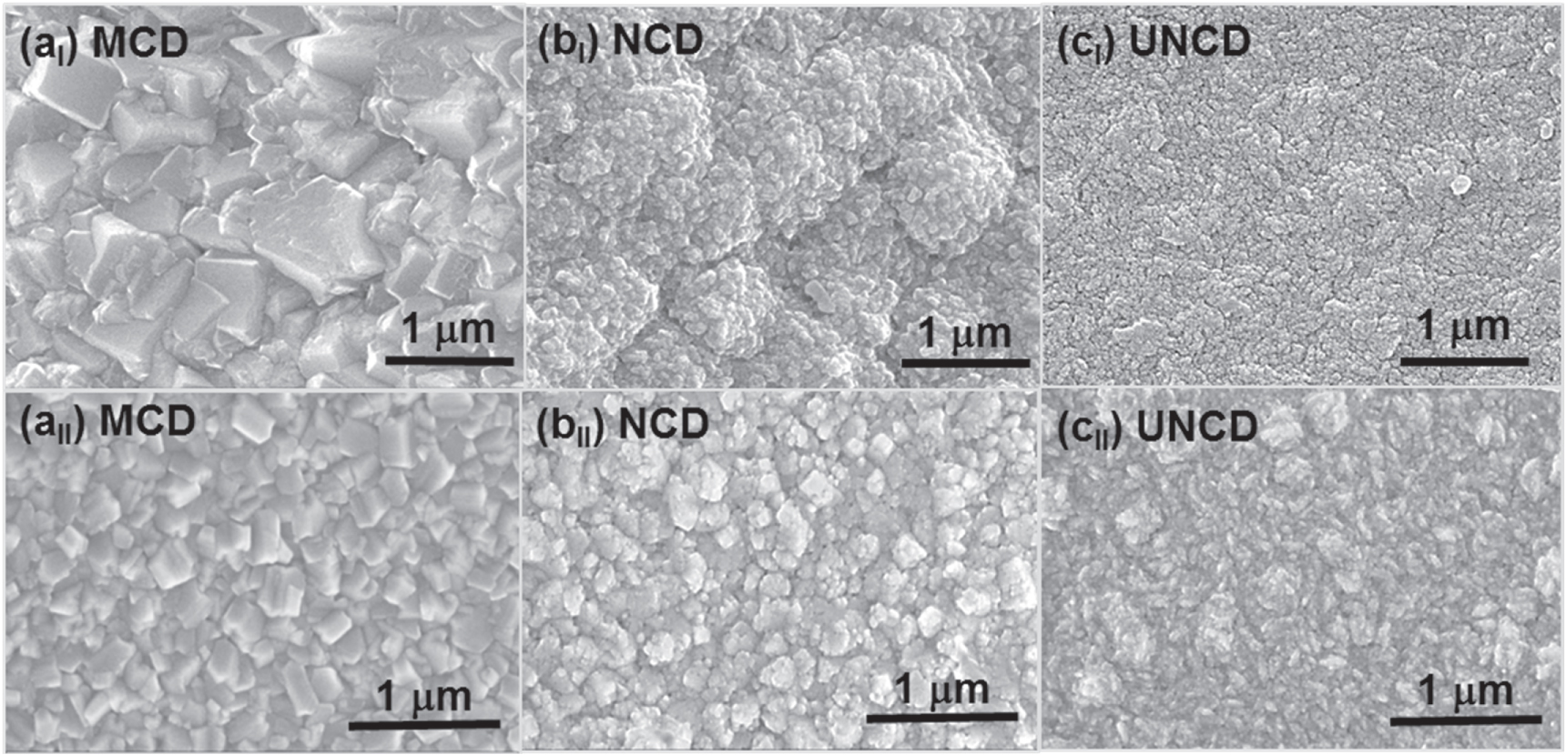
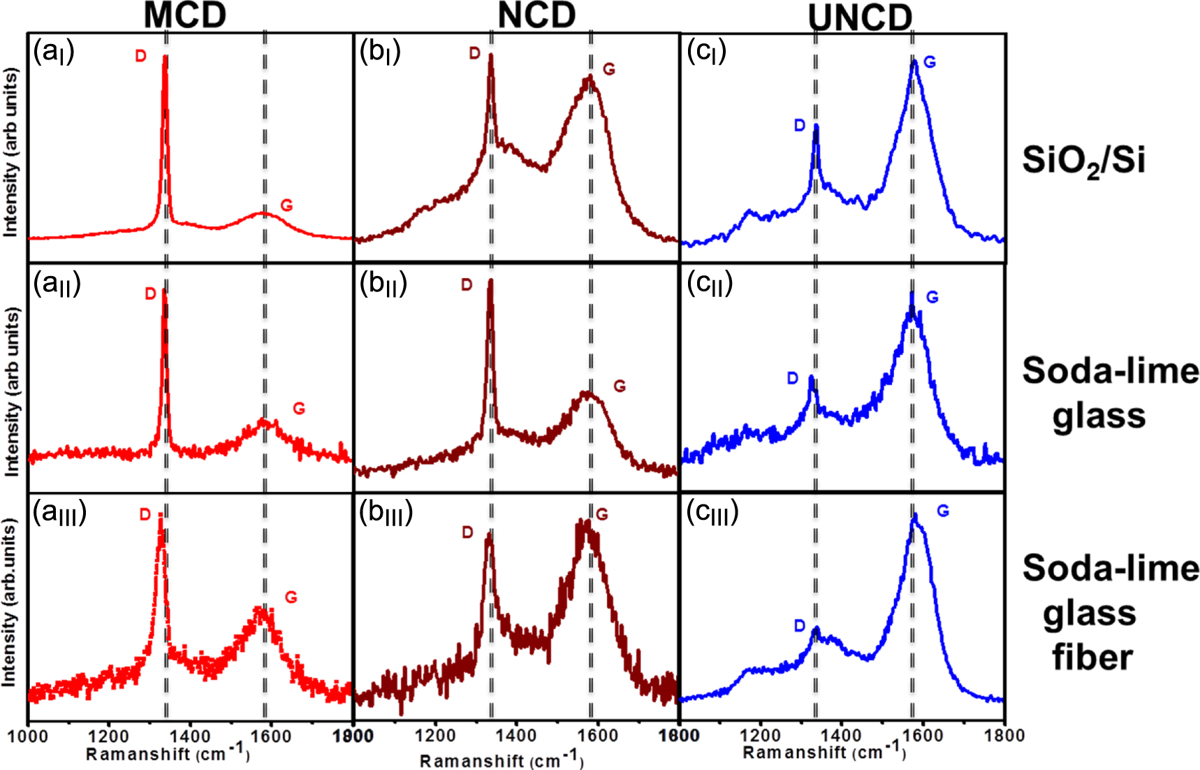
The growth behavior of CVD diamond on planar SiO2/Si and soda-lime glass substrates was investigated first. SEM surface morphologies of MCD films grown on SiO2/Si and soda-lime glass are shown in figures 1(aI) and (aII), respectively, indicating that the MCD films consist of faceted grains with sharp grain boundaries. The grain size is much smaller for the MCD films grown on soda-lime glass, compared with those grown on SiO2/Si, i.e., it is about 1 µm for MCD/SiO2/Si films and is around 300–400 nm for MCD/soda-lime glass films for the same growth time. The UV-Raman spectra of the corresponding films are shown in figures 2(aI) and (aII), respectively, revealing that both MCD/SiO2/Si and MCD/soda-lime glass films depict a sharp Raman peak at 1336 cm−1, corresponding to first-order Raman peak of diamond, and a small broad peak at 1580 cm−1, corresponding to G-band [35, 36]. The calculated ID/IG ratios of the corresponding spectra are showing with values of 0.79 and 0.57, respectively (table 2). The SEM images of NCD films grown on SiO2/Si and soda-lime glass substrates are shown in figures 1(bI) and (bII), respectively. NCD films grown on SiO2/Si substrates show the cauliflower kind of surface morphology, and the ND grains are in the size of 50 nm, which have been agglomerated into big aggregates about 1 μm in size. The NCD/soda-lime glass films seem to form smaller aggregates (∼hundreds of nanometer) compared with NCD/SiO2/Si films. The UV-Raman spectra of the corresponding films are shown in figures 2(bI) and (bII). Both the NCD/SiO2/Si and NCD/soda-lime glass films depict a sharp Raman peak at 1336 cm−1 corresponding to the first-order Raman peak of diamond and a broad peak at 1580 cm−1(G-band) corresponding to the graphitic phase. The G-band in NCD/SiO2/Si (or NCD/soda-lime glass) films is larger in intensity compared with those in MCD/SiO2/Si (or MCD/soda-lime glass) films, which is apparently related to the larger proportion of grain boundary phase presents in NCD films. This could be correlated with ID/IG ratios of the corresponding spectra, (i.e.) the ID/IG = 0.64 for NCD/SiO2/Si and 0.39 for NCD/soda-lime glass (table 2).

Figure 1. SEM micrograph of (aI) MCD, (bI) NCD, and (cI) UNCD films grown on SiO2/Si substrates and those of (aII) MCD, (bII) NCD, and (cII) UNCD films grown on soda-lime glass substrates.
Download figure:
Standard image High-resolution image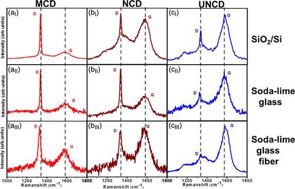
Figure 2. UV Raman spectrum of (a) MCD, (b) NCD and (c) UNCD films grown various kinds of substrates: (aI) MCD, (bI) NCD and (cI) UNCD films grown on SiO2/Si substrates; (aII) MCD, (bII) NCD and (cII) UNCD films grown on soda-lime glass substrates; and (aIII) MCD, (bIII) NCD, (cIII) UNCD films grown on soda-lime glass fibers.
Download figure:
Standard image High-resolution imageTable 2. Raman and PL spectral properties of different granular structured diamond films.
| Sample | ID/IG | ZPL width (nm) |
|---|---|---|
| MCD/SiO2/Si | 0.79 | — |
| MCD/soda-lime glass | 0.57 | — |
| MCD/soda-lime glass fiber | 0.60 | — |
| NCD/SiO2/Si | 0.64 | — |
| NCD/soda-lime glass | 0.39 | — |
| NCD/soda-lime glass fiber | 0.38 | — |
| UNCD/SiO2/Si | 0.44 | 17.3 |
| UNCD/soda-lime glass | 0.81 | 8.8 |
| UNCD/soda-lime glass fiber | 0.60 | 9.4 |
Figures 1 (cI) and (cII) show the SEM surface morphology of UNCD films grown on SiO2/Si and soda-lime glass substrates, respectively. UNCD films grown on SiO2/Si substrates possess a smooth surface with ultrasmall diamond grains, whereas UNCD films grown on soda-lime glass substrates contain aggregates about 50–100 nm in size, which are made up of the ultrasmall grains of size about 5–10 nm. UV-Raman spectrum of UNCD/SiO2/Si films is shown in figure 2(cI), which exhibits a sharp Raman peak at 1333 cm−1 (the first-order Raman peak of diamond), but with smaller intensity compared with those of MCD (or NCD) films. There also exists a broad peak at 1575 cm−1 (the G-band), which is of larger intensity compared with those of the MCD (or NCD) films [35, 36]. Moreover, a small broad peak is observed at 1350 cm−1 (D*-band) representing the disordered carbon and those at 1140 cm−1 (ν1-band) and 1480 cm−1 (ν3-band at), corresponding to transpolyacetylene phase located at the grain boundaries of UNCD films [35, 36]. Figure 2(cII) shows that the characteristics of Raman spectra of UNCD/soda-lime glass films are similar to those of UNCD/SiO2/Si films, but with the much noise signal in the background. Moreover, the ID/IG ratios were calculated to be 0.44 and 0.81 for UNCD/SiO2/Si and UNCD/soda-lime glass, respectively, which indicate the presence of large amount of defects and stress in UNCD/soda-lime glass. The coalescence of ultra-small diamond grains was frequently observed in UNCD films, which induced the formation of large diamond aggregates distributed among the matrix of ultrasmall diamond grains [37].
The diamond films grown on soda-lime glass fibers show markedly different morphology compared to those grown on planar SiO2/Si or soda-lime glass substrates. The MCD/soda-lime glass fibers contain diamond aggregates of island-wise geometry with each of them about micron-size rather than forming a continuous film (figure 3(aI)). Enlarged SEM micrograph shown in figure 3(aII) reveals that the island-wise MCD aggregates actually contain rounded diamond grains of the size of about 300–500 nm. The diamond grains are not faceted as MCD films grown on the SiO2/Si or soda-lime glass substrates. The UV-Raman spectrum shown in figure 2(aIII) reveals the sharp first-order Raman peak of diamond at 1333 cm−1 and a broad Raman peak at 1580 cm−1 (ID/IG = 0.60), which are similar to those of MCD films grown on SiO2/Si or soda-lime glass substrates but with larger background noise. Figure 3(bI) shows the SEM image of highly dense NCD crystals grown on soda-lime glass fibers, whereas figure 3(bII) shows the enlarged SEM micrograph of these NCD crystals. These micrographs reveal that the NCD crystals are spherical in shape with size around 50–70 nm. The NCD crystals are isolated from one another but are spread uniformly all over the fiber. It should be reminded that normally NCD films grown on planar substrates (i.e., SiO2/Si or soda-lime glass substrates) contain columnar structure of size around few tens of nanometers (see figures 1(bI) and (bII)). Here, such a feature has not been observed due to artifacts in soda-lime glass fiber substrate, rather only islands of spherical shape are observed. The UV-Raman spectrum (figure 2(bIII)) of NCD crystals also shows sharp first-order Raman peak at 1332 cm−1 (D-band) and G-band (sp2-bonded carbon) at 1575 cm−1 [35, 36] (ID/IG = 0.38), but with much higher background noise, compared to the NCD grown on planar substrates (SiO2/Si or soda-lime glass).
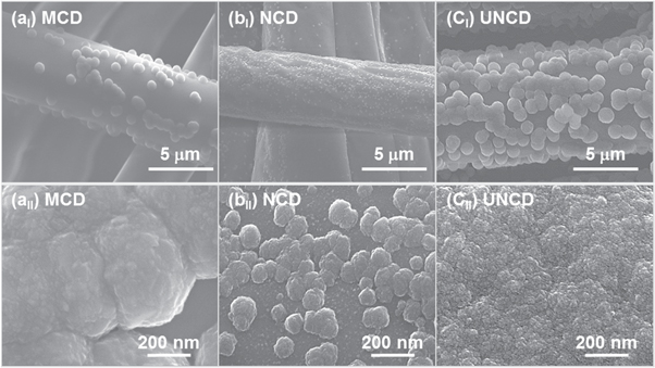
Figure 3. SEM micrograph of (aI) MCD, (bI) NCD, and (cI) UNCD films grown on soda-lime glass fibers. (aII), (bII) and (cII) are the enlarged SEM micrographs of (aI), (bI) and (cI), respectively.
Download figure:
Standard image High-resolution imageFigure 3(cI) shows the low magnification SEM images of UNCD films grown on soda-lime glass fibers, which reveals the presence of spherical aggregates with size around 1 µm. Figure 3(cII) shows the enlarged SEM micrographs, revealing that each UNCD diamond aggregates contain densely populated diamond grains. Although the UNCD/soda-lime glass fibers no longer form continuous films, the microstructure of UNCD films in each diamond aggregates is not much different from those grown on planar substrates (see figure 1(bI)). The UV-Raman spectrum of UNCD/soda-lime glass fibers is shown in figure 2(cIII), which depicts much smaller D-band at 1333 cm−1 from diamond with much larger D*-band at 1350 cm−1 from disorder carbon and G-band at 1577 cm−1 from sp2-bonded carbon [35, 36] (ID/IG = 0.60). This indicates that the proportion of sp2-bonded carbon present in the UNCD films increased markedly relative to the sp3-bonded carbon when the UNCD films were grown on soda-lime glass fibers. The UV-Raman studies show the occurrence of a blue shift in first order Raman peak of diamonds D-band for all samples, which confirms the presence of defects and stress in all diamond films, regardless of morphology. In addition, the UNCD films have shown the evidence of large ensembles disorder carbon.
The microstructure of MCD, NCD, and UNCD films was investigated in more detail using TEM. It should be mentioned that only the diamond films grown on planar substrates (SiO2/Si and soda-lime glass) were examined, as the preparation of the TEM foil for the diamond grown on soda-lime glass fibers is extremely difficult. Figure 4(a) shows the TEM bright field (BF) image of MCD/SiO2/Si film, confirming the large grain characteristics of the MCD films. Inset in figure 4(a) shows the corresponding selected area electron diffraction (SAED) pattern, revealing the presence of discrete diffraction spots corresponding to (111), (220), (311) diamond lattice planes. Moreover, there exist diffraction spots arranged in a continuous ring, suggesting the presence of some randomly oriented small diamond grains coexisting with the large diamond grains. There is essentially no diffuse central ring, indicating very small proportion of sp2-bonded carbon contained in these films. The phase constituents of these films were better demonstrated by the composed dark field (c-DF) images, which is the superposition of several dark field images acquired using different diffraction spots. Figure 4(b) shows the c-DF image of MCD/SiO2/Si film, which confirms the coexistence of large diamond grains with some small diamond grains. The diffraction spots on (111) ring used for composing c-DF images are indicated in inset of figure 4(b). To elaborate the microstructure in detail, high-resolution TEM (HRTEM) images from the region of large diamond grains (region A, figure 4(a)) and the vicinity region of diamond grains (region B, figure 4(a)) were examined. Figure 4(c) illustrates the HRTEM of region 'A' with the corresponding fourier transformed diffractogram, FToc-image, of the whole structure image shown as an inset in figure 4(c). The presence of rel-rods associated with each major diffraction spots in FToc implies that the diamond grains contain a large proportion of planar defects, most probably the stacking fault, which are highlighted in ft1- and ft2-images corresponding to areas 1 and 2, respectively. In contrast, HRTEM images shown in figure 4(d) acquired from the designated region B in figure 4(a), shows the presence of small diamond grains of size around 5–10 nm. Inset in this figure 4(d), the FT0d-image corresponding to the whole structure image in figure 4(d), shows the diffraction pattern arranged in a ring shape, implying the presence of randomly oriented small diamond grains in this region. A diffused ring located at the center of the FT0d image indicates the presence of a-C phase in this region. The existences of small diamond grains and a-C phase in this region are highlighted by the ft3 and ft4 images corresponding to areas 3 and 4, respectively. The presence of small diamond grains together with the large diamond grains in MCD/SiO2/Si films is very much different from the microstructure of MCD films grown directly on Si substrates, in which no small diamond grains was observed. The microstructure of MCD/soda-lime glass films is similar to the one shown in figure 4 (supplementary information, figure S1), inferring that the difference in the microstructure of MCD/SiO2/Si from the conventional MCD/Si films is mainly due to the utilization of oxide substrate materials. The presence of Na species in the substrates seems not markedly altered the granular structure of the MCD films.
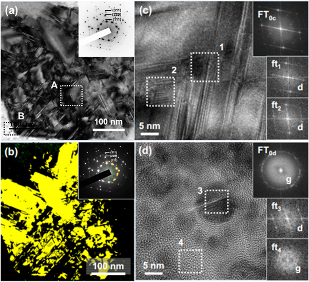
Figure 4. (a) Bright field TEM micrographs of MCD/SiO2/Si films with SAED shown as inset and (b) composed dark field TEM micrographs corresponding to (a); HRTEM image of (c) selected area A and (d) selected area B designated in (a), respectively. The FT0c and FT0d images are fourier-transformed diffractogram corresponding structure images in 'c' and 'd', respectively, whereas the ft1 to ft4 images correspond to areas 1 to 4, respectively.
Download figure:
Standard image High-resolution imageFigures 5(a) and (b) show the BF and c-DF TEM micrograph of NCD/SiO2/Si films respectively, which reveal that the microstructure of these films are similar to that of MCD/SiO2/Si films, except that the grain size of NCD films is much smaller, i.e., they consist of large diamond grains around 100 nm in size, coexisting with the ultra-small diamond grains about 5 nm in size. Inset of figure 5(a) shows the SAED pattern corresponding to (111), (220), (311) diamond lattice planes. Inset in figure 5(b) shows the diffraction spots on (111) ring used for composing c-DF images. TEM structure image in figure 5(c) shows that the large diamond grains (region A, figure 5(a)) also contain planar defects, the stacking faults, which are evidenced by the existence of parallel fringes in figure 5(c) and the presence of the rel-rods in FT0c image (inset, figure 5(c)). The presence of planar defects is further highlighted by the ft1 and ft2 images corresponding to areas 1 and 2 in figure 5(c). Again, TEM structure image in figure 5(d) shows that the ultrasmall grain region (region B, figure 5(a)) contains some sp2-bonded carbon, which is inferred from the central diffuse ring in FT0d image in inset of figure 5(d). The existence of diamond and a-C phase in these materials is highlighted by ft3 and ft4 images, corresponding to areas 3 and 4, respectively, in figure 5(d). The microstructure of NCD films grown on soda-lime glass substrates (supplementary information, figure S2), is similar with those grown on SiO2/Si substrates. The presence of Na-species in soda-lime glass seems not to markedly alter the granular structure of NCD films. Compared with the microstructure of MCD, the grain size of NCD films is about one order of magnitude smaller. The other features, such as the presence of stacking faults in the region of large diamond grains and the presence of a-C phase in ultrasmall grain regions, are essentially the same for both MCD and NCD films. It should be noted that the NCD/SiO2/Si films contain more abundant ultra-small diamond grains, compared with NCD films grown on conventional Si substrates, inferring that the presence of a SiO2 surface in the substrates hindered markedly the nucleation and growth behavior of these diamond films.
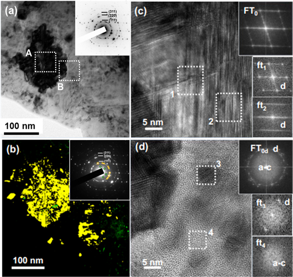
Figure 5. (a) Bright field TEM micrographs of NCD/SiO2/Si films with SAED shown as inset and (b) composed dark field TEM micrographs TEM micrographs corresponding to (a); HRTEM image of (c) selected area A and (d) selected area B designated in (a), respectively. The FT0c and FT0d images are fourier-transformed diffractogram corresponding structure images in 'c' and 'd', respectively, whereas the ft1 to ft4 images correspond to areas 1 to 4, respectively.
Download figure:
Standard image High-resolution imageFigure 6(a) shows the (BF) TEM micrograph of UNCD/SiO2/Si films, revealing that these films consist of some diamond aggregates of size around tens of nanometers evenly dispersed in the matrix of ultrasmall diamond grains with size around 5 nm. Inset in figure 6(a) shows that the SAED pattern of UNCD film depicts ring-shaped diffraction patterns corresponding to (111), (220), (311) diamond lattice planes. It indicates that diamonds grains in these films are ultra-small is size and are randomly oriented. Figure 6(b) shows the c-DF image of these films, which demonstrates the even distribution of diamond aggregates among the matrix of nano-sized diamond grains. The HRTEM images of the diamond aggregate (region A, figure 6(a)) and the periphery region (region B, figure 6(a)) were shown in figures 6(c) and (d), respectively. Figure 6(c) reveals that the diamond aggregates contain a large proportion of stacking faults, which is again inferred from the presence of rel-rods in the FT0c-image. The presence of stacking faults in aggregates are further highlighted by the ft1 and ft2 images corresponding to areas 1 and 2 in figure 6(c), respectively. It should be mentioned that the large diamond aggregates in figure 6(c) appear to consist of many small diamond grains (around ∼10 nm) in size agglomerated together, rather than a single large diamond grains as those in figure 4(c) for MCD or figure 5(c) for NCD diamond grains. There still exists large proportion of grain boundaries in the large diamond aggregates, except that the grain boundaries are much thinner. Moreover, these diamond aggregates can be disintegrated easily during the TEM investigation, confirming that they are the soft agglomeration of ultra-small diamond grains. In contrast, figure 6(d) indicates that the periphery region (region B, figure 6(a)) consists of ultra-small diamond grains, which is inferred from the presence of the ring-shaped diffraction spots in FTod-image corresponding to entire structure image in figure 6(d) and is highlighted by ft3 and ft4 images corresponding to areas 3 and 4 of figure 6(d), respectively. Again, replacing the SiO2/Si by soda-lime glass substrates for growing UNCD films does not alter the granular structure of the UNCD films (supplementary information, figure S3). Notably, the granular structure of UNCD/SiO2/Si (or UNCD/soda-lime glass) films illustrated in figure 6 is essentially the same as the UNCD films grown on conventional Si substrates. The microstructure of UNCD films is least sensitive to the change in substrate materials.
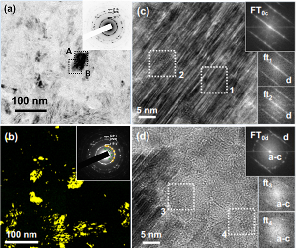
Figure 6. (a) Bright field TEM micrographs of UNCD/SiO2/Si films with SAED shown as inset and (b) composed dark field TEM micrographs corresponding to (a); HRTEM image of (b) selected area A and (d) selected area B designated in (a), respectively. The FT0c and FT0d images are fourier-transformed diffractogram corresponding structure images in 'c' and 'd', respectively, whereas the ft1 to ft4 images correspond to areas 1 to 4, respectively.
Download figure:
Standard image High-resolution imageTo understand the diamond growth behavior on soda-lime glass fibers, the optical emission spectra (OES) of the diamond growth plasmas were collected. It is observed that the species contained in the plasma change with the substrate materials markedly, i.e., a large proportion of substrate materials were ejected from the substrate mixing with the diamond growth plasma. Figure 7(aI) shows that the OES spectrum of MCD/soda-lime glass fiber growth plasma, the CH4/H2, mainly contains H species, which were confirmed by the presence of Hα line at (653.1 nm), Hβ line at (486.1 nm) and Hδ line at 410 nm. Presumably, the H species are the main ingredients, which interact with CH4 to form CH3 radicals, leading to the formation of MCD crystal [38]. In addition, Na (588.9 nm, 819 nm) line of large intensity is observed along with some O (767.7 nm), CO (560.8 nm, 451 nm) and OH (324 nm, 307 nm) lines of smaller intensity, which must have apparently originated from the soda-lime glass substrate via the plasma bombardment. Figure 7(aII) shows that the OES spectrum of MCD/soda-lime glass growth plasma, which is similar with OES of the MCD/soda-lime glass fiber growth plasma, expect that the Na and O-containing species is much smaller, indicating that the soda-lime glass substrates are less susceptible to the bombardment ejection of the species in the substrates. Moreover, The MCD/SiO2/Si growth plasma is similar with OES of the MCD/soda-lime glass growth plasma (not shown) but no Na or O species was observable, indicating that SiO2/Si substrates are rather resistant to the bombardment of plasma ions.
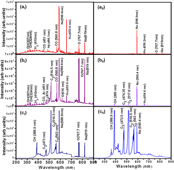
Figure 7. The optical emission spectrum of diamond growth plasmas used for growing (aI) MCD, (bI) NCD and (cI) UNCD on soda-lime glass fibers and those used for growing (aII) MCD, (bII) NCD and (cII) UNCD on soda-lime glass.
Download figure:
Standard image High-resolution imageOn the other hand, the optical emission spectrum of the UNCD/soda-lime glass fibers growth plasma, CH4/Ar shown in figure 7(cI) indicates that these plasma are predominated by C2 dimer emissions at 473 nm, 516.5 nm, and 563 nm along with some CH emission at 388.9 nm, but no H lines were observed. These characteristics are the same as the CH4/Ar plasma used for growing UNCD films on Si substrates. Presumably, the C2 species, which has low energy for forming sp3-bonded carbon, are the species growing diamond nuclei from the a-C matrix. However, when the diamond clusters were formed, they were passivated by the CH species instantaneously that prevents the further attachment of C2 species onto the diamond clusters. Therefore, the diamond grains in UNCD films remained as ultrasmall size (∼5 nm). This plasma also contains Na line at 588.9, 819 nm and O line at 767.7 nm, indicating the presence of large proportion of Na and O species, which were released from soda-lime glass fiber that is the factor which results in totally different morphology of diamond films grown on soda-lime glass fibers, compared with those grown on SiO2/Si or soda-lime glass substrates. Figure 7(cII) shows the optical emission spectrum of the UNCD/soda-lime glass growth plasma, indicating that this plasma is also predominated by C2 dimer and CH emission, but no H lines were observed, except that the Na and O lines are much smaller. Moreover, the OES of UNCD/SiO2/Si growth plasma (not shown) contains only C2 dimer and CH emission. Na and O lines are not observable. Again, the Na and O lines appeared due to ejection from the substrate materials and the soda-lime glass fibers are most susceptible to plasma bombardment that markedly influences the growth behavior of the UNCD films.
The optical emission spectrum of the NCD/soda-lime glass fibers growth plasma CH4/H2/Ar is shown in figure 7(bI), which indicates that this plasma is the mixture of CH4/H2 and CH4/Ar plasma. Both H emissions (at Hα (653.1 nm), Hβ (486.1 nm) and Hδ (410 nm)) and C2 dimer emissions (at 473 nm, 516.5 nm, and 563 nm) are present in this plasma. The CH species, which are usually present together with the C2 species in CH4/Ar plasma are too few to be detectable in CH4/H2/Ar plasma. Although abundant C2 species were present in CH4/H2/Ar plasma, which are expected to nucleate diamond clusters efficiently as in the case of CH4/Ar plasma (the UNCD growth plasma), there is no sufficient CH species in CH4/H2/Ar plasma for passivating the diamond clusters. Moreover, the presence of H species in this plasma can efficiently remove the attached CH species, preventing the passivation effect of hydrocarbons. Therefore, the C2 species can be attached to the diamond clusters continuously enlarging the size of NCD grains. This facilitated the growth of NCD diamond grains to large size. The CH4/H2/Ar plasma also contains Na line at 588.9 and 819 nm and O line at 767.7 nm. Again, both the OES of the NCD/soda-lime glass (figure 7(bII)) and NCD/SiO2/Si (not shown) growth plasma is similar to those of NCD/soda-lime glass fibers growth plasma but with the fewer (or no) Na and O lines, which depends on the susceptibility of the substrate materials to the plasma bombardment damage. The presence of Na and O species are apparently the main factor resulting in a very different granular structure for NCD/soda-lime glass fibers compared with those for NCD/soda-lime glass (or NCD/SiO2/Si) films. The unintentionally added oxygen in growth plasma is expected to result in less sp2-bonded carbon or a-C phase, by privileged etching of non-diamond and leads to the growth of high purity diamond clusters on soda-lime glass fibers [39]. Moreover, the Si species were expected to be released from soda-lime glass fibers and were incorporated into diamond films, creating SiV centers. The presence of Na seems to have a smaller effect on altering the granular structure of the films.
3.2. PL spectroscopy results
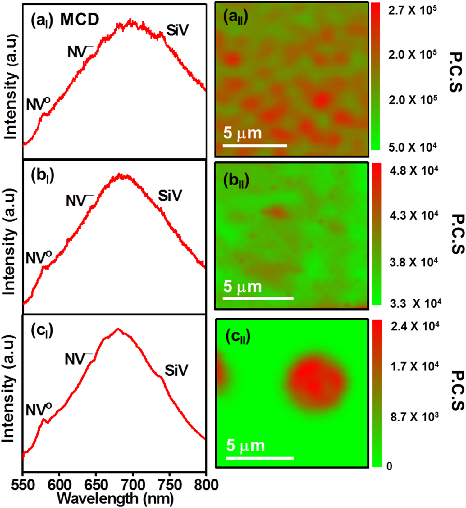
The study on the growth behavior of diamond films using various kinds of growth plasmas and substrates are useful in the tuning of PL emission properties of SiV or NV centers in diamond. Figures 8(aI), (bI), and (cI) show the PL spectrum of MCD/SiO2/Si, MCD/soda-lime glass and MCD/soda-lime glass fibers, respectively, inferring the presence of the NV center's signature, the zero phonon lines (ZPLs) at 575 nm and 637 nm for NV° and NV− respectively, and large PSBs appears beside these ZPLs [9, 14]. In addition, the characteristic ZPL of SiV center was observed at a wavelength of 737.3 nm [14], which completely overlaps with the PSBs of NV center. PL mapping was carried out on these diamond films in order to find the color center's density and distribution. The PL mapping of MCD/SiO2/Si, MCD/soda-lime glass and MCD/soda-lime glass fibers are shown in figures 8(aII), (bII) and (cII), respectively. The resultant mapping reveals the evenly distributed high density of NV and SiV center's luminescence with maximum photon count rate of 2.7 × 10⁵ s−1 for MCD/SiO2/Si films (figure 8(aII)), 4.9 × 10⁴ s−1 for MCD/soda-lime glass films (figure 8 (bII)) and 2.4 × 10⁴ s−1 for MCD/soda-lime glass fibers (figure 8(cII)). While the morphology of MCD films changes markedly with the substrate materials, the characteristics of PL spectra of the three films are essentially the same. However, the photon count rate decreased when SiO2/Si substrates were changed to soda-lime glass and further decreased for MCD/soda-lime glass fibers that can be ascribed to the photon quenching due to the presence of the grain boundary phase and in turn is related to the decrease in grain size.

Figure 8. PL spectrum of MCD films grown on (aI) SiO2/Si, (bI) soda-lime glass and (cI) soda-lime glass fibers. (aII), (bII), (cII) the PL mapping (550–800 nm) of the films corresponding to (aI), (bI), (cI), respectively.
Download figure:
Standard image High-resolution imageThe optical properties of NCD films are very similar to those of MCD films. Figures 9(aI), (bI) and (cI) show the PL spectrum of NCD/SiO2/Si substrates, NCD/soda-lime glass and NCD/soda-lime glass fibers, respectively. As like MCD films, NCD films also exhibits the characteristics of NV and SiV centers with large NV's PSBs. The decrease in grain size from hundreds of nanometers in MCD films to tens of nanometer in NCD films renders the SiV emission more clearly observable. PL mapping of NCD films show the maximum photon count rate of 1.7 × 10⁵ s−1 for NCD/SiO2/Si films (figure 9(aII)), and 6.0 × 10⁴ s−1 for NCD/soda-lime glass films (figure 9(bII)) and 2.0 × 10⁴ s−1 for NCD/soda-lime glass fibers films (figure 9(cII)). Again, the photon count rate decreased by changing the substrates materials from SiO2/Si to soda-lime glass and then to soda-lime glass fibers that are, again, closely related to the PL quenching effect owing to the decrease in grain size. These PL and PL mapping for NCD films are very similar with those of MCD films, regardless of the substrate used for growing the diamond films.
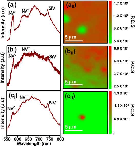
Figure 9. PL spectrum of NCD films grown on (aI) SiO2/Si, (bI) soda-lime glass and (cI) soda-lime glass fibers. (aII), (bII), (cII) the PL mapping (550–800 nm) of the films corresponding to (aI), (bI), (cI), respectively.
Download figure:
Standard image High-resolution imageIn contrast, figures 10(aI) and (bI) show the PL spectra of UNCD/SiO2/Si and UNCD/soda-lime glass films, respectively, indicating that the NV center's PSBs are markedly suppressed, while the SiV center appears with characteristic ZPL at 739 nm. However, large PSB from NV centers is still observable as background, indicating the existence of some NV centers and lowering in NV centers luminescence is probably due to quenching. Figures 10(aII) and (bII) show the PL mapping of UNCD/SiO2/Si and UNCD/soda-lime glass films, which reveals the maximum photon count rate of 3.4 × 10⁵ s−1 and 5.5 × 10³ s−1, respectively. The suppression of NV center's luminescence are apparently owing to the change in granular structure, i.e., the decrease in grain size from hundreds of nanometers in MCD films to around 5 nm in UNCD films. The change of substrate materials from SiO2/Si to soda-lime glass seems to have less effect on modifying the PL properties of UNCD films. However, the UNCD films grown on soda-lime glass fibers show entirely different optical properties from those grown on planar substrate (i.e., SiO2/Si or soda-lime glass substrates). The NV luminescence is completely not observable in the PL spectrum of UNCD films grown on soda-lime glass fibers as shown in figure 10(cI). The SiV center emission is observed at the wavelength of 738 nm with very small PSB. The corresponding PL mapping shown in figure 10(cII) reveals the photon count rate of 7.8 × 10⁴ s−1 for the UNCD/soda-lime glass fibers. Further, the spectral features of SiV such as ZPL width were estimated from the PL spectrums of UNCD samples, i.e., the UNCD films grown on SiO2/Si, soda-lime glass, and soda-lime glass fibers, the estimated ZPL widths are 17.3 nm, 8.8 nm, and 9.4 nm respectively (table 2). It should be noted that, the MCD or NCD samples do not shown clear emission peak, and therefore estimation of ZPL width is not possible.
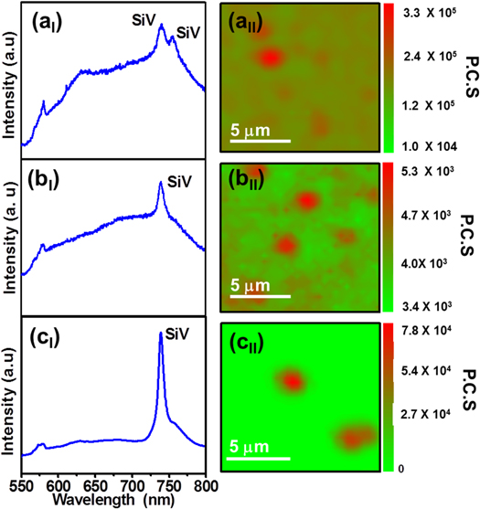
Figure 10. PL spectrum of UNCD films grown on (aI) SiO2/Si, (bI) soda-lime glass and (cI) soda-lime glass fibers. (aII), (bII), (cII) the PL mapping (550–800 nm) of the films corresponding to (aI), (bI), (cI), respectively.
Download figure:
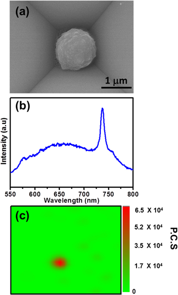
Standard image High-resolution imageThese observations indicate that among the diamond films with different granular structure, only UNCD/soda-lime glass fiber samples show the clear SiV center's emission without the interference of NV center's PSBs. These samples were thus further processed to fabricate the SiV-UNCD particulates. The SiV-UNCD/soda-lime glass fiber samples were immersed in DI water and ultrasonicated for 5 min to release the SiV-UNCD particulates. Subsequently, these SiV-UNCD particulates containing DI water was spread over the SiO2/Si substrate containing inverted pyramidal cavities for better collection of SiV-UNCD particulates. The fabrication process of inverted pyramidal cavities on Si-substrates is reported elsewhere [40]. The SiV-UNCD particulates with the size of 1 μm were settled inside the Si inverted pyramid as shown in figure 11(a). The PL spectrum of SiV-UNCD particulates is shown in figure 11(b), which reveals a sharp ZPL of SiV at a wavelength of 737 nm, similar to those of UNCD/soda-lime glass fibers. In addition, PL mapping performed on the SiV-UNCD particulates located inside the Si inverted pyramidal cavities shown in figure 11(c), revealing the photon count rate of 6.5 × 10⁴ s−1. The photon count rate of SiV-UNCD particulates is the same as those obtained from UNCD particulates on soda-lime glass fibers, that is, the freestanding SiV-UNCD particulates exhibit the similar brightness of SiV emission as those from UNCD/soda-lime glass fibers. The PL spectrum of SiV-UNCD shows the broadening of ZPL emission, which is attributed to the electron–phonon scattering due to the presence of abundant defects.
Figure 11. (a) SEM image, (b) PL spectrum and (c) PL mapping of UNCD nano-particulates located in Si inverted pyramidal cavities.
Download figure:
Standard image High-resolution image
4. Discussion
The above described results indicate that the granular structure of the diamond films imposed a marked effect on the luminescence characteristics of the diamond materials. Both the MCD and NCD films show prominent NV, and weak SiV luminescence, whereas the UNCD films show only significant SiV luminescence. Generally, the crystalline energy of diamond favors the formation of NV center on the surface rather than inside the core of diamond [41–43]. Therefore, the NV center luminescence is strongly correlated with the size of diamond crystals in the films. Although some reports have observed NV center luminescence in NDs with the size of sub-10 nm. Most of the studies observed that the optimum diamond crystal size for the existence of NV center is beyond 40 nm and the most anticipated crystal size is around 60–70 nm [11–14, 17, 18, 44]. The crystal size of the diamond is around ∼500 nm for MCD films and ∼150 nm for NCD grains, which are far larger than this range. Therefore, the presence of NV luminescence cannot be effectively suppressed via the change in granular structure from MCD to NCD films. The wide PSBs of NV centers in diamond arises due to a prominent interaction of NV defects with diamond lattice (electron–phonon coupling) [45–47]. The increases in the proportion of grain boundaries only resulted in marked quenching of NV luminescence.
There are two unique features of UNCD films observed in this study, firstly the diamond grains in the UNCD films are extremely small (∼5 nm, see figure 6). The N species tend to sit on the surface of diamond crystals that hindered the formation of NV center [41–43]. Secondarily, the diamond grains in UNCD films actually consist of sp2-bonded carbon, surrounding the diamond core, which is sp3-bonded carbon, i.e., there exist an interface layer for every diamond grains [48]. The presence of such an interface tends to trap the N-species, preventing the N species to substitute in the diamond lattice to produce the NV centers. Notably, such an interface layer is formed due to the unique formation mechanism of UNCD grains, i.e., the nucleation of diamond clusters from C2 species and passivation by CH species, which is present in the CH4/Ar growth plasma (see figures 7(cI) and (cII)). Consequently, the luminescence from NV centers has been effectively suppressed for UNCD/soda-lime glass fibers. However, in UNCD/SiO2/Si (and UNCD/soda-lime glass) films, the NV centers can be formed since some large diamond aggregates were induced via the coalescence of ultrasmall diamond grains, that is evidence by the TEM micrograph in figure 6. Only when the UNCD films were grown on soda-lime glass, the presence of large diamond aggregates has been completely circumvented and the existence of NV centers can be fully suppressed.
Although, it has been reported that SiV can exist in molecular size diamond to micron size diamond [21, 23], in the present study, bright and clear SiV emission has been observed only for UNCD films with ultrasmall diamond grains (5–10 nm). The brightness of SiV emission decreased markedly for MCD (500 nm) and NCD (80 nm) grains. It seems to contradict to the recently reported studies, which states that MCD shows the better emission than other kind of diamond due to less defective structure [32]. However, our observations are in accord with a study, which reported that the SiV emission enhances with reduction of diamond grain size and maximum intensity has been observed for a diamond grain size of 180 nm [35], it was explained by the assumption that the defects in diamond can enhance with decrease in grain size [35]. Therefore, the bright and clear SiV emission observed for UNCD spherical particulates in the present study can be ascribed to the low defect density for UNCD/soda-lime glass fibers. Moreover, it should be mentioned that for the bio-marking applications, one could need fluorescent diamond with the size of lower than 10 nm, with bright and clear SiV emission, but without the interfering of other emission centers, such as NV center [20]. In this study, this criterion has been satisfied for UNCD spherical particulates by exhibiting the clear SiV emission without interference from NV center. However, the size of the particulates is large, around 1 µm. Nevertheless, these UNCD particulates consists of 5–10 nm ultrasmall diamond grains. It is expected that one can attain ultrasmall particulates by grinding process for reduction of particulate size, in order to employ in bio-marking applications [35].
5. Conclusions
The SiV incorporated UNCD particulates have been fabricated with bright SiV luminescence at 738 nm. For this purpose, initially, three different diamond growth plasmas were employed in the growth of diamond films with different granular structure, including MCD, NCD and UNCD films on three different silicon oxide substrates. PL studies revealed that MCD and NCD films contain both the NV and SiV centers, along with large PSBs, regardless of the substrate materials. The luminescence of NV centers and the associated PSBs were effectively suppressed in UNCD films. Moreover, the abundance of grain boundary phase in UNCD films leads to the quenching of NV luminescence. The quenching effect was less significant for SiV luminescence. Therefore, in UNCD materials with ultrasmall grain size the high fraction of grain boundaries, and brighter SiV luminescence was observed. These results indicate the possibility of size dependent formation of NV centers but not SiV centers. The UNCD on soda-lime glass fibers leads to the formation of SiV-UNCD spherical particulates, which exhibit SiV luminescence with photon count rate of 6.5 × 10⁴ s−1. Micron-sized SiV-UNCD particulates with the same high photon count rate were transferred from soda-lime glass fibers to inverted pyramidal cavities fabricated on Si substrates by the simple crushing of fibers in deionized water and ultrasonication. Such SiV-UNCD particulates with strong emission have great potential for practical applications (micron size particulates can be grinded to make nanometer size particles) in bio-marking and weak magnetic field sensing.
Acknowledgments
The authors would like to thank the Ministry of Science and Technology, Republic of China, for the support of this research through the project No. MOST 104-2112-M-032-003.