

Abstract
MXene, an ultra-thin two-dimensional conductive material, has attracted considerable interest in various fields due to its exceptional material properties. In particular, Ti3C2Tx MXene exhibits distinct optical properties, enabling it to support surface plasmons in the shortwave infrared (SWIR) region. However, it is challenging to enhance the field confinement of MXene surface plasmons in a single-interface structure due to the substantial intrinsic absorption of Ti3C2Tx MXene. Herein, we explore various multilayer structures capable of supporting high field confinement of Ti3C2Tx MXene plasmons, including insulator–MXene–insulator (IMI), MXene–insulator–MXene (MIM), and insulator–MXene–insulator–MXene (IMIM) configurations. We observe that the field confinement of MXene plasmons improves as the thickness of either the MXene or insulator layers decreases, which is attributed to the strong coupling between plasmons at the multilayer interfaces. Furthermore, the IMIM structure demonstrates the most substantial enhancement in field confinement. In an IMIM structure with a 1.3 nm-thick MXene monolayer and a 1.0 nm thick SiO2 layer, the wavelength and effective field size of the plasmon at a frequency of 150 THz (λ0 = 2.0 μm) are calculated to be 24.61 nm and 1.50 nm, respectively. These values demonstrate a reduction by factors of 55 and 596, respectively, compared to those obtained in a single SiO2–MXene interface structure. Multilayer-based MXene plasmons provide a solution for enhancing the field confinement of MXene plasmons in the SWIR region, and we expect them to play a crucial role in a variety of 2D material-based SWIR plasmonic applications.
Export citation and abstract BibTeX RIS
1. Introduction
Two-dimensional (2D) MXenes, a family of transition metal carbides or nitrides, have recently garnered significant interest due to their unique properties, such as outstanding electrical conductivity [1, 2], high mechanical strength [3], and electrochemical performance [4, 5], even with their ultra-thin structures. These attributes have spurred research across diverse applications, such as energy storage [5, 6], electromagnetic shielding [7, 8], gas sensors [9, 10], saturable absorbers [11], and transparent electrodes [12, 13]. Among the various types of MXenes, Ti3C2Tx MXene exhibits unique optical properties, revealing metallic characteristics in the shortwave infrared (SWIR) range that are challenging to observe in other traditional 2D materials, and these properties facilitate the formation of surface plasmons in the SWIR region. Certainly, traditional conductive 2D materials like graphene and black phosphorus support surface plasmons as well [14–19]; however, their relatively low electron density has limited them to the terahertz to mid-infrared frequency ranges [14, 15]. This spectral limitation has impeded the direct implementation of 2D material-based plasmonic applications, including biomolecular sensors [14, 17], optical modulators [20], and metasurfaces [21], in communication wavelength regions such as SWIR. In contrast, Ti3C2Tx MXene, possessing a high electron density, has been reported to exhibit plasma frequencies within the 280–300 THz range, allowing for the excitation of surface plasmons across the full SWIR spectrum. Nevertheless, Ti3C2Tx MXene plasmons show considerably lower field confinement in a structure with a single interface compared to other plasmons, owing to substantial intrinsic absorptions stemming from the high imaginary permittivity of Ti3C2Tx in the SWIR region. For this reason, MXene plasmons have been primarily employed as broadband SWIR absorbers [22]. To effectively employ 2D MXene-based SWIR plasmons in diverse applications, it is necessary to find a method that enhances the field confinement of these plasmons.
In this study, we investigate various multilayer structures that enhance the field confinement of Ti3C2Tx MXene plasmons in the SWIR region. We began by conducting experimental measurements of the optical permittivity of Ti3C2Tx and used these values to analytically calculate the characteristics of MXene plasmons in different multilayer configurations, including insulator–MXene–insulator (IMI), MXene–insulator–MXene (MIM), and insulator–MXene–insulator–MXene (IMIM) structures. Among these structures, we discovered that the IMIM structure exhibited the strongest confinement of MXene plasmon fields, which intensifies as the thickness of MXene or insulating layer decreased. For an MXene plasmon with a frequency of 150 THz (λ0 = 2.0 μm), the wavelength and effective field size in an IMIM structure with a 1.3 nm-thick MXene monolayer and a 1 nm-thick SiO2 insulator layer were calculated to be 24.61 nm and 1.50 nm, respectively. These values exhibit a reduction by factors of 55 and 596, respectively, compared to those obtained in a single SiO2–MXene interface structure.
2. Surface plasmons in insulator–MXene (IM) structure
We experimentally obtained the optical permittivity of Ti3C2Tx
MXene and carried out a theoretical analysis of MXene plasmons based on the acquired data. To measure the permittivity, we prepared a 10 nm-thick Ti3C2Tx
MXene film on a quartz substrate using a two-step process [see Methods]: (1) creating a Ti3C2Tx
MXene solution using the minimum intensity layer delamination (MILD) method, which selectively etches the 'A' layer from the MAX phase (Ti3AlC2), and (2) spin-coating the MXene solution onto the quartz substrate, resulting in a thin Ti3C2Tx
MXene layer. As illustrated in the cross-sectional transmission electron microscopy (TEM) image in figure 1(a), multiple uniform MXene monolayers, each 1.3 nm thick, are stacked atomically thin with air gaps in between, ultimately composing a 10 nm-thick film [23]. Then, we measured the permittivity ( = ' + ''i) of the prepared Ti3C2Tx
MXene film for the frequency (f = ω/2π) range of 50–300 THz using two different ellipsometers: the IR-VASE Mark II (J.A. Woollam) for the 50–176 THz range, and the M-2000 Ellipsometer (J.A. Woollam) for the 176–300 THz range. As shown in figure 1(b), the plasma frequency (fp) where ' = 0 was measured to be 288 THz, and Ti3C2Tx
MXene exhibited metallic properties (' < 0 and '' > 0) in the entire shortwave infrared (SWIR) region below fp. The measured permittivity was fitted using a Drude model (
=
∞–ω0
2
/
ω(ω+ γi)) for analytical calculations, where the parameters ∞, ω0, and γ were determined to be 11.35 +5.11i, 4.08 eV, and 0.219 eV, respectively. We additionally measured for Ti3C2Tx
MXene films with various thicknesses ranging from 2 nm to 1 μm. The results revealed that both ' and '' exhibited similar values with a variation of approximately ±5% and ±1%, respectively, compared to the values measured for the films with a thickness of 10 nm.
= ' + ''i) of the prepared Ti3C2Tx
MXene film for the frequency (f = ω/2π) range of 50–300 THz using two different ellipsometers: the IR-VASE Mark II (J.A. Woollam) for the 50–176 THz range, and the M-2000 Ellipsometer (J.A. Woollam) for the 176–300 THz range. As shown in figure 1(b), the plasma frequency (fp) where ' = 0 was measured to be 288 THz, and Ti3C2Tx
MXene exhibited metallic properties (' < 0 and '' > 0) in the entire shortwave infrared (SWIR) region below fp. The measured permittivity was fitted using a Drude model (
=
∞–ω0
2
/
ω(ω+ γi)) for analytical calculations, where the parameters ∞, ω0, and γ were determined to be 11.35 +5.11i, 4.08 eV, and 0.219 eV, respectively. We additionally measured for Ti3C2Tx
MXene films with various thicknesses ranging from 2 nm to 1 μm. The results revealed that both ' and '' exhibited similar values with a variation of approximately ±5% and ±1%, respectively, compared to the values measured for the films with a thickness of 10 nm.

Figure 1. Surface plasmons in insulator(air)–MXene (IM) structure. (a) A cross-sectional TEM image of a 10 nm-thick Ti3C2Tx
MXene (left) and its schematic view (right). (b) The blue (') and red ('') solid lines show the real and imaginary parts of the measured permittivity of Ti3C2Tx
MXene, respectively. (c) The dispersion relation of MXene plasmon in air–MXene structure, where the gray region indicates the forbidden band in which plasmon is not supported. The inset shows the effective refractive index (neff) of plasmon in air–MXene structure with respect to wavelength. (d) The distribution of magnetic (Hy
) and electric (Ez
) field profiles on the air–MXene interface propagating along the x-axis at a frequency of 150 THz (λ0 = 2.0 μm), calculated using the MATLAB software.
Download figure:
Standard image High-resolution imageFigure 1(c) illustrates the calculated dispersion relation of surface plasmons generated at the interface between air and MXene, assuming that the MXene layer is sufficiently thick. The calculation was conducted using the relation kx
2 = k0
2(MXene)/(1 + MXene) [24], where kx
represents the wavenumber in the propagation direction x, k0 denotes f
/
c, and MXene refers to the measured permittivity of MXene. The surface plasmon frequency (fsp = fp/√2) is calculated to be 202 THz, and kx
displays a slight increase compared to k0 in the SWIR range below fsp, indicating that the plasmons are confined to the air-MXene interface. The effective refractive index (neff = kx
/k0) was calculated to be 1.013 for f = 150 THz (λ0 = 2.0 μm). Figure 1(d) illustrates the field distribution of the surface plasmon propagating along the air–MXene interface at a frequency of 150 THz. The measured effective wavelength of 1974 nm agrees well with the calculated value of λsp (= λ0/neff), where neff is 1.013 as shown in figure 1(c). Despite the high |'| value of Ti3C2Tx
MXene, the surface plasmon exhibits a low effective refractive index due to the relatively high '' value. A low neff implies that the energy of MXene plasmons is predominantly concentrated in the air region, resulting in weak field confinement. This is further confirmed by the notably weakened field confinement observed in figure 1(d), indicating that the majority of the fields exist within the air region with a noticeable lack of such fields within the MXene. To effectively utilize MXene plasmons in plasmonic applications requiring high optical density, it is crucial to enhance their field confinement. Consequently, we explored various multilayer MXene structures with the goal of enhancing the field confinement of MXene plasmons.
3. Plasmonic properties in IMI structures
To investigate the behavior and properties of plasmons in multilayer structures, we employed a theoretical formalism [25, see Methods] and conducted calculations. We applied boundary conditions at each interface to calculate the dispersion relations and field distributions of plasmons in the multilayer structures. Using the calculated solutions, we derived and analyzed four factors that pertain to the field confinement and absorption losses—plasmon wavelength (λsp), propagation length (D), and effective modal and field sizes (Le and Lf) [24–26, see Methods].
The thin MXene layer synthesized on a quartz substrate inherently exhibits a multilayer configuration consisting of insulator (air)–MXen–insulator (SiO2) (IMI). This multilayer structure can enhance the field confinement through the interaction between plasmons generated at the two interfaces (air–MXene and MXene–SiO2 interfaces), depending on the thickness of the MXene layer. When the distance between the two interfaces exceeds the decay length into the MXene layer, the surface plasmons at both interfaces weakly couple, causing the fields to behave independently. This leads to a field distribution similar to that of a single interface, as depicted in figure 1(d). However, when the MXene layer is sufficiently thin, the surface plasmons at both interfaces can strongly couple, resulting in enhanced field confinement [27]. Figure 2(a) illustrates the |Ez | field distribution of 150 THz plasmons for MXene layer thicknesses (hm) of 100, 50, 20, and 10 nm. In structures with MXene layers of 100 and 50 nm thicknesses, the plasmon fields at the two interfaces weakly couple with each other and predominantly expand into the air and SiO2 directions. However, in structures with thin MXene layers of 20 and 10 nm thicknesses, the plasmons at the two interfaces couple more effectively, leading to a stronger confinement of fields near the MXene layer and a more symmetric field distribution with respect to the MXene layer.
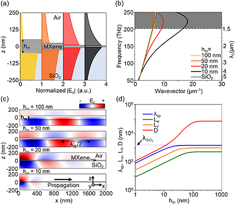
Figure 2. Plasmonic properties in insulator(air)–MXene–insualtor(SiO2) (IMI) structure. (a) |Ez | field distribution of the plasmon mode in the IMI structure at a frequency of 150 THz, where MXene thicknesses (hm) are 100, 50, 20, and 10 nm. (b) Dispersion relations of the plasmon modes in the IMI structure with hm of 100 nm (yellow), 50 nm (orange), 20 nm (red), and 10 nm (black). (c) Ez field profiles of the IMI plasmon mode propagating along the x-direction, calculated using the MATLAB software. (d) Calculated values of plasmon wavelength λsp (blue), effective modal size in terms of energy density, Le (green), effective field size in terms of |E|2, Lf (yellow), and propagation length D (red) as a function of hm, ranging from 1 to 1000 nm. λSiO2 represents the wavelength of light in SiO2.
Download figure:
Standard image High-resolution imageFigure 2(b) illustrates the calculated dispersion relations of surface plasmons in air-MXene-SiO2 multilayer structures with different values of hm, covering a frequency range of 50–250 THz. In all structures, the effective refractive index (neff) of plasmon mode is greater than the refractive index of SiO2 at frequencies below fsp, indicating vertical field confinement. Furthermore, as the MXene layer becomes thinner, the plasmon mode has a higher kx value, corresponding to a larger neff. For plasmons at a frequency of 150 THz (λ0 = 2.0 μm), the neff values are calculated to be 1.47, 1.48, 1.74, and 2.78 for hm values of 100, 50, 20, and 10 nm, respectively. The increase in neff for structures with thin MXene layers is attributed to the strong interaction between plasmons at the two MXene-insulator interfaces. This enhanced interaction increases kx of the MXene plasmon mode, which directly influences the degree of field confinement and localization. In other words, a larger kx indicates a stronger confinement of the electromagnetic field and a more localized plasmon mode within the MXene layer. At frequencies above fsp, quasibound leak modes that exhibit significant propagation losses are observed [24].
Figure 2(c) displays the Ez field distribution of MXene plasmons propagating in the x-direction at 150 THz for structures with hm values of 100, 50, 20, and 10 nm. The figure reveals that as hm decreases, both the plasmon wavelength (λsp) and the effective modal and field sizes (Le and Lf) are reduced. Additionally, the propagation length (D) also decreases as more energy is concentrated in the MXene absorption layer with decreasing hm. For the structure with hm = 10 nm, λsp, Le, Lf and D are calculated to be 719.27 nm, 79.40 nm, 257.05 nm, and 1215.07 nm, respectively, at a frequency of 150 THz (λ0 = 2.0 μm). To quantify the dependence of plasmon properties in the IMI multilayer structure on hm, we calculated λsp, Le, Lf, and D for hm ranging from 1 to 1000 nm at a frequency of 150 THz and plotted the results in figure 2(d). As shown in this figure, the plasmonic properties undergo a rapid change as hm decreases below 100 nm. As hm decreases from 100 to 1 nm, λsp decreases by a factor of 17.22 from 1353.59 nm to 78.64 nm. In addition, Le decreases by a factor of 55.63 from 473.45 nm to 8.48 nm. Likewise, Lf also decreases by a factor of 34.36 from 896.52 nm to 26.09 nm, reflecting an increase in field confinement by more than 30 times in terms of the square of field amplitude. It is worth noting that in the IMI structure, Lf tends to be larger than Le. Additionally, D also significantly decreases to 114.6 nm when hm decreases to 1 nm, indicating limitations in utilizing MXene plasmons as a waveguide. These findings clearly demonstrate that the multilayer structure can have a significant impact on plasmonic properties, particularly on the field confinement characteristics.
4. Plasmonic properties in MIM structures
The metal–insulator–metal plasmonic structure has been a subject of extensive research for decades due to its ability to create a gap plasmon within the insulator spacer, resulting from the interaction between surface plasmons at the two metal surfaces. Decreasing the thickness of the insulating spacer can confine the plasmon field, which in turn enhances its intensity, and this compression can theoretically be infinite [28]. Similarly, in an MXene–insulator (SiO2)–MXene (MIM) multilayer structure composed of two thick MXene layers separated by a nanometer-thick insulating layer, MXene plasmons can be confined within a very thin SiO2 spacer, which is expected to enhance the field confinement. Figure 3(a) illustrates the variation of |Ez | distribution in the MIM structure as the SiO2 thickness is decreased. This figure clearly displays the strong compression and confinement of the electric field within the SiO2 spacer. Figure 3(b) presents the calculated dispersion relations of MXene plasmons in the MIM structure for SiO2 spacer thicknesses (hs) of 100, 50, 20, and 10 nm in the frequency range of 50–250 THz. It is observed that the plasmon mode in the MIM structure has a higher kx than that in the IMI structure shown in figure 2(b), and the kx of the plasmon increases as the thickness of the SiO2 spacer decreases. At a frequency of 150 THz, the neff of the plasmon is calculated to be 2.11, 2.63, 3.85, and 5.45 for hs of 100, 50, 20, and 10 nm, respectively.
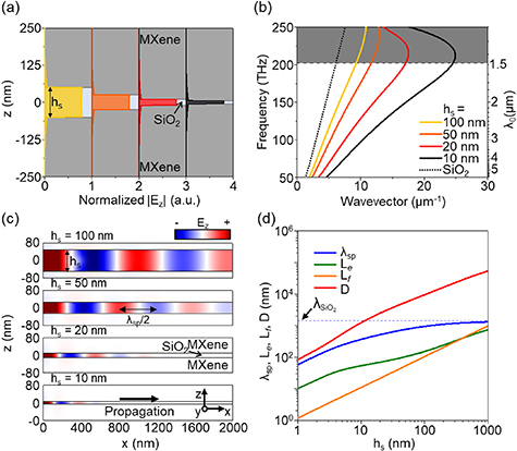
Figure 3. Plasmonic properties in MXene–insulator(SiO2)–MXene (MIM) structure. (a) |Ez| field distribution of the plasmon mode in the MIM structure at a frequency of 150 THz, where SiO2 spacer thicknesses (hs) are 100, 50, 20, and 10 nm. (b) Dispersion relations of the plasmon modes in the IMI structure with hs of 100 nm (yellow), 50 nm (orange), 20 nm (red), and 10 nm (black). (c) Ez field profiles of the MIM plasmon mode propagating along the x-direction, calculated using the MATLAB software. (d) Calculated values of λsp (blue), Le (green), Lf (yellow), and D (red) as a function of hs, ranging from 1 to 1000 nm. λSiO2 represents the wavelength of light in SiO2.
Download figure:
Standard image High-resolution imageFigure 3(c) displays the Ez distribution of a 150 THz frequency plasmon that occurs in the MIM structure at hs values of 100, 50, 20, and 10 nm. In all structures, the plasmon field is compressed into the SiO2 spacer, and the plasmon wavelength decreases with hs. Figure 3(d) shows the values of λsp, Le, Lf, and D of the plasmon mode at a frequency of 150 THz (λ0 = 2.0 μm) as a function of hs in the range of 1–1000 nm. Here, we restricted the minimum value of hs to 1 nm to exclude quantum effects occurring in the MIM structure [29]. As hs decreases, the plasmon field confinement in the MIM structure becomes stronger than that of the IMI structure shown in figure 3(d), and the field confinement in MIM structure is continuously enhanced from 1000 to 1 nm, unlike in the IMI structure. When hs is 10 nm, λsp, Le, and Lf are calculated as 367.19 nm, 53.67 nm, and 10.99 nm, respectively, which are reduced by 1.96, 1.45, and 23.39 times, respectively, compared to the values of the IMI structure with hm of 10 nm. As hs decreases, it is worth noting that Lf becomes progressively smaller than Le, which indicates that the electric fields of plasmon modes are mostly concentrated in the SiO2 spacer. When hs decreases to 1 nm, λsp, Le, and Lf decrease to 58.08 nm, 10.16 nm, and 1.17 nm, respectively. However, due to the strong absorption of MXene, D also decreases to 1246.36 nm and 83.87 nm for hs of 10 nm and 1 nm, respectively, and these values are comparable to those observed in the IMI structure.
5. Plasmonic properties in IMIM structures
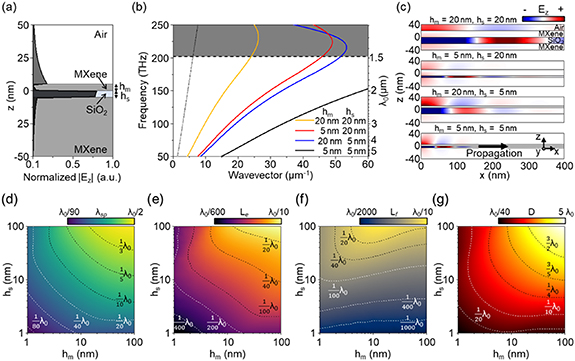
Finally, we investigated the plasmonic properties in an insulator (air)—MXene—insulator (SiO2)—MXene (IMIM) structure, which contains both IMI and MIM structures. Figure 4(a) shows the |Ez | distribution in the IMIM structure with a 5 nm thick MXene layer (hm = 5 nm) and a 5 nm thick SiO2 spacer (hs = 5 nm) on the sufficiently thick MXene substrate. In this structure, we can expect that the field confinement occurs through the plasmonic interactions generated at the three interfaces (air–MXene, MXene–SiO2, and SiO2–MXene interfaces). The plasmon mode in the IMIM structure is confined within the SiO2 spacer between the thin MXene film and the thick MXene substrate, and it also interacts with the counter-phase charge oscillation at the top air–MXene interface, resulting in even stronger field confinement [17, 18]. To observe the plasmonic properties of the IMIM structure, both the thickness of the insulating spacer (hs) and the thickness of the thin MXene film (hm) need to be sufficiently small. When hs is too large, the plasmons exhibit characteristics similar to those of the IMI structure discussed in figure 2, and when hm is too large, they exhibit characteristics similar to those of the MIM structure discussed in figure 3.
Figure 4. Plasmonic properties in insulator(air)–MXene–insulator(SiO2)-MXene (IMIM) structure. The structure is designed with the MXene thin film thickness hm and the SiO2 spacer thickness hs. (a) |Ez | field distributions of the IMIM plasmon mode at a frequency of 150 THz for both hm and hs of 5 nm. (b) Dispersion relations of IMIM plasmons for Case 1 (hm = 20 nm, hs = 20 nm) (yellow), Case 2 (hm = 5 nm, hs = 20 nm) (orange), Case 3 (hm = 20 nm, hs = 5 nm) (red), and Case 4 (hm = 5 nm, hs = 5 nm) (black). (c) Ez field profiles of the IMIM plasmon modes propagating along the x-direction, calculated using the MATLAB software. (d)–(f) calculated λsp, Le, Lf, and D as a function of hm and hs, ranging from 1 nm to 100 nm, respectively.
Download figure:
Standard image High-resolution image
Figure 4(b) shows the dispersion relation of plasmon modes in the IMIM structure for four cases of hm and hs values in the frequency range of 50–250 THz: (Case 1) hm = 20 nm, hs = 20 nm, (Case 2) hm = 20 nm, hs = 5 nm, (Case 3) hm = 5 nm, hs = 20 nm, and (Case 4) hm = 5 nm, hs = 5 nm. In Case 2 and Case 3, the plasmon mode has a larger wavevector compared to Case 1, while Case 4 exhibits a significantly larger wavevector than the other cases. At a frequency of 150 THz, the effective refractive index (neff) of the plasmon mode is calculated to be 5.12, 9.47, 10.65, and 18.48 for Cases 1, 2, 3, and 4, respectively. These results demonstrate that the IMIM structure can provide higher effective refractive index and stronger field confinement than the IMI or MIM structures alone, where both hm and hs should be thin for maximum effectiveness. Figure 4(c) shows the Ez field distributions of plasmons at a frequency of 150 THz (λ0 = 2 μm) in the IMIM structure for the four cases discussed in figure 4(b). It can be observed in Case 4 that there is a significant reduction in λsp and that the field is strongly concentrated within the SiO2 spacer. In Case 4, Le and Lf are calculated to be 47.38 nm and 28.77 nm, respectively. Furthermore, it is observed that Case 2 dominantly exhibits the plasmonic properties of the MIM structure, while Case 3 dominantly exhibits those of the IMI structure.
Figures 4(d)–(g) display the λsp, Le, Lf, and D of the plasmon modes as a function of hm and hs, ranging from 1–100 nm, in the IMIM structure at a frequency of 150 THz (λ0 = 2.0 μm). When hs is fixed at a large value of 100 nm, the IMIM structure becomes similar to the IMI structure. In this case, as hm decreases from 100 to 1 nm, λsp, Le, and Lf decrease by factors of 12.01, 17.21, and 4.08, respectively, and D decreases by a factor of 77.33. Similarly, when hm is fixed at a large value of 100 nm, the IMIM structure becomes similar to the MIM structure. In this case, as hs decreases from 100 to 1 nm, λsp, Le, and Lf decrease by factors of 16.26, 14.53, and 99.73, respectively, and D decreases by a factor of 102.78. When both hm and hs simultaneously decrease from 100 to 1 nm, λsp and Le experience more significant reductions by factors of 43.36 and 45.85, respectively. Lf also significantly decreases by a factor of 67.99, but its value is slightly larger compared to that of the structure with hm = 100 nm and hs = 1 nm, due to the penetration of a portion of the electric field through the thin MXene layer. Additionally, D decreases by a factor of 152.21. When hm is 1.3 nm, corresponding to the thickness of the MXene monolayer, and hs is 1 nm, the λsp, Le, and Lf are calculated to be 24.61 nm, 3.27 nm, and 1.50 nm, respectively. These results clearly demonstrate that the IMIM multilayer structure is the most optimized configuration for confining the field of MXene plasmons.
6. Conclusion
We have demonstrated the strong field confinement of MXene plasmons through the investigation of various multilayer structures. Among the diverse configurations, the IMIM structure proved to be the most effective in confining the plasmon mode, as it combines the plasmonic confinement capabilities of both IMI and MIM structures. Our observations indicate that field confinement is enhanced when the thickness of both MXene and insulator layers are reduced in multilayer structures. With a monolayer MXene thickness of 1.3 nm and a 1 nm thick SiO2 layer between the two MXene layers, the wavelength of the plasmon at a frequency of 150 THz (λ0 = 2.0 μm) in the IMIM structure is reduced to 24.61 nm, and the effective modal and field sizes are reduced to be 3.27 nm and 1.50 nm, respectively. The strong field confinement of MXene plasmons in the IMIM structure offers a solution that transcends the limitations of MXene plasmons, significantly expanding the potential for implementing various 2D MXene-based applications such as subwavelength nonlinear optics, photodetectors, biosensors, metasurfaces, light-emitting devices, and optical modulators in the SWIR region.
7. Methods
7.1. Synthesis of Ti3C2Tx
Ti3AlC2 powder with a size of 40 µm was procured from Carbon Ukraine, while Sigma-Aldrich provided hydrochloric acid (HCl, 37%), and Alfa Aesar provided lithium fluoride (LiF, 98.5%). To synthesize Ti3C2Tx, the MILD method was employed by removing the 'A' layers of the parent MAX phase (Ti3AlC2). In this method, LiF (3.2 g) in 40 ml of 9M HCl was continuously stirred in a polypropylene bottle, and Ti3AlC2 powder (2 g) was gradually added to the solution. The reaction continued at 35 °C for 25 h, and the reacted solution was washed with DI water and centrifuged repeatedly at 3500 rpm for 5 min until the Ti3C2Tx supernatant solution turned dark-green at a pH of around 6. The dispersed solution was centrifuged at 3500 rpm for 30 min to obtain a stable supernatant containing single MXene sheets. To ensure homogenous thickness and dispersibility, the solution was argon-purged and then bath-sonicated for 30 min using an ultrasonic cleaner (LK-U065D, 150W, Korea) with Ar purging. The sonicated solution was then centrifuged at 11 000 rpm for 30 min, the supernatant was removed, and residual paste was dispersed in distilled water. The final dispersion solution, which had a concentration of roughly 45 mg ml−1, was diluted as needed.
7.2. Theoretical formalism
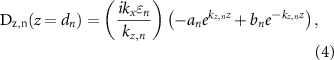
For theoretical calculations of plasmon wavevector kx in multilayered structure, we solved the boundary condition of Maxwell's equations of each interface deriving the continuity of electromagnetic field [24, 25]. Assuming propagation of the wave in the positive x-direction at each interface, the surface plasmons are represented as transverse-magnetic (TM) waves:


The tangential electric field Ex
and normal displacement field Dz
(Ez
) components of the nth interface can be expressed of parallel to x and perpendicular to z:

where dn
is the distance of nth interface from the 1st interface, an
and bn
are the field coefficients, kz,n
is the perpendicular wavevector at the nth interface, and the kx
is defined by the momentum conservation kx
2
= kz,n
2
—n
(ω/c)2 [25], and n
is the permittivity of nth layer. At the nth interface between nth and (n + 1)th layers, the continuity of the tangential electric field and normal displacement field must be satisfied according to the boundary conditions:


In multilayered condition, solving equations (10) and (11) as simultaneous equations can yield the multilayered structure plasmon wavevector kx . Especially, the plasmon wavevector kx in the four layers structure is determined by adopting the determinant of the field coefficient an and bn yielding the plasmon dispersion relation:
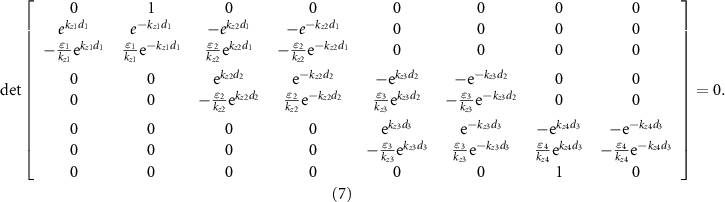
By applying this determinant equation, the plasmon wavevector kx of more complex multilayered structures can be obtained by adding boundary conditions in the matrix that correspond to additional layers.
7.3. Definition of analysis parameters
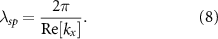
The plasmon wavelength, λsp, which represents the distance between two adjacent intensity maxima of the plasmon mode, can be directly calculated from the real part of kx using equation (8). This parameter serves as a significant metric for characterizing the spatial extent of plasmon field confinement and determining the overall performance of plasmonic devices
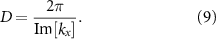
In addition, the propagation length, D, which quantifies the distance over which a plasmon mode can propagate before being significantly attenuated due to absorption losses, can be directly calculated from the imaginary part of kx using equation (9). This parameter is critical for determining the feasibility and efficiency of plasmonic devices based on multilayer structures, as well as for designing strategies to mitigate absorption losses and enhance the performance of the devices
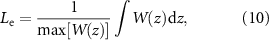
The effective modal size, Le, representing the effective size of the energy distribution of the plasmon mode, can be obtained by calculating the effective size of the energy density (W) using equations (10) and (11) [24]. These parameters reflect the energy confinement of plasmon modes in multilayer structures and are a crucial for optimizing the performance of plasmonic devices, such as sensors, waveguides, and filters
where E and H represent the electric and magnetic fields, respectively, (z) denotes the real part of the permittivity at the specific location z, and μ0 represents the vacuum permeability.
Finally, the effective field size, Lf, can be obtained by calculating the effective size of the square of electric field amplitude (|E|2) using equation (12) [26]. These parameters directly reflect the electric field confinement of plasmon modes in multilayer structures
7.4. Numerical simulation
Acknowledgments
This study was supported by the National Research Foundation of Korea (2020R1A2C2010967, 2022R1A2C3006227, 2021M3H4A1A03047327), Institute for Information & Communications Technology Planning & Evaluation (IITP) Grants (2020-0-00947, 2022-0-00198 and 2022-RS-2022-00164799), National Research Council of Science & Technology (NST) Grants (CRC22031-000 and CAP22051-102), Fundamental R&D Program for Core Technology of Materials (20020855) funded by the Ministry of Trade, Industry and Energy, KIST Institutional Program (2E32801-23-P027), and KU-KIST School Project. Part of this study has been performed using facilities at IBS Center for Correlated Electron Systems, Seoul National University.
Data availability statement
The datasets associated with this research paper are available from the authors upon request.
Author contributions
J K, C M K, and M K K conceived the research project. J K developed the physical concept, conducted theoretical analysis, and measured MXene permittivity. C P contributed to useful discussions and also measured MXene permittivity. H K executed the fabrication and characterization of MXene, while P N R captured the TEM image. All authors participated in discussing the results and writing the manuscript.