
Abstract
Engineering the doping level in graphene is essential to realizing functional electronic and optoelectronic devices. While achieving strong p-doping is relatively straightforward, electrostatic or chemical approaches to negatively dope graphene have yielded electron densities (ns) of −9.5 × 1012 cm−2 or below. In this work, we demonstrate very high ns (−1013 to −1014 cm−2) in graphene, on an ion-exchanged glass substrate, which is widely used in touch screen displays (e.g. smart phones). Moreover, the proposed method, which is easy to implement and scalable, leads to relatively stable graphene doping, with about a 40% increase in sheet resistance over 5 months at ambient conditions.
Export citation and abstract BibTeX RIS

Original content from this work may be used under the terms of the Creative Commons Attribution 4.0 license. Any further distribution of this work must maintain attribution to the author(s) and the title of the work, journal citation and DOI.
1. Introduction
Graphene holds great potential in the future of optoelectronic device applications, owing to its unique transport [1–3], optical [4–6], and mechanical properties [7–9]. However, the expected high performance of graphene is often hindered by the substrate, with, for instance, a relatively high sheet resistance (Rs ) ∼ 1 kΩ sq−1 for graphene on conventional substrates such as SiO2/Si. Much lower values in the order of a few 100 Ω sq−1 are required for industrial touchscreen [10] and transparent conductor [11–14] applications. Ongoing research thus continuously tries to find methods to reduce the resistance of graphene. One method is to increase, through doping, the low charge carrier density (ns ) ∼1–2 × 1012 cm−2 [15–17], that determines, along with the carrier mobility, the resistance of graphene [18].
Graphene doping techniques can be broadly classified in three categories: (i) substitutional, (ii) chemical and (iii) electrostatic. With substitutional doping techniques, the number of heteroatoms incorporated into the graphene lattice is difficult to control which can compromise the accuracy and repeatability of doping level achievable by this method. Meanwhile, chemical doping techniques can suffer from a lack of control over the surface coverage and reactivity of the chemical species adsorbed onto the graphene which can compromise the doping stability and repeatability. Additionally, the incorporation of heteroatoms or chemical dopants can induce lattice stain effects and structural defects, which may compromise the conductivity of graphene thus limiting its use in electronic devices [19]. On the other hand, electrostatic doping, where graphene n- or p- doping is induced by the application of a gate voltage, allows for a degree of reversible and accurate control of the doping. The main issue, however, is the relatively low reachable nS due to the limited capacitance of the available solid-state thin film or electrolyte capacitors (e.g. 300 nm-thick SiO2 grown on Si) and limitations due to the host substrates.
In light of these limitations, several works have demonstrated graphene doping after its transfer onto appropriately treated substrates. For example, the deposition of ammonia or aluminum on the surface onto SiO2 substrates led to formation of positive (NSiO+) and negative (AlSiO-) surface charge layers on the substrate which were shown to induce the electrostatic n- and p-doping of graphene, with nS of −8.62 × 10¹² and 2.17 × 1012 cm−2, respectively [20].
More recently, n-doping of graphene has been demonstrated on multicomponent glass where the mobility of the ions was exploited to n-dope graphene to a level sufficient to reverse environmental and process related p-doping [21]. Similarly, soda lime glass (SLG) has been used to obtain highly n-doped graphene, in the order of −1.33 × 1013 cm−2, where it was proposed that the high surface density of Na in SLG dopes the graphene via electron transfer [22].
In this work we describe, for the first time, a method to obtain highly n-doped graphene with a ns of the order of −1013 to −1014 cm−2 by transferring graphene (e.g. pristine graphene) onto ion-exchanged (IOX) Corning® Gorilla® glass. This glass, depicted schematically in figure 1(a), contains potassium ions (K+) from an ion-exchange process in which some of the sodium ions (Na+) near the glass surface are replaced by K+. The depth of the exchange layer (referred to herein with a subscript) can be modified in the range of 1–50 μm.
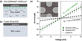
Figure 1. Sketch of graphene transferred onto IOX Corning® Gorilla® glass (a) and FS glass (b) where blue shaded area comprises the silica matrix. The top surface of the IOX Corning® Gorilla® glass contains potassium (K+) from an ion-exchange procedure, where the depth of layer can be modified from 1 to 50 μm; (c) I–V characteristics measured for graphene on IOX20 µm Corning® Gorilla® glass (green circles) and FS (black circles) substrates. For each device, the I–V curve was measured several times to ensure repeatability, sampling at 1 mV steps, which are subsequently averaged. A linear fit was applied to the I–V curves collected for all devices on each substrate (totaling 16 IOX and 16 FS devices), with error bars representing the spread in the data. Note that the error bar for graphene/FS is not visible because of the low standard deviation. The average Rs was obtained from the slope. The inset of the graph shows an optical microscope image of a real sample. Scale bar 100 μm.
Download figure:
Standard image High-resolution image2. Experimental
Two types of devices were fabricated on IOX Corning® Gorilla® glass, fused silica (FS) and Si/SiO2 substrates for electrical measurements. van-der-Pauw devices, shown in figure S1(a) in supplement 1, features four identical devices (D1–D4) with the typical cloverleaf geometry for performing sheet resistance measurements. Hall bar devices, shown in supplemental figure S1(b), features two identical devices (D1 and D2) with Hall bar geometry for performing transport measurements. To allow for statistical descriptions, multiple samples of each design were fabricated. Both devices follow the same fabrication procedure outlined below, with the addition of Al2O3 device encapsulation for the Hall bar structures. The fabrication procedure is shown schematically in supplemental figure S2.
All experiments have been carried out with graphene grown by chemical vapor deposition (CVD) purchased from Graphenea. The graphene sheets were transferred using a wet-transfer technique [23] onto FS, Si/SiO2 or IOX Corning® Gorilla® glass substrates. Prior to graphene transfer, the substrates were cut to a size of 1 cm2 and cleaned in an ultrasonic bath using acetone and isopropyl alcohol for 5 min in each solvent. Then, Ti/Au (3/50 nm) contacts were fabricated with van-der-Pauw or Hall bar geometry by photolithography and lift-off processes. CVD graphene was transferred to the metallized substrates which were subsequently dried under atmospheric conditions for 12 h and later immersed in a bath of acetone to remove the PMMA residues. A photolithography process and subsequent argon/oxygen etching step was performed to reduce the area of the graphene to a 300 μm diameter cloverleaf in van-der-Pauw devices and a 140 × 300 μm rectangle in the Hall bar devices, respectively. Remaining photoresist was removed by immersing the samples in acetone for 2 min. Finally, the Hall bar devices were encapsulated with 40 nm Al2O3 by atomic layer deposition, A final photolithography and subsequent etching process was performed to remove the excess the Al2O3. The etching was performed by dipping the samples in a buffered HF oxide etchant solution (BOE, HF: NH4F, 1:7) for 1 min.
The four-point Rs
of all van-der-Pauw devices (comprising 16 on IOX and 16 on FS) have been measured in a probe station equipped with two precision source-meter units (Keysight B2901). For each device, the I–V curve was measured several times to ensure repeatability, sampling at 1 mV steps, which were subsequently averaged. A linear fit was applied to the I–V curves collected for all devices on each substrate, from which the average Rs
was obtained from the slope according to equation (1), which considers the geometric factor ( /ln(2)) for the cloverleaf geometry to calculate Rs
[24, 25].
/ln(2)) for the cloverleaf geometry to calculate Rs
[24, 25].
The Rs, ns
and μ of the Hall bar devices (comprising 16 on IOX20 μm and 2 on Si/SiO2) was carried out at 300 K in a physical property measurement system by quantum design. A constant DC current of 1 μA was injected into the sample via probes 1–2 whilst probes 3–4 and 3–5 measured the longitudinal (V34) and transverse (V35 (Hall)) voltage, respectively, during a perpendicular magnetic field sweep (−5 T to 5 T) at 300 K. The subscripts indicate the contact pads shown in figure 2(a). From the longitudinal voltage (V34), the sheet resistance (Rs
) was determined at zero magnetic field by Ohms law according to equation (2), where 'W' and 'L' correspond to the width (140 μm) and length (300 μm) of the graphene area, respectively. The charge carrier density (ns
) was obtained from the slope of the linear fit between the transversal voltage (VHall), and the magnetic field (B), according to equation (3) where qe
is the electron charge (1.6 × 10⁻¹⁹ °C) and IDC is the constant DC current, (1 μA). Assuming the Drude model of conductivity [26], the mobility (μ) was calculated by equation (4). Finally, the Fermi level, EF, was calculated from the ns
according to equation (5), where ħ is reduced planks constant, vF
is the Fermi velocity, kF
is Fermi wave vector which is equal to  and ns
= number of additional charge carriers
and ns
= number of additional charge carriers
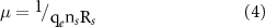

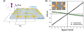
Figure 2. Simplified three-dimensional views of the Hall bar structures, along with circuits for the Hall effect measurement. The heavy purple arrow indicates the direction of the magnetic field corresponding to the circuit diagrams shown. A constant DC current of 1 μA was injected through the sample via probes '1–2' whilst and probes '3–4' or '3–5' to measure the RS or VHall, respectively during a perpendicular magnetic field sweep (−5 T to 5 T) at 300 K. (b) VHall vs. magnetic field (B) data obtained from 16 graphene/IOX1−43 µm devices (green circles) and 2 graphene/Si/SiO2 devices (black circles) where the dotted line represents a linear fitting of all devices.
Download figure:
Standard image High-resolution image3. Results and discussion
Figure 1(c) compares the I–V characteristics for van-der-Pauw devices prepared on IOX20 μm Corning® Gorilla® glass and FS substrates, where the difference in slope confirms the strong influence of the supporting substrate on the sheet resistance of graphene. The corresponding average Rs (obtained from the slope of the linear fit according to equation (1)) of the graphene/FS devices was 1.22 ± 0.353 kΩ sq−1 which is similar to those values previously reported [12], thus confirming the reliability of our transfer technique and characterization method. On the other hand, the Rs for the graphene/IOX20 μm devices was consistently 3–5 times lower with an average of 0.245 ± 0.069 kΩ sq−1. The results were quite repeatable across all devices fabricated by independent runs.
Rs measurements were also performed on graphene transferred onto bare (i.e. with no pre-defined Au contacts) IOX20 μm Corning® Gorilla® glass and FS substrates. Interestingly, and in contrast to Au-contacted graphene devices (figure 1(c)), no difference in Rs was found, irrespective of the underlying substrate with both IOX and FS systems measuring between 1–2 kΩ sq−1 (figure S3 in supplement 1). This result was repeated several times by independent fabrication processes.
Eight samples on IOX1−43 μm were fabricated with a hall bar design, figure S1(b) in supplement 1, where each sample contains two identical devices (D1 and D2) for gathering statistics. Figures 2(a) and (b) show the measurement scheme and the evolution of Hall voltage (VHall) as a function of perpendicular magnetic field sweep (B) between −5 and 5 Tesla at 300 K.
A negative slope indicates n-type doping (excess of electrons), while a positive slope indicates p-type doping (excess of holes) where the magnitude of the gradient correlates to the strength of the doping. Comparing the slope of the devices fabricated on IOX1−43 µm to that of the Si/SiO2 reference, it is found that VHall induced by the charge carriers in the graphene on IOX substrates is lower in amplitude and of opposite sign, for a fixed current and magnetic field.
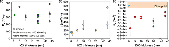
Figures 3(a)–(c) shows the evolution of Rs, µH and ns respectively, for the eight graphene/IOX samples, comprising of IOX thicknesses: 1 × 1 µm, 1 × 5 µm, 2 × 10 µm, 2 × 20 µm and 2 × 43 µm. Each marker and corresponding error bar represent the average and standard deviation of D1 and D2. Identical measurements on the Si/SiO2 reference sample are indicated with blue markers. Note that the low Rs (and high ns) is reproduced with a comparable magnitude irrespective of the IOX thickness.
Figure 3. The evolution of (a) Rs (b) µH and (c) ns with IOX layer thickness. Each marker and error bars represent the average and standard deviation of D1 and D2. Samples included in the statistics are 1 × 1 μm, 1 × 5 μm, 2 × 10 μm, 2 × 20 μm and 2 × 43 μm. In graph (a) purple markers represent the Rs for the IOX devices remeasured after 5 months. The corresponding values for the Si/SiO2 reference sample is provided in the inset of graph a. The values of µH and ns for the Si/SiO2 reference samples are indicated with blue markers in graphs b and c. In some cases, the error bars were smaller than the markers and are not visible.
Download figure:
Standard image High-resolution image
The sheet resistance measurements shown in figure 3(a) show an average Rs values 0.318 ± 0.078 kΩ sq−1 for the of the graphene/IOX1−43 µm devices. This is in close agreement with the Rs statistics obtained with the van-der-Pauw structures (0.245 ± 0.069 kΩ sq−1) and confirms that the effect of the underlying substrate is significant and independent of the slight processing differences between the two designs e.g. encapsulation with Al2O3. Furthermore, the Rs for the Si/SiO2 reference, 2.32 ± 0.690 kΩ sq−1, is of the same order of that for graphene/FS devices fabricated with van-der-Pauw geometry (1.22 ± 0.353 kΩ sq−1).
The room temperature (RT) carrier mobility (µ) measurements, in figure 3(b), show a mobility between 80–800 and 150–160 cm2 V−1 S−1 for graphene on IOX and Si/SiO2 substrates, respectively. Graphene wet-transferred onto Si/SiO2 substrates typically produce mobility values in the range of 102–103 cm2 V−1 s−1 at 300 K for a carrier concentration, ns ∼ 1012cm−2 [12, 16, 27]. In the future, we will perform studies and evaluate previous techniques to reduce the spread of the mobility we have observed toward the highest values observed in the literature for glass [28–30].
The carrier density measurements (ns ) shown in figure 3(c) show a moderate p-doping (average ns +3.9 × 1013 cm−2 ± 1.3 × 1013 cm−2) for the graphene/Si/SiO2 devices (blue marker). The doping may depend on processing conditions and is consistent with data previously reported in graphene − silica systems [17, 31–36]. In contrast, the graphene/IOX1−43 µm devices, indicated with red markers, show a strong n-doping within range −1.7 × 10¹⁴ to −4.5 × 1014 cm−2, with an average of −1.9 × 10¹⁴ ± −9.8 × 1013 cm−2 which validates the effect of the IOX layer on the graphene doping. Substituting the average ns value into equation (5) returns a Fermi level (EF) of −1.61±0.4 eV for the graphene/IOX1−43 µm devices.
The observed high ns might be related to a local surface density of positive charge present in the IOX glass layer in which the graphene is in direct contact. A positive surface charge might originate from the excess of K+ after the ion-exchange process [37, 38]. When the graphene is contacted, electrons are drawn into graphene to neutralize the excess surface charge due to IOX process. Similar examples have been reported in literature where it is demonstrated that a charged substrate surface induces the doping of graphene [20, 39]. Although it is clear that the IOX glass is a key element to achieve doping, additional experiments are needed to confirm the doping mechanism and the interplay between the processing steps to make the devices and the substrate composition [17, 40–42].
To evaluate the stability of the doping, the Rs
of several IOX and Si/SiO2 devices was measured again after being kept for five months in a dry box. The IOX devices (purple markers in figure 3(a)) reveal an increase between 0.100–0.160 kΩ sq−1 corresponding to a 42% average increase as compared to the initial Rs
. The Si/SiO2 devices reveal a similar increase of  0.100 kΩ sq−1, corresponding to a 5% average increase compared to the initial Rs
. Given that the increase in Rs
after 5 months is of a similar magnitude for both IOX and Si/SiO2 devices, we understand that the 42% increase for the IOX is only large in the context that the initial starting Rs
was low. We believe that the increase in Rs
after 5 months is probably not due to the IOX substrate, but more likely related with a combination of atmospheric exposure, which is known to degrade the graphene, and degradation induced by the Al2O3 encapsulation layer. In this regard, future work should consider alternative encapsulation techniques, that maintain an effective moisture barrier and the initial quality of the transferred graphene over time.
0.100 kΩ sq−1, corresponding to a 5% average increase compared to the initial Rs
. Given that the increase in Rs
after 5 months is of a similar magnitude for both IOX and Si/SiO2 devices, we understand that the 42% increase for the IOX is only large in the context that the initial starting Rs
was low. We believe that the increase in Rs
after 5 months is probably not due to the IOX substrate, but more likely related with a combination of atmospheric exposure, which is known to degrade the graphene, and degradation induced by the Al2O3 encapsulation layer. In this regard, future work should consider alternative encapsulation techniques, that maintain an effective moisture barrier and the initial quality of the transferred graphene over time.
3.1. Applications
We strongly believe that the results presented in this work could enable a route towards a host of previously inaccessible applications of graphene where the combination of low sheet resistance strong n-doping and high EF, obtained on a transparent glass substrate, are important. For example, in energy conversion and electron emission applications such as organic light emitting diodes (OLED), light emitting diodes (LEDS), solar cells [43–45]. Secondly, the demonstrated high ns, corresponding to EF of −1.61 eV, could be interesting for plasmonic applications, which for graphene devices has so far been limited to mid-infrared and longer wavelengths [46–49]. As frequency of plasmonic excitation scales according to √EF, the graphene/IOX system could be subsequently nanostructured into, for example, nanodisk or nanoribbon geometries, for making plasmonic devices operating in the near-infrared region.
4. Conclusions
As described herein, IOX Corning® Gorilla® glass was found to naturally modify graphene doping without the need of additional post-treatment (e.g. thermal poling under applied potential). Sheet resistance and Hall measurements performed at RT demonstrate high and reproducible doping levels of graphene placed in direct contact with IOX glass leading to graphene with an unexpectedly high nS (−1013 cm−2 or higher). The negative values obtained with IOX glass were found to be 1–2 orders of magnitude larger than the positive values on undoped silica glass substrate.
Acknowledgments
The authors acknowledge financial support from the Spanish Ministry of Economy and Competitiveness through the 'Severo Ochoa' Programme for Centres of Excellence in R&D (CEX2019-000910-S) [MCIN/ AEI/10.13039/501100011033] and the project TUNA-SURF (PID2019-106892RB-I00), from Fundació Privada Cellex, Fundació Mir-Puig, and from Generalitat de Catalunya through the CERCA programme. This project was also funded by the Agència de Gestió d'Ajuts Universitaris i de Recerca (2021 SGR 01458). This project also received funding from the European Union's Horizon 2020 Research and Innovation Programme under the Marie Skłodowska-Curie Grant Agreement No. 754510.
The authors would like to thank the Low Temperatures and Magnetometry Service of ICMAB-CSIC for assisting and performing the transport measurements under magnetic field on the Physical Properties Measurement System PPMS. We also thank Dr Xiaoju Guo for help with samples.
Data availability statement
All data that support the findings of this study are included within the article (and any supplementary files).
Supplemental-document (0.2 MB DOCX) Highly doped graphene on ion-exchanged glass