
Abstract
Ultrafast charge separation after photoexcitation is a common phenomenon in various van-der-Waals (vdW) heterostructures with great relevance for future applications in light harvesting and detection. Theoretical understanding of this phenomenon converges towards a coherent mechanism through charge transfer states accompanied by energy dissipation into strongly coupled phonons. The detailed microscopic pathways are material specific as they sensitively depend on the band structures of the individual layers, the relative band alignment in the heterostructure, the twist angle between the layers, and interlayer interactions resulting in hybridization. We used time- and angle-resolved photoemission spectroscopy combined with tight binding and density functional theory electronic structure calculations to investigate ultrafast charge separation and recombination in WS2-graphene vdW heterostructures. We identify several avoided crossings in the band structure and discuss their relevance for ultrafast charge transfer. We relate our own observations to existing theoretical models and propose a unified picture for ultrafast charge transfer in vdW heterostructures where band alignment and twist angle emerge as the most important control parameters.
Export citation and abstract BibTeX RIS

Original content from this work may be used under the terms of the Creative Commons Attribution 4.0 license. Any further distribution of this work must maintain attribution to the author(s) and the title of the work, journal citation and DOI.
1. Introduction
The great abundance of high-quality 2D materials with a broad range of electronic properties together with the ability to combine them into heterostructures with arbitrary stacking allows for the fabrication of novel artificial materials with tailored electronic properties. These van-der-Waals (vdW) heterostructures [1] not only present a way for realizing hitherto elusive exotic states of matter [2], they also bare great potential for future applications [3–7].
In the latter context, monolayer MX2 (M = Mo,W and X = S,Se) has received particular attention. Monolayer MX2 is a direct gap semiconductor with giant exciton binding energies and strong excitonic absorption in the visible spectral range. Further, due to strong spin–orbit coupling and broken inversion symmetry the valence band maximum (VBM) shows a sizable spin splitting resulting in spin- and valley-selective optical excitation with circularly polarized light [8–10]. Graphene, on the other hand, possesses quite complementary properties: it exhibits a gapless conical dispersion, high carrier mobility, and negligible spin–orbit coupling resulting in long spin lifetimes [11].
Merging the properties of MX2 and graphene in a vdW heterostructure thus holds great promise for emerging electronic properties with possible applications in the field of optoelectronics and optospintronics. Such heterostructures exhibit type I band alignment where both the VBM and the conduction band minimum (CBM) are located in the graphene layer. Hence, photodoping of WS2 is followed by efficient charge transfer of both electrons and holes into the graphene layer [12]. Hole transfer is found to be much faster than electron transfer, resulting in a transient charge separated state [13–15]. In combination with circularly polarized light this charge transfer might be exploited for optical spin injection into graphene [16].
Despite the huge potential for applications, the microscopic mechanism resulting in ultrafast charge separation in WS2-graphene vdW heterostructures remains controversial [15, 17–19]. For this reason, tailoring the transfer rates of electrons and holes for selected applications remains challenging. Here, we address this issue with time- and angle-resolved photoemission spectroscopy (trARPES) that allows for a direct tracking of the relaxation pathways of photoexcited electrons and holes in the band structure. Tight binding and density functional theory (DFT) electronic structure calculations reveal strong hybridization between the WS2 and graphene layer in specific regions of the Brillouin zone. The resulting avoided crossings in the band structure and corresponding delocalization of the wave function act as efficient charge transfer channels. We relate our own observations to existing theoretical models and propose a unified picture for ultrafast charge transfer in vdW heterostructures where band alignment and twist angle emerge as the most important control parameters for the transfer rates.
2. Methods
2.1. Sample growth
Pretreated 4 H-SiC substrates (see supplementary material (SM) for details) were H-etched to remove scratches and graphitized in Ar atmosphere. The resulting carbon monolayer with  reconstruction was decoupled from the SiC substrate by H-intercalation yielding quasi-freestanding monolayer graphene [20]. WS2 was then grown by chemical vapor deposition from solid WO3 and S precursors [21]. Both graphene and WS2 growth were monitored using Raman spectroscopy, atomic force microscopy and secondary electron microscopy. WS2 was found to grow in the shape of triangular islands with side lengths in the range of
  nm with twist angles of either 0°(60°) or 30°(90°) with respect to the graphene layer.
2.2. tr-ARPES
The setup is based on a commercial titanium sapphire amplifier (Astrella, Coherent) with a central wavelength of  nm, a repetition rate of
  kHz, a pulse duration of
  fs, and a pulse energy of
  mJ.
mJ.  mJ are used to seed a commercial optical parametric amplifier (Topas Twins, Light Conversion) the signal output of which is frequency doubled, yielding
  eV pump pulses resonant with the A-exciton of monolayer WS2. The remaining
  mJ of output energy are frequency doubled and focused onto an argon gas jet for high harmonics generation. A single harmonic at
  eV photon energy is selected with a grating monochromator yielding extreme ultraviolet (XUV) probe pulses that are used to eject photoelectrons from the sample. The photoelectrons are dispersed according to their kinetic energy and emission angle by a hemispherical analyzer (Phoibos 100, SPECS), yielding two-dimensional snapshots of the occupied part of the band structure in momentum space. The probe spot diameter was
  m on the sample. Hence, the trARPES data represents an ensemble average of many different WS2 islands. The energy and temporal resolutions for the measurements presented in the present publication are
  meV and
  fs, respectively.
2.3. Tight binding
The band structure of the WS2-graphene heterostructure is calculated with a microscopic model based on the second quantization formalism (see SM for details). We consider the Hamiltonian
where the operator  annihilates (creates) an electron with momentum
  at band
  of layer
  . Here,
  is the layer-specific electronic band structure, which is described with conventional tight binding models taking into account
  orbitals of carbon atoms in graphene [22] and
  ,
,  , and
, and  orbitals of tungsten atoms in WS2 [23]. The second term in the Hamiltonian describes interlayer tunneling with the matrix element
  , which is given by the overlap between wave functions
  of initial and final states and the tunneling potential
  . In the tight binding approach, the tunneling matrix element is determined by orbital overlaps, which we approximate with Gaussian profiles considering realistic parameters (see SM). Next, we calculate the hybrid electron eigenstates in the Moiré mini-Brillouin zone by zone-folding and diagonalizing the Hamiltonian
  [24, 25]. A more clear representation of the hybrid band structure is obtained by unfolding the band structure [26] from the mini-Brillouin zone to the Brillouin zone of graphene.
2.4. Density functional theory
We performed DFT band structure calculations based on the LDA functional for an untwisted WS2-graphene heterostructure by employing a  and a
and a  supercell for graphene and WS2, respectively. This unit cell size allows us to minimize the amount of strain, while keeping the computational effort feasible. The calculations are performed in the GPAW code (grid-based projector augmented wave) utilizing dzp LCAO (linear combination of atomic orbitals) basis functions [
27, 28, 29
]. The band structure of the heterostructure was unfolded onto the graphene unit cell. The orbital character of the individual bands is established by integrating the probability density over the region of space belonging to either of the layers.
supercell for graphene and WS2, respectively. This unit cell size allows us to minimize the amount of strain, while keeping the computational effort feasible. The calculations are performed in the GPAW code (grid-based projector augmented wave) utilizing dzp LCAO (linear combination of atomic orbitals) basis functions [
27, 28, 29
]. The band structure of the heterostructure was unfolded onto the graphene unit cell. The orbital character of the individual bands is established by integrating the probability density over the region of space belonging to either of the layers.
3. Results
Figure 1(a) shows a tr-ARPES snapshot of the band structure of the WS2-graphene heterostructure along the  K-direction close to the WS2 and graphene K-points. The snapshot was taken at negative pump-probe delay before the arrival of the pump pulse. White dashed lines are theoretical band structures for isolated WS2 [30] and graphene monolayers [31], respectively, that were shifted in energy to match the experimentally observed band gap and doping level. Within our energy resolution of
  meV the experimental data is well described by a simple superposition of the band structures of the individual layers. The band marked by a red dashed line originates from WS2 islands with a twist angle of 30°(90°) with respect to the graphene layer [30]. Figure 1(b) shows the pump-induced changes of the photocurrent with respect to figure 1(a) for a pump-probe delay of
  fs after photoexcitation of the heterostructure with
  eV pump pulses with a fluence of
  mJ cm−2. Red and blue colors indicate gain and loss of photoelectrons, respectively. We observe a gain of photoelectrons at the bottom of the conduction band of WS2 and a gain (loss) of photoelectrons in the graphene
  -band above (below) the Fermi level. The strongest signal, however, is observed in the valence band region of WS2 with a loss of photoelectrons at the equilibrium position of the spin-orbit split band and a gain above the equilibrium position.

Figure 1. trARPES data of WS2-graphene heterostructure. (a) Photocurrent along the  K-direction for negative pump-probe delay measured with p-polarized XUV pulses at
  eV photon energy. Dashed white lines mark the theoretical band structure of free-standing WS2 [30] and graphene [31] monolayers, respectively, that were shifted in energy to match the experimentally observed band gap of
  eV [15] and the doping level of the Dirac cone of
  meV. The red dashed line marks the position of the WS2 valence band for WS2 islands with a twist angle of 30° with respect to the graphene layer. Continuous green and red lines indicate the positions of the line profiles used to extract the transient peak positions in figure 3. (b) Pump-induced changes of the photocurrent
  fs after photoexcitation at a pump photon energy of
  eV with a pump fluence of
  mJ cm−2. Gain and loss of photoelectrons are shown in red and blue, respectively. Colored boxes indicate the area of integration for the pump-probe traces displayed in figure 2.
Download figure:
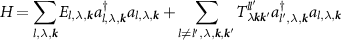
Standard image High-resolution imageTo evaluate this complex pump-probe signal we start by extracting the time-dependent population of different regions in momentum space that are indicated by colored boxes in figure 1(b). The population dynamics of the graphene  -band above and below the Fermi level is shown in figure 2(a) together with single-exponential fits (see SM). We find that gain and loss are asymmetric with lifetimes of
  ps and
  ps, respectively. The gain of photoelectrons above the equilibrium position of the WS2 valence band (figure 2(b)) shows an exponential lifetime of
  ps. The lifetime of photoexcited electrons at the bottom of the WS2 conduction band (figure 2(c)) is found to be
  ps.
ps.
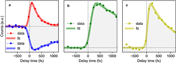
Figure 2. Population dynamics in different areas of momentum space. The data points in this figure were obtained by integrating the photocurrent over the areas marked by the colored boxes in figure 1(b). The color of the data points matches the color of the corresponding box. Continuous thick lines are exponential fits to the data. (a) Transient population of the Dirac cone of graphene above (red) and below (blue) the Fermi level. (b) Gain signal above the equilibrium position of the WS2 valence band. (c) Transient population of the WS2 conduction band.
Download figure:
Standard image High-resolution imageNext, we search for possible changes of the transient band structure by determining the binding energies for the WS2 valence and conduction band and the graphene Dirac cone as a function of pump-probe delay. To this end, we extract energy and momentum distribution curves (EDCs and MDCs), respectively, along the colored lines in figure 1(a) that we fit with an appropriate number of Gaussian (for EDCs) or Lorentzian peaks (for MDCs, see SM). The transient binding energies of the WS2 valence and conduction band are shown in figure 3(a). Subtracting the valence band position from the conduction band position yields the transient band gap shown in figure 3(b) together with a single-exponential fit. We find that the band gap decreases from the equilibrium value of  eV [15] to
  eV at
eV at  fs with a lifetime of
  ps. Assuming that the band gap shrinks symmetrically about its center, we can subtract the contribution of the transient band gap renormalization from the transient peak positions in figure 2(a). This yields the data in figure 2(c) where both the WS2 valence and conduction band show a remaining up-shift of
  meV with an exponential lifetime of
  ps. In figure 3(d) we plot the transient position of the Dirac cone that we obtain by multiplying the transient position of the MDC peak with the slope of the Dirac cone. We find that the Dirac cone shifts down by
  meV with a lifetime of
  ps.
ps.
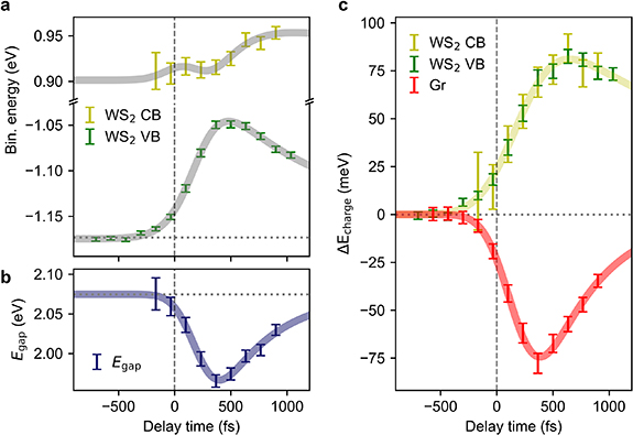
Figure 3. Transient band structure of WS2-graphene heterostructure. (a) Transient positions of WS2 valence (green) and conduction band (gold) at the K-point of WS2. Thick grey lines are calculated from the exponential fits in (b) and (c). (b) Transient band gap of WS2 together with exponential fit (thick line). (c) Band shifts due to charge separation of WS2 (green and gold) and graphene (red) together with exponential fit (thick lines).
Download figure:
Standard image High-resolution imageIn summary, we find that (i) the population dynamics in graphene are highly asymmetric with a short-lived gain and a long-lived loss, (ii) there is a strong gain of photoelectrons above the equilibrium position of the WS2 valence band with a lifetime of  ps, (iii) the transient band gap of WS2 reduces by
  % with a lifetime of
  ps, (iv) after subtracting the contribution of the transient band gap renormalization, all WS2 states show a remaining upshift of
  meV with a lifetime of
  ps, and (v) the Dirac cone shifts down by
  meV with a lifetime of
  ps.
ps.
4. Discussion
The experimental results in figures 1–3 are in good agreement with previous trARPES data supporting the previous interpretation in terms of a transient charge separated state [13, 15]. There, photoexcitation of the A-exciton in WS2 is followed by efficient charge transfer of both electrons and holes into the graphene layer. The fact that hole transfer is considerably faster than electron transfer then results in the formation of a charge-separated transient state with a lifetime on the order of  ps. The transient charge separation with electrons located in the conduction band of WS2 and holes located in the valence band of graphene explains the asymmetric population dynamics of the Dirac cone in figure 2(a) as well as the band shifts in figures 3(c) and (d). The gain of photoelectrons above the equilibrium position of the WS2 valence band contains contributions of both the transient band gap renormalization and the transient charge separation.
The obvious driving force for ultrafast charge transfer in vdW heterostrustures is the band alignment and the fact that photoexcited electrons and holes tend to relax to the CBM and VBM of the heterostructure, respectively. For type I band alignment (see figure 4(a)) both the CBM and VBM are located in the same layer. Provided that the other layer is photoexcited, both electrons and holes are expected to change layer during relaxation. For type II band alignment (see figure 4(b)) the CBM and VBM are located in different layers such that either electron or hole transfer is expected [7, 32].
Figure 4. Influence of band alignment on ultrafast charge transfer. (a) Type I band alignment: resonant excitation of the layer with the bigger band gap (red) results in charge transfer of both electrons and holes into the layer with the smaller band gap (blue). The transfer rates for electrons and holes are, in general, not the same. (b) Type II band alignment: photoexcitation of the red layer results in electron transfer into the blue layer. Similarly, excitation of the blue layer would result in hole transfer into the red layer.
Download figure:
Standard image High-resolution imageInitially, it seemed surprising that charge transfer can occur on ultrafast femtosecond to picosecond time scales despite the weak vdW coupling between the layers. This issue was resolved by envoking a coherent transfer channel allowing electrons and holes to oscillate back and forth between the layers with frequencies on the order of  Hz [17, 33, 34]. This coherent oscillation is made possible by momentum-dependent orbital hybridization resulting in wave functions that are delocalized over both participating layers [34, 35]. Electrons and holes then transfer into the neighboring layer at constant energy, requiring energy dissipation into phonons to prevent back-transfer and to allow for carrier relaxation into the CBM or VBM [17, 33–36].
At this level, this phonon-assisted coherent charge transfer model is quite general. It becomes material specific for several reasons: (1) the locations of CBM and VBM obviously depend on the band structures of the individual layers and their relative alignment in the heterostructure. (2) Charge transfer relies on orbital hybridization between the individual layers that sensitively depends on interlayer distance and twist angle. (3) Charge transfer rates depend on the size of the respective tunneling matrix element, the available phase space, the electron-phonon coupling strength, and the phonon frequencies.
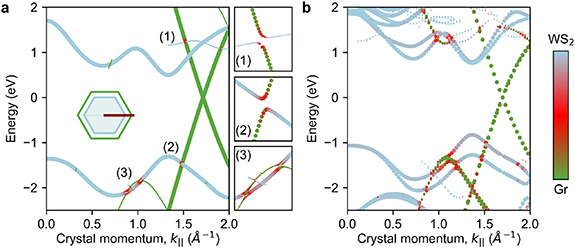
In order to apply this model to our WS2-graphene heterostructure we start by calculating the band structure of the heterostructure within the tight-binding approximation and using DFT. The unfolded hybrid band structures are shown in figure 5. The bands are color-coded to illustrate the degree of hybridization. The size of the data points is linked to the probability of finding an electron in that particular state. Overall, the two theories provide very similar results. Minor differences in the k-space region around  in the lowest conduction band are attributed to the comparative simplicity of the tight binding description. The heterostructure exhibits type I band alignment with both the CBM and the VBM located inside the graphene layer. Hence, both electrons and holes originally generated by excitonic absorption inside the WS2 layer are expected to transfer into the graphene layer. Charge transfer is expected to occur in those regions of the Brillouin zone where the wave function is delocalized over both layers. Our calculations reveal several avoided crossings with delocalized wave functions (red in figure 5) both in the conduction and the valence band of the heterostructure.
Figure 5. Band structure calculations for WS2-graphene heterostructure with a twist angle of  . (a) Tight-binding model. (b) DFT calculations. The size of the data points indicates the probability of finding an electron in that particular state. The color code indicates the orbital composition of the wave function.
Download figure:
Standard image High-resolution image
Photoexcitation at resonance to the A-exciton of WS2 initially places electrons and holes at the CBM and VBM at the K-point of the WS2 layer where the graphene contribution to the wave function is negligible. In order to transfer into the graphene layer both electrons and holes need to reach the closest avoided crossing in the band structure of the heterostructure. In figure 5(b) we see that, for electrons, the closest charge transfer state is located around  , separated from the CBM by an energy barrier of
  meV. For holes, we find
  and
and  meV. Overcoming these barriers requires excess kinetic energy which explains the previously observed pump fluence dependence of the transfer rates [15]. According to time-dependent DFT and non-adiabatic molecular dynamics simulations in [17] the in-plane bond stretching E2g mode of graphene and the out-of-plane A1g mode of WS2 provide the required energy dissipation for charge transfer from WS2 to graphene.
To optimize charge transfer rates of a given heterostructure (i.e. a given combination of materials) for desired applications the phonon-assisted coherent charge transfer model described above suggests the following control parameters: (1) the twist angle between the layers will affect the hybridization between the layers with immediate impact on charge transfer states [37–39]. (2) The relative band alignment of the heterostructure can be controlled via perpendicular electric fields which yields control over the available phase space [17, 40, 41].
5. Conclusion
We combined trARPES measurements with tight binding and DFT band structure calculations to investigate the microscopic pathways for ultrafast charge separation and recombination in the heterostructure. Despite the weak vdW interaction between the layers we find indications for strong hybridization enabling ultrafast phonon-assisted coherent charge transfer. Based on these findings we propose to vary twist angle and band alignment to tailor electron and hole transfer rates for specific applications.
Acknowledgments
The research leading to these results has received funding from the Deutsche Forschungsgemeinschaft through CRC 1277 (Project 314695032) and CRC 1038 (Project 223848855), and the European Union's Horizon 2020 research and innovation program under Grant Agreement No. 851280-ERC-2019-STG and 881603-Graphene Core3.
Data availability statement
The data cannot be made publicly available upon publication because the cost of preparing, depositing and hosting the data would be prohibitive within the terms of this research project. The data that support the findings of this study are available upon reasonable request from the authors.
Supplementary data (3.4 MB PDF)