
Abstract
Layered materials (LMs) produced by liquid phase exfoliation (LPE) can be used as building blocks for optoelectronic applications. However, when compared with mechanically exfoliated flakes, or films prepared by chemical vapor deposition (CVD), LPE-based printed optoelectronic devices are limited by mobility, defects and trap states. Here, we present a scalable fabrication technique combining CVD with LPE LMs to overcome such limitations. We use black phosphorus inks, inkjet-printed on graphene on Si/SiO2, patterned by inkjet printing based lithography, and source and drain electrodes printed with an Ag ink, to prepare photodetectors (PDs). These have an external responsivity (Rext)∼337 A W−1 at 488 nm, and operate from visible (∼488 nm) to short-wave infrared (∼2.7 µm, R 48 mA W−1). We also use this approach to fabricate flexible PDs on polyester fabric, one of the most common used in textiles, achieving R
 6 mA W−1 at 488 nm for an operating voltage of 1 V. Thus, our combination of scalable CVD and LPE techniques via inkjet printing is promising for wearable and flexible applications.
Export citation and abstract BibTeX RIS

Original content from this work may be used under the terms of the Creative Commons Attribution 4.0 license. Any further distribution of this work must maintain attribution to the author(s) and the title of the work, journal citation and DOI.
1. Introduction
1.1. Background
Photodetectors (PDs) are key components of video imaging [1], optical communications [2], night vision [3], gas sensing [4] and many other devices.
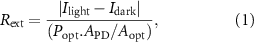
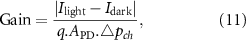
Their responsivity can be expressed as external [5, 6]:
or internal [6]:
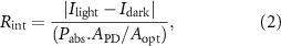
where Ilight and Idark are the currents of the PD under illumination and in dark conditions. APD and Aopt are the PD area and the laser spot size.  is a scaling factor that takes into account the fact that only a fraction of optical power impinges on the PD. Popt is the incident optical power, and Pabs =
  is the absorbed optical power, where 0
 1 is the optical absorption in the PD. Typically,
  1, since not all incident photons are absorbed (P
 ) [6], therefore R
 [6]. Rext describes the overall PD responsivity, including device-related considerations, such as PD design and architecture, light absorption and reabsorption (i.e. the absorption of radiatively recombined photons in the PD photoactive materials), optical reflection from interfaces, optical path in the photoactive area, materials quality, etc [6]. On the other hand, Rint provides an estimate of the photodetection efficiency, characterizing the optical-to-electrical conversion process of the absorbed photons [6]. Rext is related to Rint as [6]:
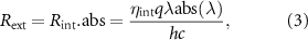
where ηint is the internal quantum efficiency, i.e. the ratio of the number of charge carriers collected from the photoactive layer to the number of absorbed photons [6], q is the electron charge, λ is the incident light wavelength, h is the Planck constant, and c the speed of light.  is wavelength dependent, therefore the spectral response in quantum-type PDs (whereby photons generate electron–hole, e-h, pairs) typically follows the absorption spectrum of the light-absorbing material [6].
The response time (τlife) is the lifetime of the photogenerated charges in the light-absorbing layer [5]. This determines the PD speed, defined as [5, 6]:
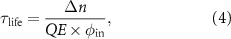
where  is the light-induced change in carrier density, QE is the external quantum efficiency, defined as QE =
  where ηtran is the charge transfer efficiency (i.e. the ratio between the flux of charges that contribute to the current and the total light flux that reaches the surface), ηabs is the light absorption efficiency (i.e. the percentage of light absorbed by the sample), and φin is the incoming photon flux. The operation wavelength range is the spectral range where the PD is sensitive to incident light [6]. For cameras and video imaging, detection in the visible (∼400–700 nm) with
  10–50 ms is desired [5]. R
 0.1 A W−1 can remove the need of amplifiers (to increase the output with respect to the input signal (i.e. current)) [7], thus decreasing costs [7].
PDs currently in the market are mainly based on Si complementary metal-oxide-semiconductor (CMOS) technology [8]. For applications in the short-wave infrared (SWIR) (1000–2500 nm/1.24–0.5 eV), beyond the Si bandgap (1.1 eV) [6], current technology relies on III-V InGaAs PDs [9]. However, these require complex manufacturing steps (epitaxial growth) [10], cooling to liquid nitrogen [10], and they are rigid [10].
1.2. Layered materials-based photodetectors
Graphene and related materials (GRMs) are promising for PDs [5, 11], and have demonstrated R
 108 A W−1 at 532 nm [12], with response time
  [13], 110 GHz speed [14], operation wavelength covering visible to the mid-IR ∼3.2 µm [15] and THz [16, 17], and CMOS integrability [18]. Many GRM-based PDs fabricated based on scalable chemical vapor deposition (CVD) approaches [19, 20] were also reported, with R
 121 A W−1 at 532 nm [20]. R
 A W−1 was achieved integrating graphene flakes [12] and/or layered materials (LMs), such as MoS2, [21] with PbS [22, 23] and HgTe quantum dots (QDs) [24], with spectral coverage determined by the absorption of the added material (e.g. QDs) [22].
In graphene-based PDs (e.g. metal-graphene-metal PDs [25]),  is governed by the wavelength dependent optical conductivity of SLG [26], doping [26], Pauli blocking [26], mobility [27], scattering time [28], device architecture, and substrate, which affects the optical path and the interference of the incident light [25]. In graphene PDs based on photogating (e.g. graphene/QDs [12], graphene/semiconductor [29]), abs(λ) depends on the absorption coefficient profile (4πK/λ) [6] of the light-absorbing material, where K is the imaginary part of the photoactive material [6].
Liquid phase exfoliation (LPE) is a promising route for production of LM-based inks [30–35]. These have been used for printed solar cells [36], sensors [37], transistors [32], supercapacitors [38, 39], and PDs [40]. LPE inks were used to prepare PDs on rigid (e.g. Si) [41] and flexible (e.g. PET(polyethylene terephthalate)) [42] substrates. Challenges in the development of inkjet-printed LPE based PDs stem from the limitations associated with the presence of traps (surface [43, 44] and interface sites [43, 44] formed during LPE), resulting in photocurrent loss [44].
PDs based on solution-synthesized MoS2 on Si/SiO2 were demonstrated [44]. These were prepared by dissolving (NH4)2MoS4 in dimethylformamide:butylamine:aminoethanol (volumetric ratio of 4.5:4.5:1), followed by spin coating on Si/SiO2 and conversion to MoS2 via annealing at 750 ∘C and 1000 ∘C under Ar/H2 and Ar/S [44]. The MoS2 channel was defined by photolithography (PHL) and dry etching using O2 plasma. The electrodes were fabricated via e-beam evaporation of Au/Ti. However, the PDs in reference [44] showed R limited to ∼63 µ A W−1 at 405 nm [44], due to the presence of defects [44]. These acted as trap states and resulted in a slow (few s) τlife. The current (∼10−9A when the light was turned on) did not recover to the initial level (∼3×10⁻¹²A with light off [44]). τlife improved to ∼20 ms by applying a gate pulse ∼100 V to discharge the trapped charges [44]. Lateral heterostructures based on LPE MoS2 flakes as photoactive material and ∼4 layer graphene (4LG) flakes [40, 45] or Ag paste [46] as electrodes were reported [40, 45, 46], with R
 36 µ A W−1 and
  60 ms at 532 nm [46], and 300 mA W−1 under white light. Reference [47] reported LPE MoS2 based PDs with R
 50 mA W−1 at 515 nm and
  5 ms, using ethyl cellulose to make percolating films with conductivity ∼1.72×10⁻²S m−1 [47]. Water-based
  7LG and WS2 inks were used in reference [42] to make vertical heterostructures, resulting in PD arrays. However, these PDs mostly cover visible (405–532 nm) [40, 42, 44–47] with R
 50 mA W−1, due to photocurrent loss mainly due to traps [43, 44].
Black phosphorus (BP) is a LM interesting for broad-band PDs because of its thickness dependent direct bandgap varying from ∼0.3 eV in bulk [48] to ∼2 eV in 1LBP [49]. Micro-mechanical cleavage (MC) has been the main approach used to make BP PDs [50–57]. Reference [56] demonstrated PDs based on BP flakes with thickness ∼10 nm [56], working from ∼532 to 3390 nm, with R 82A W−1 at 3.39
  and
and  0.13 ms. BP was exfoliated on Si/SiO2. A resist layer was patterned via e-beam lithography (EBL) for metallization and evaporation of Cr/Au as contacts [56]. Reference [53] used MC BP (∼8 nm thickness), EBL, and electron-beam evaporation to form arrays of metal contacts. Reference [53] demonstrated BP-based PDs for 400–900 nm, with R
 106A W−1 at 400 nm, ∼103 A W−1 at 900 nm and
  5 ms. Reference [50] used a 225 nm thick BP film stacked between two SLGs as top and bottom contacts. To prevent exposure to the environment, this was encapsulated in 18 nm hBN [50]. The PDs had broadband response ∼632–3400 nm, with R
 0.15 A W−1 at 632 nm, ∼1.43 A W−1 at 3400 nm, and
  1.68 ns [50]. However, MC usually produces flakes
  1 mm [58], without thickness control (random locations of 1L to tens nm flakes) [59, 60], and lacks reproducibility in terms of amount of material, flake size, and number of layers [61–65]. Reference [41] used LPE BP inks to print BP/CVD SLG/Si Schottky junction PDs, with R
 164 mA W−1 at 450 nm, ∼1.8 mA W−1 at 1550 nm, and
  0.55 ms [41]. Si/SiO2 was patterned with EBL, followed by e-beam evaporation of Au and lift-off. The devices were further patterned to make a window to etch SiO2. CVD SLG was then transferred, covering the Au electrode and the Si window [41]. BP was inkjet-printed on the SLG/Si Schottky junction. This process is complex and requires expensive fabrication tools (EBL and e-beam evaporator). Reference [66] reported SLG/LPE BP PDs. Two Au electrodes were evaporated through a shadow mask on Si/SiO2. CVD SLG was wet transferred on the printed LPE BP. The resulting SLG/BP film was transferred on Si/SiO2 with Au electrodes [66]. These PDs had R
 103 A W−1 at 360 nm at 5 V bias, with
  7 s and operation wavelength ∼360–785 nm [66]. Table 1 compares the results of MC BP and inkjet-printed BP PDs with different device structures [41, 42, 44–47, 50, 52, 53, 56, 67–71, 182–185]. To the best of our knowledge, there are no reports of inkjet-printed PDs with broadband operation from visible (∼400–700 nm) to SWIR (∼2500 nm), with R
 1 A W−1 in visible and
  10–50 m, suitable for video imaging [72].
Table 1. PDs based on MC BP and LPE BP. IP (inkjet printing), EBL , PHL, UVL (UV lithography). t: average LM film thickness.
| Properties | ||||||
|---|---|---|---|---|---|---|
| Fabrication | Spectral range (nm) | Rext(A W−1) | Response time (s) | NEP ( ) ) | D (Jones) (Jones) | References |
| IP (LPE BP t∼200 nm) | 488–2700 | 337–0.048 (488–2700 nm) | 50 × 10−3 | 1.68 × 10⁻¹⁰ | 1011 | this work |
| IP (LPE MoS2 t∼1.9 µm) | white light | 0.3 | – | – | 3.6 × 10¹⁰ | [45] |
| IP (LPE MoS2 t∼700 nm) | 515 | 0.05 (515 nm) | 5×10⁻³ | – | 3.2 × 10⁹ | [47] |
| IP (LPE MoS2 t∼1.3 mm) | 405–980 | 63 (520 nm) (520 nm) | 20 × 10−3 | – | 4.2×10⁸ | [44] |
| IP (LPE MoS2 t∼50 nm) | 532 | 36 (532 nm) (532 nm) | 60×10−3 | – | – | [46] |
| IP (LPE WS2 t∼100 nm) | 514 | 0.001(514 nm) | – | – | – | [42] |
| IP (CVD MoS2 t=1L) | 405–780 | 0.02–0.01 (405–780 nm) | 1.7 | – | 4.8 × 10⁷ | [69] |
| IP (LPE WS2 t∼30 nm)/PHL | 632 | 10−4(632 nm) | – | – | – | [70] |
| IP (LPE BP)/EBL | 450–1550 | 0.164(450 nm) | 550 × 10−6 | – | – | [41] |
| EBL (MC BP t∼8 nm) | 640–940 | 4.8 × 10⁻³ (640 nm) | 4 × 10⁻³ | – | – | [52] |
| EBL (MC BP t∼10 nm) | 532–3390 | 82 (3390 nm) | 130 × 10−6 | 5.6 × 10⁻¹² | – | [56] |
| EBL (MC BP t∼10 nm) | 830 | 53(830 nm) | – | – | – | [71] |
| EBL (MC BP t∼30 nm) | 400–3750 | 0.35 × 10⁻³(1200 nm) | 40 × 10−6 | – | – | [67] |
| UVL (MC BP t∼60 nm) | 635–1550 | 594–3300(635–1550 nm) | 3 × 10⁻³ | – | – | [68] |
| EBL (MC BP t∼8 nm) | 400–900 | 4.3 × 10⁶–103(400–900 nm) | 5 × 10⁻³ | – | – | [53] |
| EBL (MC BP t∼225 nm) | 632–3400 | 0.15–1.43(632–3400nm) | 1.8 × 10⁻⁹ | 7×10⁻¹² | – | [50] |
| Abration (WS2 t∼30 nm) | 625 | 144 (625 nm) (625 nm) | 70 × 10−6 | – | 108 | [181] |
| Sputtered (WS2 t∼4 nm) | 450–635 | 1.68 (450 nm) (450 nm) | – | – | – | [182] |
| EBL (WS2 t∼7.2 nm) | 405–635 | 160 (405 nm) (405 nm) | 21×10−3 | – | 1.4 ×10¹¹ | [183] |
| MLL (Carbon QDs/MoS2 t=1L) | 300–700 | 377(360 nm) | 7.5 | – | 1.6 × 10¹³ | [184] |
| Abration (MoS2 t=15–25 µm) | 365–940 | 1.5 × 10⁻⁶(660 nm) | 20–30 | – | – | [185] |
Printing can be used for large-scale( 1 m2) [73] fabrication of optoelectronic devices on both rigid [74] and flexible [75] substrates. A variety of printed devices have been reported [76], such as radio-frequency identification tags on paper [77, 78], sensors [79], displays [80], memories [81], and thin-film transistors [32]. Printing was performed with different methods, such as screen [82, 83], gravure [84], flexography [85], and inkjet [32, 86]. Amongst those, inkjet printing is one of the most promising, because of attractive features such as direct patterning (mask-free) [87, 88] and resolution [89, 90]. The typical printing resolution is ∼100 µm for gravure [91], ∼100–200 µm for flexo [91], ∼100 µm for screen printing [91]. Inkjet printing offers resolution down to ∼50 µm [92], which can be made
 500 nm by pre-patterning [93]. Inkjet printers can also be used to dispense etching [94] or patterning agents [95].
Here we use inkjet printing to fabricate SLG/BP PDs. CVD SLG is patterned by inkjet printing polyvinylpyrrolidone (PVP) as mask, followed via reactive ion etching (RIE). PVP is rinsed with water. Source-drain Ag electrodes are then inkjet-printed at the end of the SLG channel. LPE BP is inkjet-printed on the channel, followed by encapsulation using Parylene C to prevent BP oxidation [96].
Our PDs have Rext up to ∼337 A W−1 at 488 nm for 1 V bias, the highest reported to date for inkjet-printed LPE LMs, to the best of our knowledge, see table 1. Our PDs work in the range ∼488 nm−2.7 µm, the broadest for inkjet-printed based PDs, to the best of our knowledge, see table 1. Instead of TMDs, which have tuneable indirect band gap in bulk crystals [97] and direct band gap in 1L [98], we use BP, which exhibits thickness dependent direct bandgap from ∼0.3 eV in bulk [48] to ∼2 eV in 1L [49]. R is proportional to the mobility, µ, as [6]:
with τlife the response time, V
 the bias applied between source and drain, and L the channel length. The term
  is called gain [6]. By increasing µ, the gain increases, which results in higher Rext. Therefore, we use CVD SLG with
  1700 cm2 V−1s−1, instead of solution-processed graphene with
  300 cm2 V−1s−1 as in reference [99].
To demonstrate the viability of our approach for flexible and wearable electronics, we fabricate SLG/BP PDs on polyester fabric, with R
 6 mA W−1 at 1 V and 488 nm, higher than CVD SLG PDs (R
 0.11 mA W−1) on flexible (acrylic) substrates [100], and comparable to CVD MoS2 PDs (R
 20 mA W−1 at 405 nm) with inkjet-printed poly(3,4-ethylenedioxythiophene) polystyrene sulfonate (PEDOT:PSS) on polyethylene naphthalate (PEN) [69], but with surface roughness lower than our fabric. Thus, inkjet lithography is promising for LMs-based optoelectronic devices on textiles.
2. Results
2.1. Inkjet printing
BP bulk crystals are sourced from Smart-elements GmbH. These are then exfoliated as follows. 15 mg are transferred to a mortar and ground for ∼20 min to facilitate subsequent sonication. BP powders are then mixed with 15ml anhydrous isopropyl alcohol (IPA) (Sigma-Aldrich) in a Schlenk flask, sealed with parafilm, and sonicated for 3 h in a 900 W ultrasonic bath (Fisherbrand Elmasonic S 300 Ultrasonic). The BP solution is then centrifuged (H-641 swinging bucket rotor in a Sorvall WX-100) at 4000 rpm (∼6000 g) for 20 min to let the unexfoliated flakes sediment [64, 101]. The supernatant is collected and used for characterization and printing. All procedures are carried out in a glove box (inert atmosphere to minimise BP exposure to the environment or air), except the centrifugation.
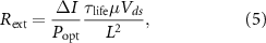
The BP crystals are characterized by Raman spectroscopy using a LabRAM HR Evolution equipped with a 100× objective with power on the sample  0.5 mW, to exclude heating effects, figure 1. Bulk BP (red) has three main peaks, figure 1(b). One out-of-plane A
 mode, with position Pos(A
 ) ∼362.6 cm−1 [60, 96, 102–104] and two in-plane B
 and A
and A modes, Pos(B
 ) ∼439.5 and Pos(A
 ) ∼467.1 cm−1 [60, 96, 102–104]. The corresponding full width at half maximum (FWHM) are FWHM(A
 ) ∼2 cm−1, FWHM(B
 ) ∼3.5 cm−1, FWHM(A
 ) ∼2.5 cm−1. The peaks ∼194 and ∼230 cm−1 are assigned to B
 and B
and B modes [105]. These are expected to appear when the incident light has a polarization component along the axis orthogonal to the BP layers [106]. However, we detect both, although we are in backscattering, as for previous reports [105–107].
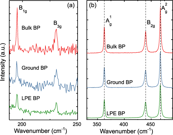
Figure 1. (a), (b) Raman spectra measured at 514.5 nm of (red) BP bulk crystals, (blue) ground BP, (green) LPE BP.
Download figure:
Standard image High-resolution imageThe ground BP sample (blue curve in figure 1) has Pos(A ) ∼362.6 cm−1, FWHM(A
 ) ∼2.1 cm−1, Pos(B
 ) ∼439.4 cm−1, FWHM(B
 ) ∼3.8 cm−1, Pos(A
 ) ∼466.9 cm−1 with FWHM(A
 ) ∼2.7 cm−1, figure 1(b). We observe
  0.3 cm−1 change in FWHM and Pos(A
 , B
, B , A
, A ) compared to bulk BP, indicating the presence of flakes with number of layers, N
 6 [96].
The LPE BP flakes (green in figure 1) have Pos(A ) ∼362.6 cm−1, FWHM(A
 ) ∼2.3 cm−1, Pos(B
 ) ∼439.3 cm−1, FWHM(B
 ) ∼3.9 cm−1, Pos(A
 ) ∼466.9 cm−1, FWHM(A
 ) ∼2.8 cm−1, figure 1(b). We observe
  0.5 cm−1 change in FWHM and Pos(A
 , B
, B , A
, A ) compared to bulk BP, indicating N
 6 [96].
Stable jetting happens when a single droplet is produced for each electrical impulse, with no secondary droplet formation [92]. This depends on ink viscosity η (mPas) [108], surface tension γ (mNm−1) [108], density ρ(gcm−3) [108] and nozzle diameter D ( ) [109]. A dimensionless figure of merit (FOM)
  was suggested to characterize the stability of inkjetting [108, 109]. [110] reported that if
  the ink would not jet,
  would result in secondary droplets. Therefore,
  is generally considered as the optimal range for stable drop-on-demand [108, 109]. However, we previously showed that drop-on-demand inkjet printing of LM inks with
  is possible [32]. By changing η, γ, and ρ, we are able to tune Z across and outside the conventionally optimal range, and modify our inks for drop-on-demand printing. The size of flakes in solution should be
  smaller than the nozzle diameter to prevent clogging [32], and clustering of the particles at nozzle edge [32]. Flakes tend to concentrate at the droplet edge during evaporation, resulting in a ring-like deposit, the so-called coffee-ring effect [111], leading to printing non-uniformity [111]. Adding polymer binders into the LPE dispersion [39, 46, 112] might prevent [39] or alleviate [39] the formation of coffee-rings [39, 46, 112]. However, binders decrease electrical conductivity [39], and must be annealed for removal (e.g. baking on a hot plate at 300 ∘C–400 ∘C for ∼1 h [39]). Solvents like N-Methyl-2-pyrrolidone (NMP) are generally the preferred option to disperse BP because of NMP's surface tension and Hansen solubility parameters [31, 113]. However, a temperature close to the NMP boiling point (204 ∘C) [114]) is required to remove NMP residuals [91], but this can cause oxidation [64, 96] and degradation [64, 96] of air-sensitive BP [41]. NMP is also toxic [115] and can affect the central nervous system [116], so LMs inks dispersed in NMP cannot be used in an open environment [39]. Therefore, it is better to formulate BP inks in nontoxic solvents, with boiling point
 C.
C.
We prepare our BP ink in anhydrous IPA (not as toxic as NMP [121], and commercially available as a 70 solution in rubbing alcohol and hand sanitizers [121]), with a boiling point ∼83 ∘C [114]. The surface tension and viscosity are characterized via contact angle, surface tension (First Ten Angstroms) and rheometery (Discovery HR-1) measurements at room temperature (RT) and ambient pressure. The BP ink has
  0.55 mPas,
  26 mNm−1 and
  0.8 gcm−3. For printing we use a Fujifilm Dimatix DMP-2800 with D = 22 µm, resulting in Z = 35, outside the conventional optimal range [110]. We aim for BP flake sizes∼1 µm to prevent nozzle clogging [32]. Scanning tunneling electron microscopy (STEM) (Magellan 400 L) is used to measure the flakes lateral size.
Figures 2(a) and (b) are a representative STEM image and a statistical analysis on 140 flakes, indicating mean length ∼220 nm and mean width ∼96 nm. The thickness distribution is estimated by Atomic Force Microscopy (AFM, Bruker Dimension Icon). Figure 3(a) is a typical AFM image of one flake, with thickness ∼5.4 nm, figure 3(b), corresponding to N ∼11. The AFM statistics on 140 flakes shows an average thickness ∼6.7 nm, figure 3(c), corresponding to N ∼13, given a 1 L-BP thickness ∼0.5 nm [122].
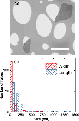
Figure 2. (a) Representative STEM image of LPE BP. Scale bar 1 µm. (b) Size statistics of 140 flakes.
Download figure:
Standard image High-resolution image
Figure 3. (a) Representative AFM image of BP flake, and (b) height profile. (c) AFM thickness statistics of 140 flakes.
Download figure:
Standard image High-resolution imageFigure 4(a) plots the absorbance, Abs = −log10(Tr) [123], with Tr the transmittance of the BP ink measured with a Cary 7000 UV–VIS–NIR Spectrometer. The BP concentration is estimated from the Beer–Lambert Law [124, 125] Abs =  , where c [gL−1] is the concentration,
  ext
[Lg−1m−1] the extinction coefficient, and l[m] is the cuvette length [126]. Reference [64] experimentally derived the BP ext
at 660 nm from the slope of Abs per length versus the concentration of BP,
ext
[Lg−1m−1] the extinction coefficient, and l[m] is the cuvette length [126]. Reference [64] experimentally derived the BP ext
at 660 nm from the slope of Abs per length versus the concentration of BP,  267 Lg−1m−1, with c calculated by measuring the weight difference of the collected BP flakes on an anodic aluminum oxide membrane before and after vacuum filtration [64]. From this, we estimate c ∼0.36 gL−1 for our ink, similar to reference [64].

Figure 4. (a) Absorbance of LPE BP. The ambient moisture absorbed by the IPA results in absorbance variations at ∼1700–1800 nm [41]. The dispersions are diluted 6 times to avoid detector saturation. (b) HRTEM image of representative BP flake, scale bar 10 nm. (c) Zoom of (b), scale bar 5 nm. The crystal plane spacing is ∼0.21 nm, corresponding to the (002) plane of orthorhombic phosphorus [117]. (d) Representative XPS of LPE BP flake, showing the  and
and  129.7 [64, 118] and 130.5 eV [64, 118]. Small POx
sub-bands are seen ∼134 eV [118–120].
129.7 [64, 118] and 130.5 eV [64, 118]. Small POx
sub-bands are seen ∼134 eV [118–120].
Download figure:
Standard image High-resolution imageHigh-resolution transmission electron microscopy (HRTEM) images are obtained via a FEI Tecnai F20 FEG TEM operated at 200 keV on BP flakes transferred on holey carbon grids. Figures 4(b) and (c) indicate a crystal plane spacing ∼0.21 nm, corresponding to the (002) plane of orthorhombic phosphorus [117], with N ∼15, and overall thickness ∼7.5 nm, consistent with the flake distribution range obtained by AFM in figure 3(c).
X-ray photoelectron spectroscopy (XPS) (Thermo Fisher ESCALAB 250Xi) is then performed to assess the chemical composition of the BP flakes. The samples for XPS are prepared in an Ar glove box by drop-casting the BP dispersion onto Si/SiO2, followed by N2 gas flushing on a hot plate (60 ∘C) for ∼5 min. Figure 4(d) shows the  and
and  spin-orbit split doublet ∼129.7 [64, 118] and ∼130.5 eV [64, 118], consistent with previous XPS measurements on bulk BP [119, 127]. The sub-bands ∼134 eV are attributed to surface suboxides introduced during LPE, as for [64, 118].
2.2. SLG/BP on Si/SiO2
The design of our SLG/BP PD is shown in figure 5(a). SLG is the channel on Si/SiO2, Si is the bottom gate, SiO2 is the dielectric, BP is the photoactive material, Ag is used for the electrodes, and Parylene C as encapsulation layer. Upon illumination, electron–hole (e-h) pairs are photogenerated in BP. Due to the band alignment (figure 5(b)) h are transferred from the BP valence band (VB) into SLG, leaving behind uncompensated e, acting as an additional negative gate bias, leading to a photogating effect [12]. A schematic band diagram of the SLG/BP interface is in figure 5(b). A built-in field is formed at the SLG/BP interface. Upon BP photoexcitation, h are transferred to SLG under the built-in field, leaving e trapped in BP. Figure 5(c) is a false color SEM image of the SLG/BP PD.
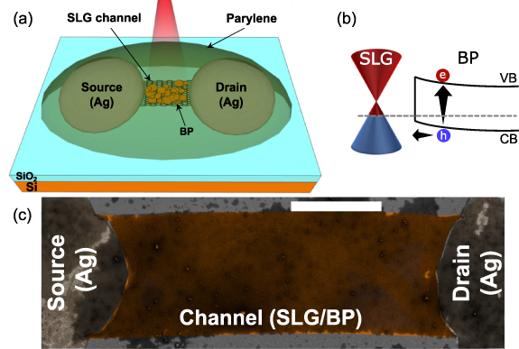
Figure 5. (a) Schematic of SLG/BP PD. SLG is the channel (black honeycomb), BP is the photoactive material (orange), Ag is used for electrodes (silver), Parylene C as encapsulation layer (transparent green), incident light (red). (b) Schematic band diagram of SLG/BP interface, showing the BP CB and VB, generation of e/h pairs and transfer of h from BP to SLG. (c) False colour SEM image of SLG/BP PD on Si/SiO2. BP is inkjet-printed on SLG channel (orange). Ag inkjet-printed source and drains are shown in silver. Scale bar 15 µm.
Download figure:
Standard image High-resolution imageTo fabricate the SLG/BP PD, SLG is grown on a 35  Cu foil, as for reference [128]. The substrate is annealed at 1000 ∘C for 30min in the presence of 20sccm H2. To initiate growth, 5sccm CH4 is added. After growth, the sample is cooled to RT at 1mTorr.
The SLG quality is monitored at each step of the fabrication process by Raman spectroscopy. The Raman Spectrum of as grown SLG on Cu is in figure 6, after Cu photoluminescence (PL) removal [129]. The 2D peak is a single Lorentzian with FWHM(2D) ∼29 cm−1, signature of SLG [130]. Pos(G) is ∼1586 cm−1, with FWHM(G) ∼14 cm−1. Pos(2D) is ∼2703 cm−1, I(2D)/I(G) and A(2D)/A(G) are ∼3.1 and ∼6.4. No D peak is observed, indicating negligible defects [131].

Figure 6. Raman spectra at 514.5 nm of SLG on Cu (red), after transfer (gray), after patterning and PVP removal (purple), and after BP deposition with encapsulation of parylene C and subtraction of the parylene C signal (green). Spectra normalized to have the same I(G).
Download figure:
Standard image High-resolution imageThe fabrication process flow for SLG/BP PD is outlined in figure 7. To transfer SLG, poly(methyl methacrylate) (PMMA) is spin coated on SLG/Cu, followed by oxygen etching of SLG on the Cu backside, using a RIE-NanoEtch (3 W 30 s). Cu/SLG/PMMA is then left in ammonium persulfate (APS) in DI water for ∼6 h until Cu is etched. The resulting SLG/PMMA membrane is placed in DI water to clean the APS residuals and then transferred onto Si+90 nm SiO2, followed by overnight drying and PMMA removal with acetone and IPA, figure 7(a).
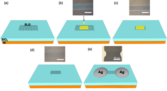
Figure 7. Inkjet lithography of SLG-FET. (a) CVD SLG is transferred on Si/SiO2, followed by overnight drying and PMMA removal using acetone/IPA. (b) PVP (yellow) is inkjet-printed on SLG. The optical microscopy image shows inkjet-printed PVP as mask on SLG. (c) SLG is then etched via RIE. The image shows the PVP ink on SLG after RIE etching. (d) PVP is removed by rinsing with water. The image shows patterned SLG after removal of PVP ink with water. (e) Ag ink (silver) is printed to make source and drain electrodes. The sample is placed on a hot plate at ∼150 ∘C for ∼2 h. The image shows the inkjet-printed Ag ink after ∼2 h annealing. Scale bars: 20 µm.
Download figure:
Standard image High-resolution imageThe Raman spectrum of SLG transferred on Si/SiO2 is in figure 6. The 2D peak retains its single-Lorentzian line shape with FWHM(2D) ∼31.6 cm−1. Pos(G)∼1594 cm−1, FWHM(G)∼11.6 cm−1 and Pos(2D)∼2693.1 cm−1, I(2D)/I(G) and A(2D)/A(G) are ∼1.2 and 3.2, indicating a p-doping with Fermi energy, E 450 meV [132, 133], which corresponds to a carrier concentration ∼12.3×1012cm−2 [132]. I(D)/I(G)∼0.06 corresponds to a defect density of ∼3.54 × 1010cm−2 [134, 135] for excitation energy 2.41 eV and E
 450 meV.
Pos(G) and Pos(2D) are also affected by the presence of strain. For uniaxial(biaxial) strain, Pos(G) shifts by ΔPos(G)/Δ  23(60) cm−1/
 [136, 137]. Pos(G) also depends on doping [132, 133]. The average doping as derived from A(2D)/A(G) should correspond to Pos(G)∼1599.2 cm−1 for unstrained SLG [132]. However, in our experiments Pos(G)∼1594 cm−1, which implies a contribution from uniaxial (biaxial) strain ∼0.22
 (0.08
(0.08 ) [136]. Local variations in strain and doping manifest as a spread in Pos(G) and Pos(2D), which in our sample vary from 1592 to 1597 cm−1 and from 2688 to 2696 cm−1, figure 8(a). In presence of uniaxial (biaxial) strain, and in the absence of doping, ΔPos(2D)/ΔPos(G)∼2.2 [136, 137]. In our samples ΔPos(2D)/ΔPos(G)∼0.87 (figure 8(a)), which indicates that most of the variation of Pos(G) is due to doping [136, 137]. This is also confirmed by the inverse correlation of FWHM(G) with Pos(G) in figure 8(d) [132, 138, 139].

Figure 8. Pos(2D) as a function of Pos(G) mapped across a 20 µm×20 µm region in SLG (a) after transfer, (b) after patterning and PVP removal, and (c) BP deposition. FWHM(G) as a function of Pos(G) mapped across a 20 µm × 20 µm region in SLG (d) after transfer, (e) after patterning and PVP removal, and (f) BP deposition.
Download figure:
Standard image High-resolution imageTo pattern the CVD SLG, we use an IPA based PVP ink as mask, to protect SLG during RIE etching. PVP is used due its solubility in IPA [140], stable jetting [92] and ease of removal with water [141]. To make the ink, 5mg PVP (Sigma-Aldrich) is dispersed in 5 ml IPA. The PVP ink has  1.25 mPas, as measured with Rheometery (Discovery HR-1),
  69 mNm−1, as determined with a FTA100 series contact angle and surface tension measurement system (First Ten Angstroms), and
  1 gcm−3, as derived by weighting a known volume of PVP ink via microbalance (Sartorius). For D = 22 µm, Z = 30. We use a Fujifilm Dimatix DMP-2800 to inkjet print PVP, while Si/SiO2 is kept at ∼60 ∘C to promote ink drying. To pattern SLG, PVP is printed on SLG to mask selected SLG regions, figure 7(b). Then, the sample is placed in a RIE to etch the uncovered SLG, figure 7(c). PVP is then removed by adding droplets of water, figure 7(d).
The Raman spectrum of etched SLG after PVP removal is in figure 6. The 2D peak retains its single-Lorentzian shape with FWHM(2D) ∼33.7 cm−1. Pos(G)∼1588.1 cm−1, FWHM(G)∼15.6 cm−1, Pos(2D)∼2689.6 cm−1, I(2D)/I(G) and A(2D)/A(G) are ∼1.7 and 3.8, indicating a p-doping with E 380 meV [132, 133], corresponding to a carrier concentration ∼8.7×1012cm−2 [132]. I(D)/I(G)∼0.08 corresponds to a defect density ∼4.3×1010cm−2 [134, 135] for excitation energy 2.41 eV and E
 380 meV, thus no significant additional defects are induced during inkjet-lithography. The doping estimated from A(2D)/A(G) should correspond to Pos(G)∼1596.4 cm−1 for unstrained graphene [132]. In our experiments Pos(G)∼1588.1 cm−1, which implies a contribution from uniaxial (biaxial) strain ∼0.36
 (0.13
(0.13 ) [136]. ΔPos(2D)/ΔPos(G)∼0.34 (figure 8(b)), which indicates that most of ΔPos(G) is due to doping [136, 137], as confirmed by the inverse correlation of FWHM(G) with Pos(G) in figure 8(e) [132, 138, 139].
Source and drain electrodes are then prepared by inkjet printing an Ag ink from Sigma-Aldrich (Ag dispersion, 736465), figure 7(e), with resistivity  cm, as measured via a Keithley source meter at the two ends of the channel layer. The linear relation between current and source-drain voltage, V
 , indicates an Ohmic contact between Ag and SLG channel, figure 9(a). The resistance of the channel is ∼2.07 kΩ. The average sheet resistance, RS
, of CVD SLG on Si/SiO2, measured using a 4-point probe method, is R
, indicates an Ohmic contact between Ag and SLG channel, figure 9(a). The resistance of the channel is ∼2.07 kΩ. The average sheet resistance, RS
, of CVD SLG on Si/SiO2, measured using a 4-point probe method, is R 600
600  . In SLG, RS
= (
. In SLG, RS
= ( )−1 [26], with
  the SLG conductivity. In SLG,
  =
=  [142] where n is the carrier density per unit area and q is the e charge. From n∼8.7 × 1012cm−2 derived from our Raman measurements, we get R
 450
450  , consistent with our RS
measurements.
, consistent with our RS
measurements.

Figure 9. (a) Current as a function of V
 . (b) Id
as a function of Vg
for V
. (b) Id
as a function of Vg
for V
 = 0.5 V. (c) Contact resistance of inkjet-printed Ag ink on CVD SLG. The dotted line is a fit to the data.
Download figure:
Standard image High-resolution imageWe then gate modulate the current between SLG source and drain. SLG shows ambipolar behavior with  1700 cm
 , figure 9(b), from [6]:
where  is the change in drain current,
  is the change in gate voltage, L is the channel length, W is the channel width, and Vds
is source-drain voltage. Cox
is the gate oxide capacitance =
is the change in gate voltage, L is the channel length, W is the channel width, and Vds
is source-drain voltage. Cox
is the gate oxide capacitance =  /t
/t , where
  F/cm is the vacuum permittivity,
  is the dielectric constant of SiO2 [6] and
  90 nm is the SiO2 thickness. We use 90 nm SiO2 in order to have a larger electric field at lower gate voltages. The SLG quantum capacitance (CQ
) can be calculated as [132, 143]:
90 nm is the SiO2 thickness. We use 90 nm SiO2 in order to have a larger electric field at lower gate voltages. The SLG quantum capacitance (CQ
) can be calculated as [132, 143]:
where  is the reduced Planck constant,
  is the SLG Fermi velocity [59, 144], pch
is the charge carrier concentration per unit area in the channel, and ni
is the intrinsic carrier concentration in SLG near the Dirac point induced by defects and impurities [143, 145–147]. From the Raman analysis we estimate
is the SLG Fermi velocity [59, 144], pch
is the charge carrier concentration per unit area in the channel, and ni
is the intrinsic carrier concentration in SLG near the Dirac point induced by defects and impurities [143, 145–147]. From the Raman analysis we estimate  8.7
8.7 . This gives
  . Thus, the total capacitance C
 = (1/C
 +1/C
+1/C C
C .
.
The contact resistance (Rc
) of the Ag printed ink on SLG is estimated from the transfer length method [6], making 6 Ag/SLG/Ag contacts at SLG channel lengths ∼60, 160, 175, 300, 305, 430 µm, figure 9(c). Rc
of the Ag printed ink on SLG is ∼11 K m (figure 9(c)). From the linear relation between current and voltage in figure 9(c), we derive an Ohmic contact between Ag and SLG for all 6 samples.
The BP ink is then printed to a thickness ∼200 nm to cover the whole SLG channel, as measured with a DektakXT Stylus Profilometer. To prevent BP oxidation and degradation during electrical and photodetection characterizations, the SLG/BP PD is sealed under vacuum using Parylene C dimers (Curtiss-Wright) with a parylene coater (SCS coating). This forms a barrier to moisture and gas permeability [148, 149]. References [41, 96] encapsulated BP flakes with parylene C to prevent BP degradation. Following encapsulation, our SLG/BP PDs are stable for  30 days under ambient conditions. Parylene dimers are vaporized at
  C. In a separate chamber, they are pyrolysed into monomers at
  C. The PD is held at RT, so that parylene polymerizes on contact with the surface, forming a conformal film [41].
The Raman spectra of SLG coated with BP and sealed with Parylene C are in figure 6, and, after subtraction of the parylene C signal, in figures 10(a)–(c). In the Raman spectrum of Parylene C, the peaks ∼1207, 1337, 1610 cm−1, figure 10(b), are attributed to CH in-plane vibrations [150, 151], CH2 wagging and twisting vibrations [150, 151], CH scissoring in CH2,and/or C-C skeletal in-plane vibrations of the aromatic rings [150, 151], respectively. The 2D peak retains its single-Lorentzian line shape, and narrows from FWHM(2D) ∼33.7 cm−1 to FWHM(2D)∼23.6 cm−1, figures 6 and 10(c). FWHM(G) narrows from ∼15.6 cm−1 to ∼9.2 cm−1, figures 6 and 10(b). FWHM(2D) and FWHM(G) narrow due to the homogeneous distribution of doping in SLG channel. Pos(G) is ∼1585.4 cm−1, Pos(2D)∼2684.8 cm−1, I(2D)/I(G) and A(2D)/A(G) are ∼2 and 5.3, indicating a n-doping with E 360meV [132, 133] which corresponds to carrier concentration ∼7.7×1012 cm−2 [132]. I(D)/I(G)∼0.25 corresponds to a defect density ∼13.0×1010 cm−2 [134, 135] for excitation energy 2.41 eV and E
 360 meV. EF
, as calculated from A(2D)/A(G), should correspond to Pos(G)∼1590.2 cm−1 for unstrained graphene [132]. We have Pos(G)∼1585.4 cm−1, which implies a contribution from uniaxial (biaxial) strain ∼0.21
360 meV. EF
, as calculated from A(2D)/A(G), should correspond to Pos(G)∼1590.2 cm−1 for unstrained graphene [132]. We have Pos(G)∼1585.4 cm−1, which implies a contribution from uniaxial (biaxial) strain ∼0.21 (0.08
(0.08 ) [136]. ΔPos(2D)/ΔPos(G)∼0.38 (figure 8(c)), which indicates that most of the variation of Pos(G) is due to doping [136, 137]. This is also confirmed by the inverse correlation of FWHM(G) with Pos(G) in figure 8(f) [132, 138, 139].

Figure 10. Raman spectra at 514.5 nm of parylene C (blue) on Si/SiO2 and SLG/BP sealed with parylene C (green) on Si/SiO2.
Download figure:
Standard image High-resolution imageSince device fabrication comprises many steps, monitoring the quality of graphene is essential, as it could affect µ. The Raman analysis provides information on doping, defects, and strain, which affect µ, thus Rext, as for equation (5). Both compressive and tensile strains can affect µ [152]. [152] reported that a change in strain ∼0.012 in CVD SLG resulted in a ∼3 times decrease of µ. Our Raman analysis shows a change of strain ∼0.01
 , from transferred SLG on Si/SiO2, to patterned and BP coated SLG. Thus, we expect µ to decrease ∼2 times when going from SLG on Si/SiO2 to patterned and BP coated SLG. This is consistent with field-effect measurements, giving
  1200 cm2 V−1s−1 for SLG on Si/SiO2, reduced to ∼650 cm2 V−1s−1 for patterned and BP coated SLG.
Figure 11(a) plots the drain current (Id
) as a function of back gate voltages (Vg
),under different optical powers, ranging from ∼612 µW to 620 nW. We do not observe light sensitivity 620nW, due to no photocurrent generation (photocurrent generation in our SLG/BP PD requires absorption and generation of e-h pairs in BP as photoactive material). Following illumination, VD
shifts to higher Vg
, and Id
increases for
620nW, due to no photocurrent generation (photocurrent generation in our SLG/BP PD requires absorption and generation of e-h pairs in BP as photoactive material). Following illumination, VD
shifts to higher Vg
, and Id
increases for  , where carrier transport is h dominated. Therefore, h transfer from BP to SLG is further promoted by gating. Under illumination, light is absorbed by BP and part of the photogenerated h are transferred from the BP VB into lower energy states in SLG, leaving behind uncompensated photogenerated e [68]. The latter are trapped in BP and act as an additional negative gate on the SLG channel, altering the electric field at the SLG/BP junction [68]. Figure 11(b) plots the photocurrent as a function of V
 , defined as [6]:

where Ilight is the current under illumination, and Idark is that in dark conditions. To derive Rext, we measure Iphoto for powers from ∼490 to 1.1 µW, figure 11(c).

Figure 11. (a) Gating response in dark and at 488 nm from 620 nW to 612 µW for V
 = 0.5 V. (b) Iphoto at 488 nm from 1.1 to 490 µW. (c) Rext and Iphoto as a function of incident power.
Download figure:
Standard image High-resolution imageFigure 11(c) gives R
 337 A W−1 for 488 nm, when Vg
= -20 V (
337 A W−1 for 488 nm, when Vg
= -20 V ( ) and V
 = 1 V. For
  1 V, the free carriers drift velocity νd
=
1 V, the free carriers drift velocity νd
=  [153], with νsat the saturation velocity of the carriers in the SLG channel and E the applied electric field to SLG, increases linearly, until saturation, due to carrier scattering with optical phonons [154]. Therefore, all measurements are done at
  to keep the device operation in the linear (Ohmic) regime, thus eliminating the nonlinear dependence of νd
on Vds
. Figure 11(c) shows that Rext saturates for incident optical power
to keep the device operation in the linear (Ohmic) regime, thus eliminating the nonlinear dependence of νd
on Vds
. Figure 11(c) shows that Rext saturates for incident optical power 1 µW. For P
 1.1 µW the number of photogenerated carriers decreases, resulting in an increases of the built-in field at the SLG/BP interface [12, 68], which explains the enhancement of Rext at lower optical powers [12, 68].
Figure 12 plots the spectral Rext for SLG/BP PDs. These show broadband R from visible (488 nm, ∼ 300A W−1) to mid-infrared (2700 nm, ∼48 mA W−1) at 1 V.
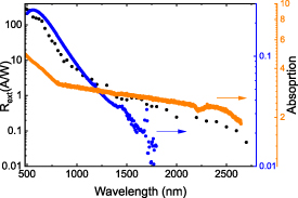
Figure 12. Spectral Rext of SLG/BP PDs (black circles), experimental absorption of SLG/BP on quartz (orange circles), and theoretical absorption of SLG/BP on Si/SiO2 (blue circles) using the BP refractive index extracted from the absorbance of LPE BP with the KK relations [160], as a function of excitation wavelength.
Download figure:
Standard image High-resolution imageMetal-SLG-metal PDs were reported with Rext of few mA W−1 at 633 nm [155] and 1550 nm [156]. The difference in Rext between these and our SLG/BP PDs is attributed to the contribution of the BP photoactive layer. To get a better understanding of spectral response versus wavelength, we perform optical simulations. We extract the BP refractive index from the solution absorbance of LPE BP, figure 4(a). Specifically, transmission in solution can be defined either by the absorbance ( =
=  as Tr
= 10
as Tr
= 10 ) or by the optical depth as e−al
[157, 158], where l is the cuvette length and a = a
) or by the optical depth as e−al
[157, 158], where l is the cuvette length and a = a c/ρ, a
 = 4πK
= 4πK /λ is the BP bulk absorption coefficient, KBP
is the imaginary part of the BP refractive index, ρ is the BP density (2340 gL−1 [159]), and λ is the incident wavelength. We assume BP flakes randomly oriented, thus seek to extract the average refractive index [160]. Then, KBP
=
/λ is the BP bulk absorption coefficient, KBP
is the imaginary part of the BP refractive index, ρ is the BP density (2340 gL−1 [159]), and λ is the incident wavelength. We assume BP flakes randomly oriented, thus seek to extract the average refractive index [160]. Then, KBP
=  /4πlog10(e) and the real part of the average refractive index is found by applying the Kramers–Kronig (KK) relation [160],
  = 1 + 2π−1

 , where
  denotes the principal value of the integral and w is angular frequency. The absorbance data of figure 4(a) are truncated at UV = 300 nm, due to the cuvette absorbance ∼300 nm [161], making our nBP
extraction qualitative, because of the finite integration range. We use the extracted BP refractive index in Fresnel equation calculations [162] to estimate the absorption of SLG/BP on Si/SiO2. The SLG refractive index is modelled by the Kubo conductance [163] at RT and EF
= 0.38 eV, as estimated by the Raman measurements in figure 6. Due to the fluctuations in absorbance beyond 1700 nm, figure 4(a), we do not extract refractive index for BP beyond 1700 nm. The experimental absorption of inkjet-printed BP/SLG on quartz is plotted in figure 12. This follows the experimental and theoretical absorption spectra of SLG/BP films, i.e. drop of both R
denotes the principal value of the integral and w is angular frequency. The absorbance data of figure 4(a) are truncated at UV = 300 nm, due to the cuvette absorbance ∼300 nm [161], making our nBP
extraction qualitative, because of the finite integration range. We use the extracted BP refractive index in Fresnel equation calculations [162] to estimate the absorption of SLG/BP on Si/SiO2. The SLG refractive index is modelled by the Kubo conductance [163] at RT and EF
= 0.38 eV, as estimated by the Raman measurements in figure 6. Due to the fluctuations in absorbance beyond 1700 nm, figure 4(a), we do not extract refractive index for BP beyond 1700 nm. The experimental absorption of inkjet-printed BP/SLG on quartz is plotted in figure 12. This follows the experimental and theoretical absorption spectra of SLG/BP films, i.e. drop of both R and absorption with increasing wavelength, indicating Rext follows the absorption spectra of the light-absorbing photoactive material.
The temporal response of our PDs is then measured with a MSO9404A Mixed Signal Oscilloscope, figure 13(a). The time response in figure 13(a) reaches saturation at ∼3.8 µA, as shown by the horizontal dashed line. We thus fit the temporal response decay in figure 13(a) with [72]: I(t) = A0.exp(-t/τlife) + B, where A0 is the initial current, τlife
is the response time and B a constant. We get a response time ∼50 ms, two orders of magnitudes faster than the LPE BP/CVD SLG PD of reference [66], consistent with other LPE based PDs [44, 164], but two orders of magnitude slower than the Schottky junction PDs of reference [41], with lower R 164 mA W−1 at 450 nm, due to lack of photoconductive gain, but faster response time ∼550 µs, because of the Schottky diode characteristics at the Si/SLG/BP interfaces [41].
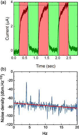
Figure 13. (a) Time response at 642 nm. The green zones indicate light off (dark condition), the red zone, light on. (b) Noise spectral density.
Download figure:
Standard image High-resolution imageBy applying V , transferred photogenerated h drift to the drain with a timescale τtransit [6]:
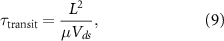
where L = 60 µm is the length of channel, and  1700 cm2V−1s−1. We thus get
  37 ns, resulting in a photoconductive gain [6]:
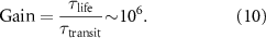
The dependence of Rext on  explains the decrease in R
 when the optical power increases. The decrease in Rext suggests an increase of τtransit
and/or decrease of τlife. The increase of τtransit is likely due to increase in scattering of photogenerated carriers in the channel with increase in optical power [165]. Auger recombination induced by increasing power can also increase the photogenerated charges recombination rate, reducing τlife
[165]. The gain can be further defined as the ratio of photogenerated currents recirculating in the SLG channel to the injected h from BP to SLG [68]:
when the optical power increases. The decrease in Rext suggests an increase of τtransit
and/or decrease of τlife. The increase of τtransit is likely due to increase in scattering of photogenerated carriers in the channel with increase in optical power [165]. Auger recombination induced by increasing power can also increase the photogenerated charges recombination rate, reducing τlife
[165]. The gain can be further defined as the ratio of photogenerated currents recirculating in the SLG channel to the injected h from BP to SLG [68]:
where  is the concentration per unit area and per unit time of the injected h.
  is equal to the trapped e concentration per unit area and per unit time in BP, related to a charge neutrality point shift
  in the transfer characteristics (Id
versus Vg
). To calculate
in the transfer characteristics (Id
versus Vg
). To calculate  , we consider the potential balance in the metal-dielectric-SLG structure. Vg
creates a potential drop
, we consider the potential balance in the metal-dielectric-SLG structure. Vg
creates a potential drop  so that [6, 132]:
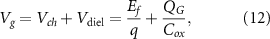
where QG
is the charge concentration.  , with pch
the charge carrier concentration per unit area in the channel induced by Vg
. Any variation in pch
changes Qg
and Vg
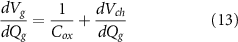
. The derivative of Vg
with respect to Qg
gives:
, with pch
the charge carrier concentration per unit area in the channel induced by Vg
. Any variation in pch
changes Qg
and Vg
. The derivative of Vg
with respect to Qg
gives:
which results in:
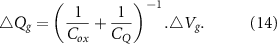
To find QG
and  , Cox
and CQ
are needed.
, Cox
and CQ
are needed.  . From equation (7), we get
  6
6 . Therefore,
  varies from ∼2.6
 to
to  for optical power 620nW to 612 µW at
  . Then, from equation (11), we get Gain
  , in agreement with equation (10).
We then evaluate the detectivity  [
[ or Jones]. This relates the performance of PDs in terms of R
 to A
to A , allowing the comparison of PDs with different A
 [6]:
[6]:
where B is the electrical bandwidth(Hz), defined as difference between the upper and lower frequencies of Rext, and NEP is the noise equivalent power (i.e. the power that gives a signal to noise ratio of one in a 1 Hz output bandwidth [6, 166]):
where  is the dark noise current, i.e. the current that exists when no light is incident on the PD [6]. The noise [A/
 ] is measured in the time domain, by collecting the trace on an oscilloscope, with subsequent Fourier transform in order to analyze the data in the spectral domain. Figure 13(b) plots the 1/f noise (where f is the frequency). 1/f is the noise density (noise power per unit of bandwidth [dBm.Hz
 ] [6]), due to charge traps and defects [6]. At 4 Hz, ∼5 times less than the cut off f, i.e. the f at which the detector R
 decreases by 3 dB [6], we get NEP
  and D
and D 2×10⁷Jones. The noise current in the shot noise limit (due to generation-recombination of e-h pairs and resistive current paths in PDs [6]) is defined as
  [166], where the total dark current combines the contribution of the unamplified SLG current Idark(SLG), and the amplified injection current from BP, Idark(BP) , due to the thermal excitation of charge carriers in dark. The latter is orders of magnitube smaller compared to Idark(SLG)∼200mA. Therefore, following the methodology presented in reference [166], in our devices the shot noise limited noise current is in = (2qIdark(SLG))1/2. Thus, in the shot noise limit, we can write
  as [6]:
Equation (17) gives  1011 Jones, ∼3 times higher than reference [45] for inkjet-printed graphene/MoS2 PDs. It is also ∼3-4 orders of magnitude higher than reference [47] for PDs based on inkjet-printed MoS2. We note that gain was not included in the D* calculations in references [46, 47], which may have led to a D* overestimation. Thus, our inkjet-printed PDs are suitable for detecting weak light intensities which compete with the detector noise [6].
2.3. SLG/BP on fabric
In wearable applications, inkjet lithography has advantages over EBL and other lithography techniques for patterning and device fabrications because of textiles' porous [167], rough [167] and non-conductive structure [167], which makes these lithography techniques not suitable. To showcase this, we fabricate PDs on polyester fabric, because of its durability against Sun exposure [168], wrinkling [168] and shrinking [169], and common use (∼52 of the synthetic textile market in 2018 [167, 170]). Since the surface roughness of textiles affects the electrical conductivity [171, 172], we planarize the surface by reducing the roughness. To do so, we rod coat polyurethane (PU) 10 times to reduce the root mean square (RMS) roughness from ∼50
  to
to  . We then transfer SLG on PU coated polyester fabric using a similar procedure as for Si/SiO2. After removing PMMA, a PVP ink is inkjet-printed as mask on SLG to pattern a
  channel. SLG is then etched via RIE, followed by removal of PVP with water.
Figure 14 shows the Raman spectra of 2 SLG on PU coated polyester fabric. The PU coated polyester fabric has two bands ∼2935 and ∼2845 cm−1 attributed to asymmetric and symmetric C-H stretching vibrations of CH2 groups [173, 174], figure 14(c). The peak ∼1615 cm−1 can be ascribed to -C = C- stretching vibrations of aromatic rings [175, 176], figure 14(b). The peak ∼1442 cm−1 can be assigned to C-H deformation vibrations of CH2 groups [173, 176] and that ∼1251 cm−1 to coupled C-N and C-O vibrations of urethane [173, 176], figure 14(b). The spectrum of SLG on fabric has Pos(G)∼1596.9 cm−1, FWHM(G)∼14.4 cm−1, figure 14(b), Pos(2D)∼2693.3 cm−1, FWHM(2D)∼56.6 cm−1, figure 14(c). I(2D)/I(G) and A(2D)/A(G) are ∼1.5 and 5.8, indicating a p-doping of E 270 meV [132, 133], which corresponds to a carrier concentration ∼4.33×1012 cm−2 [132]. I(D)/I(G)∼1.03 corresponds to defect density ∼4.6×1011cm−2 [134, 135] for excitation energy 2.41 eV and EF
= 270meV. For the EF
derived from A(2D)/A(G), Pos(G) should be ∼1589.2 cm−1 for unstrained SLG [132]. In our experiments, Pos(G)∼1596.9 cm−1, which implies a contribution from uniaxial (biaxial) strain ∼0.33
270 meV [132, 133], which corresponds to a carrier concentration ∼4.33×1012 cm−2 [132]. I(D)/I(G)∼1.03 corresponds to defect density ∼4.6×1011cm−2 [134, 135] for excitation energy 2.41 eV and EF
= 270meV. For the EF
derived from A(2D)/A(G), Pos(G) should be ∼1589.2 cm−1 for unstrained SLG [132]. In our experiments, Pos(G)∼1596.9 cm−1, which implies a contribution from uniaxial (biaxial) strain ∼0.33 (0.12
(0.12 ) [136], comparable to the uniaxial (biaxial) strain ∼0.36
 (0.13
(0.13 ) of SLG on Si/SiO2.

Figure 14. (a), (b), (c) Raman spectra at 514.5 nm of fabric (amber), 2 SLGs on fabric after patterning and PVP removal(red), parylene C on fabric (blue), and 2 SLGs/BP with encapsulation of parylene C (green).
Download figure:
Standard image High-resolution imageWe then inkjet print electrodes with the Ag ink. The sample is annealed at ∼100 ∘C for ∼2 h to remove residual solvent (triethylene glycol monomethyl ether). We transfer two SLG to have  2.1 KΩ, comparable to transferred CVD SLG previously reported for polypropylene coated fabrics [172]. BP is then inkjet-printed on the channel layer. Figures 15(a) and (b) are optical and SEM images of PDs on polyester fabric. Figure 15(c) plots the current–voltage characteristic in dark, which shows an Ohmic resistance (
 ) between inkjet-printed electrodes and SLG channel. We then characterize R
 at 488 nm for P = 1.1 mW. Figure 15(c) shows that the current increases under illumination. We get R
 6 mA W−1 at 488 nm.
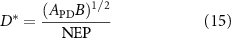
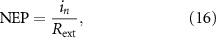
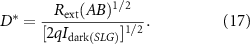
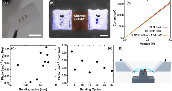
Figure 15. (a) SLG/BP PD array on polyester fabric. Scale bar 5 mm. (b) SEM of PD on polyester fabric. Scale bar 200 µm. (c) Current as function of V
 for SLG and SLG/BP in dark, and SLG/BP under illumination at 488 nm for
  . (d) Iphoto normalized to that measured on flat PD, as a function of bending radius. (e) Iphoto normalized to that on flat PD as a function of bending cycle. (f) Schematic of bending setup. Arrows indicate applied force on grips, the bent SLG/BP PD is drawn in mint green between the grips, y is the height at the chord midpoint, and x is the chord circumference.
Download figure:
Standard image High-resolution image
The Raman spectrum of BP coated on SLG on fabric is in figure 14(a). Pos(G)∼1587.4 cm−1, FWHM(G) broadens from ∼14.4 cm−1 to ∼15.6 cm−1, figure 14(b), Pos(2D)∼2687.5 cm−1, FWHM(2D) narrows from ∼56.6 cm−1 to ∼32.5 cm−1, figure 14(c). I(2D)/I(G) and A(2D)/A(G) are ∼5.1 and 10.7, indicating n-doping with E 100meV [132, 133] which corresponds to a carrier concentration ∼0.7×1012cm−2 [132]. I(D)/I(G) ∼5.2 gives a defect density ∼1.4×1012cm−2 [134, 135] for excitation energy 2.41 eV and E
 100 meV. EF
estimated from A(2D)/A(G) would imply Pos(G)∼1583.8 cm−1 for unstrained SLG [132]. However, in our experiments Pos(G)∼1587.4 cm−1, which would imply a contribution from uniaxial (biaxial) strain ∼0.15
100 meV. EF
estimated from A(2D)/A(G) would imply Pos(G)∼1583.8 cm−1 for unstrained SLG [132]. However, in our experiments Pos(G)∼1587.4 cm−1, which would imply a contribution from uniaxial (biaxial) strain ∼0.15 (0.05
(0.05 ) [136].
Bendable devices, able to coordinate with body motions, such as arms' and legs' bending or extension, are appealing for wearable electronics. Thus, we test Iphoto as function of bending using a Deben Microtest setup, figure 15(f). The bending radius Rb is defined as [177]:
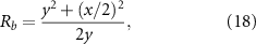
where y is the height at the chord midpoint and x is the chord circumference connecting the two ends of the grips, figure 15(f). To compare the performance at different Rb
, the photocurrent at each Rb
( ) is normalized to that measured in flat conditions (
 ). Figure 15(d) shows a change
  of
of  for Rb
from flat to 25 mm. This is comparable to that reported for LMs-based PDs, such as InSe PDs on PET [178], but in reference [178] Rext was ∼50
for Rb
from flat to 25 mm. This is comparable to that reported for LMs-based PDs, such as InSe PDs on PET [178], but in reference [178] Rext was ∼50 that of Rb
= 30 mm [178]. Comparable Rb
was reported for flexible ZnO nanowires [179], with on/off ratio ∼11×104 (I
that of Rb
= 30 mm [178]. Comparable Rb
was reported for flexible ZnO nanowires [179], with on/off ratio ∼11×104 (I 120nA) under ∼4.5 mWcm−2 of UV light (R
 not reported) [179]. However the operating voltage (1 V) of our PDs is 3 times smaller than that in reference [179], making them more suitable for wearable applications, and lowering power. The SLG/BP PDs performance as a function of bending cycles, where 1 bending cycle is set at R
 35 mm, is in figure 15(e). Our PDs retain
  of
of  for up to 30 cycles, comparable to what previously reported for CVD based MoS2/SLG PDs on PET [180], making our approach promising for wearable and flexible applications.
3. Discussion
Our PDs on Si/SiO2 have Rext up to ∼337A W−1 at 488 nm for 1 V bias and work in the range ∼488 nm–2.7 µm. Reference [181] prepared PDs by depositing ∼30 nm thick WS2 by rubbing WS2 powder against a polycarbonate substrate. Then, Au(100 nm)/Ti(5 nm) electrodes were made using e-beam evaporation through a shadow mask. The WS2-based PDs showed R 144 mA W−1 at 625 nm and V
 10 V, worse than ours, because of the photoconductive gain enhancement in our inkjet-printed hybrid SLG/BP PDs. Reference [182] presented WS2-based PDs using ∼4 nm WS2 fabricated via RF magnetron sputtering, with R
 1.68 mA W−1 at 405 nm [182]. This is worse than ours because of the photoconductive gain mechanism in our hybrid SLG/BP PDs. Reference [183] measured R
 0.16 A W−1 at 405 nm in self-powered PDs based on oxidized WS2(O-WS2)/WS2 heterojunctions, where ∼7.2 nm WS2 was transferred onto Si/SiO2 by polydimethylsiloxane (PDMS)-assisted micromechanical exfoliation. Photoresist was then spin-coated on WS2 via e-beam PHL, followed by oxygen plasma irradiation to form selective oxidation regions. Then, Au(100 nm)/Ti(10 nm) electrodes were prepared by PHL and electron beam deposition [183]. The fabrication process is more complex than ours, and the resulting R
 is ∼2000 times lower, since no bias is applied through source and drain electrodes to dissociate photogenerated charges. Reference [184] used spin-coated carbon QDs on CVD 1 L-MoS2 to achieve R
 377 A W−1 at 360 nm and 5 V. While R
 is comparable to ours, the PDs in reference [184] operated at 5 V and only between 300-700 nm, due to the spectral coverage of the carbon QDs [184], while our PDs work at 1 V from 488 nm to 2.7 µm. Reference [185] reported MoS2-based PDs, prepared by abrasion of MoS2 crystals (thickness ∼15–25 µm) on the substrate, resulting in R
 1.5 µ A W−1 at 660 nm and V
 20 V. R
 and operation voltage are worse than ours, because of our photoconductive gain, combined with the use of BP as photoactive material. To the best of our knowledge, our SLG/BP PDs on Si/SiO2 have the highest R
 amongst inkjet-printed LM-based PDs, and our operation wavelength range (488–2700 nm) is the broadest, as summarized in table 1.
For SLG/BP PDs on fabric we get R 6 mA W−1 at 488 nm, i.e. ∼56 000 less than on SLG/BP PDs on Si/SiO2. This R
 decrease is expected, since the photogenerated h in the BP VB experience weaker electric fields at the SLG/BP interface (p-doping ∼270 meV) compared to the SLG/BP interface (n-doping ∼360 meV) on Si/SiO2. Moreover, µ for SLG on fabric is lower than that on Si/SiO2, and the channel in our PDs on fabric is ∼8 times larger than on Si/SiO2. Rext also decreases when the optical power increases, due to the increase in scattering of photogenerated carriers in the channel [165], and Auger recombination induced by increasing power [165].
To the best of our knowledge, there is no report of inkjet-printed textile PDs based on LMs. Our Rext is ∼6 times higher than inkjet-printed SLG/WS2 PDs on PET [42], and one order of magnitude higher (R
 0.11 mA W−1 at 405 nm [100]) than CVD SLG based PDs on flexible (acrylic) substrates [100].
4. Conclusions
We reported an inkjet printing-based approach to prepare PDs, combining CVD SLG and binder-free LPE BP. The devices have Rext up to ∼337 A W−1 at 488 nm, and ∼48 mA W−1 at 2700 nm, with operation voltage  . We used this to make flexible PDs on polyester fabric. These PDs were investigated as function of bending radius and cycles. The responsivity, flexibility, and low operation voltage of our PDs makes them attractive for wearable and low-power optoelectronic applications.
Acknowledgments
We acknowledge funding from EU grants Graphene Flagship, HiGraphInk, NanoGraphInk, Neurofibres, Graph-X, ERC Grants Hetero2D, EPSRC Grants EP/K01711X/1, EP/K017144/1, EP/N010345/1, EP/L016087/1, EP/V000055/1, EP/P00119X/1, EP/X015742/1, DSTL, ISF Grant 1732/18.
Data availability statement
All data that support the findings of this study are included within the article (and any supplementary files). DOI: https://doi.org/10.17863/CAM.91144