

Abstract
V2CTx shows a low ion diffusion barrier, while the multiple oxidation states of vanadium allow V2CTx to participate in multi-electron redox reactions, which demonstrates a greater potential for electrochemical energy storage applications. However, the lateral arrangement of V2CTx lamellae tends to cause the accumulation and collapse of the structure. Herein, the two-dimensional layered V2CTx is modified with Ag+ and Cu2+, the V2CTx/Ag/Cu composite is successfully prepared. The Ag nanoparticles (NPs) and Cu NPs grown between the layers of V2CTx can effectively suppress the accumulation of the lamellae and ensure the smooth transfer of electrolyte ions and electrons between the layers. Meanwhile, the doping of Ag NPs and Cu NPs can enlarge the interlayer spacing of V2CTx, which can expose more active contact sites for electrolyte ions, shorten the diffusion path of electrolyte ions, and effectively improve the electrochemical performance of V2CTx. The Ag NPs and Cu NPs agglomerate in the delamination of V2CTx to form a conductive channel covering multiple layers, which facilitates cross-layer electron transfer and reduces the internal resistance of the V2CTx/Ag/Cu composite. Basis on the above reasonable structural designs, the internal resistance of the V2CTx/Ag/Cu composite is only 0.72 Ω, showing excellent diffusion ability of K+. The result represents a new step forward in exploring the electrochemical properties of two dimensional materials of V2CTx.
Export citation and abstract BibTeX RIS
1. Introduction
Energy consumption has accelerated the development of energy technologies, and there is an urgent need for green and renewable energy sources with efficient energy storage devices. The development of electrode materials play an important role, the low-cost, high specific capacity, low polarization and stable electrode materials are sought-after [1, 2]. Two-dimensional transition metal carbides, nitrides or carbon-nitrides are collectively referred to as MXenes [3]. MXene shows a high specific surface area, so the active sites on the surface can contact the electrolyte more fully, and the dense active sites can effectively reduce the diffusion path of electrolyte ions, thus improving its performance [4, 5]. The carbon atomic layers in the MXene material enable rapid electron transfer on the surface of the carbon layer, and the transition metal atomic layers give the potential pseudo-capacitive properties, making MXenes materials show excellent electrode materials for electrochemical energy storage devices [6]. Since the Ti3C2Tx was successfully prepared by Naguib et al in 2011 using hydrofluoric acid as etching agent [7], MXene materials have developed very rapidly for electrochemical energy storage [8, 9]. V2CTx is one kind of the various MXenes, which shows a smaller ion diffusion barrier compared to Ti3C2Tx , while the multiple oxidation states of vanadium allow V2CTx to participate in multi-electron redox reactions [10, 11]. Therefore, V2CTx shows a large potential for electrochemical energy storage applications.
MXenes show the advantages of large specific area, large layer spacing, excellent electrical conductivity, fast ion and molecular diffusion, easily tunable structure and hydrophilicity [12]. However, due to the interaction of hydrogen bonding and van der Waals forces, the layers of MXene are prone to accumulation and collapse, which leads to a large loss of active sites and hinders the diffusion of electrolyte ions and electron transfer, thus severely limiting the electrochemical performance [13]. The MXenes can be intercalated by metal cations (Ag+, Mn2+, Cu2+), CNT and metal oxide as spacer support the layers, which can effectively prevent MXene flakes from accumulation and collapse, thereby improving the electrochemical performance [14–16]. Huo et al [17] prepared the F-Ti3C2Tx @Ag composite by modifying the two-dimensional layered F-Ti3C2Tx with Ag+. It was found that the discharge specific capacity was about 150 mAh g−1 after 2000 cycles at a current density of 0.5 Ag−1, which showed the long cycle life and high specific capacity. Zou et al [18] obtained MXene/Ag composite by reducing aqueous silver nitrate solutions. Experiment showed that the composite can withstand more than 5000 cycles at 1–50 C without capacity decay, exhibiting a long cycle life of large capacity. Liang et al [19] used a simple redox method to synthesize Ti3C2Tx /Ag composite. The results showed that Ti3C2Tx /Ag samples with low charge transfer resistance exhibited pseudocapacitance and cell properties. Lv et al [20] formed the composite two-dimensional layered structure of V2C@Se by calcining selenium and V2C. It was found that due to the participation of Se, the cathode material could reversibly provide an initial discharge specific capacity of 402.5 mAh g−1 at 1 A g−1 and maintain 119.8 mAh g−1 after 1000 cycles. Wei et al [21] proposed the Mn2+ intercalation strategy to optimize the sodium storage performance of V2C. The result showed that the V2C@Mn electrode showed a high specific capacity of 425 mAh g−1 at a current density of 0.05 A g−1, and the capacity remained 70% after 1200 cycles. Ren et al [22] obtained flexible self-loaded porous MXene electrodes using Cu2+ cation catalysis and acid washing. The porous structure shortened the diffusion path of lithium ions and improved the energy storage performance by the application of active sites on the surface of MXene. Allah et al [23] prepared a new heterostructured MXene (Ti3C2Tx )/nitrogen-doped ordered mesoporous carbon (NOMC) hybrid. The results showed a high weight capacitance of 329 F g−1 and a bulk capacitance of 823 F cm−3 when it was used as an electrode. In addition the Ti3C2Tx NOMC composite exhibits excellent rate capability and good cycling stability. Pan et al [24] a new V2CTx MXene/NiV layered double hydroxide (V2CTx /NiV-ldh) composite using in situ synthesis. It showed a specific capacitance of 1658.19 F g−1 at 1 A g−1 when used as an electrode, and had good stability with a capacity retention of 80.95% after 10 000 cycles. Zhang et al [25] synthesized alkaline V2CTx with accordion-like structures by etching in a mild mixed solution followed by alkaline treatment with sodium hydroxide solution. The results showed that the alkaline V2CTx sensor exhibited higher gas response (more than 80 times) to 50 ppm NO2 compared to the V2CTx sensor driven by surface adsorption.
When Ag+ and Cu2+ are introduced into V2CTx , these metal ions will attach to the surface of V2CTx under the attraction of surface terminating functional groups and further be reduced to Ag nanoparticles (NPs) and Cu NPs. Ag NPs and Cu NPs will enter into the interlayer of V2CTx and act as the supports to protect its unique layered structure and ensure the diffusion of electrolyte ions in the interlayer. Moreover, the presence of Ag NPs and Cu NPs increases the layer spacing of V2CTx , exposing more active sites to promote the binding of electrolyte ions, which improving the electrochemical performance.
In this paper, V2CTx is modified by using metal cations Ag+ and Cu2+. The Ag NPs and Cu NPs obtained by reduction not only reduce the influence of surface functional groups on the electrochemical properties of V2CTx , but also enter the interlayer to prevent the stacking and collapse of the structure. The Ag NPs enter the interlayer of V2CTx and effectively protect its unique layered structure, which accelerates the diffusion of electrolyte ions. The formation of Cu NPs not only promotes the formation of Ag NPs, but also forms a good conductive channel in combination, realizes the cross-layer transport of electrons, and improves the efficiency of electron transfer. Moreover, Cu NPs increase the interlayer spacing, which exposes more active sites for V2CTx , thereby enhancing the ion and electron transfer efficiency in the electrolyte solution. The synergistic effect of Ag NPs and Cu NPs effectively increases the electron transfer rate and the permeation efficiency of electrolyte ions, thus improving the electrochemical performance of V2CTx .
2. Experimental
2.1. Materials
V2AlC (>99%) and HF (49%) are supplied by Foshan Xinen Technology Co. AgNO3 solution (0.01 mol l−1) is offered from Jiangbiao Testing Technology Co. Propanol (>99.7%) and Cu(NO3)2 (>99%) are provided by Urumqi Xinyuancheng Commercial Co. All the above materials are of analytical purity grade.
2.2. Preparation of V2CTx (M-II)
V2CTx is obtained by chemical etching of V2AlC (M-I) using HF. Firstly, HF (50 ml, 49%) solution is dispersed into PTFE vessels, and V2AlC (5 g) is added and etched at 40 °C and 700 rpm under magnetic stirring for 48 h. The precipitate obtained by centrifugation at 10 000 rpm for 5 min is repeatedly washed with deionized water until the pH of the solution containing the precipitate reached 7. The precipitate fraction is filtered through a water pump and a filtering flask. It is placed in a vacuum drying oven at 60 °C for 6 h. Finally, the dried V2CTx (M-II) removes and grounds into powder and stores in a drying dish. The experiment is protected by passing Ar gas during the experiment.
2.3. Preparation of V2CTx /Ag (M-III)
V2CTx (1 g) is dispersed in propanol solution (50 ml) by ultrasound. AgNO3 solution (100 ml, 0.01 mol l−1) is slowly added to the uniformly dispersed suspension with continuous stirring at 60 °C for 30 min, thus obtaining the V2CTx /Ag solution. The precipitate is obtained using a high-speed centrifuge (5000 rpm, and 5 min) and washed once with deionized water and then processed by vacuum pumping equipment. The obtained precipitate is put into a vacuum drying oven and dried at 60 °C for 6 h. The obtained V2CTx /Ag (M-III) is ground into powder form and put into a glass vial for drying and storage.
2.4. Preparation of V2CTx /Ag/Cu (M-IV)
V2CTx /Ag (1 g) and Cu(NO3)2 (5 g) are put into a gas wash bottle containing propanol solution (50 ml) to obtain a uniformly dispersed suspension by ultrasonic device. The dispersed Cu(NO3)2 solution is slowly added to the vial containing V2CTx /Ag dispersion and stirred magnetically at 60 °C for 60 min. The complexes are washed with deionized water by high speed centrifugation (5000 rpm, and 5 min). The obtained complexes are dried in a vacuum drying oven at 60 °C for 6 h. The dried V2CTx /Ag/Cu (M-IV) is ground into powder by mortar, then store in a glass vial. The test is carried out under protective gas or vacuum conditions in order to avoid oxidation of V2CTx . The preparation process of M-IV is shown in figure 1.

Figure 1. Schematic illustration of the preparation of M-IV.
Download figure:
Standard image High-resolution image2.5. Analysis and characterization
The microscopic morphology and dimensions of the materials are observed by scanning electron microscopy (SEM). The crystal structures of M-I, M-II, M-III and M-IV are investigated by x-ray diffractometer using Cu Kα irradiation (λ = 1.5406 Å) at 40 kV, 20 mA over the 2θ range from 5° to 80°. X-ray photoelectron spectroscopy (XPS) is employed to analyze the structural composition and elemental state of the samples. High resolution transmission electron microscopy (FEI TALOS F200X) is used to study the microscopic morphology and structural composition of the sample internals. IR Nicolet iS50 infrared spectrometer is recruited to analyze the changes in the functional groups of the samples. Raman spectroscopy is performed using a laser confocal Horiba HR800 excited by a 532 nm laser. Electrochemical tests are performed by a Shanghai Chenhua CHI660E electrochemical workstation.
2.6. Electrochemical measurements
The electrochemical performance of the electrode materials is tested in a 6 M KOH electrolyte using a three-electrode system with the above electrode materials as working electrodes. Platinum sheet and Hg/HgO electrodes as counter and reference electrodes, respectively. Cyclic voltammetry (CV) is performed at room temperature using an electrochemical workstation (CHI660E, Shanghai Chenhua). The CV test is carried out in the voltage window of −1.1 to −0.4 V with scan rates of 1, 5, 10 and 20 mV s−1. The EIS test is performed at open circuit voltage with a frequency range from 10−2 Hz to 105 Hz and an amplitude of 5 mV. The potentials mentioned in this paper are all scaled from Ag/AgCl conversion to reversible hydrogen electrode (RHE) using the equation E (RHE) = E (Ag/AgCl) + 1.02 V in 0.6 M KOH.
In addition, the relationship between current and scan rate in its CV curve distinguishes the two, with the current of all electrodes consisting of diffusion-controlled and surface-controlled (capacitive) components [26], which can be expressed as:


where a is a coefficient, b = 1 stands for surface-controlled process completely, and b = 0.5 for diffusion-controlled one completely.
The capacitance contribution of M-IV composites at different sweep speeds can be calculated from the following equations (1) and (2) [27, 28]:

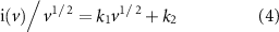
where k1 and k2 are adjustable values and ν is the specific voltage sweep speed. The first one is the capacitive control contribution (k1 v) and the second one is the diffusive control contribution (k2 v1/2). By plotting i/v1/2 vs v1/2, it is possible to clearly distinguish between diffusivity and capacitance.
The equation for calculating the capacitance of M-IV composites using CV curves is as follow [29]:
where C, I, ΔV, v and m refer to the specific capacitance (Fg−1), the discharge current (A), the total potential deviation (V), the scan rate (mV s−1), and the mass of active materials in electrodes (g), respectively.
3. Results and discussion
3.1. Microstructure
In order to facilitate the description of the different materials, the V2AlC, V2CTx , V2CTx /Ag and V2CTx /Ag/Cu composites are referred to as M-I, M-II, M-III and M-IV, respectively. The crystal structures of M-I, M-II, M-III and M-IV are investigated by XRD. Figure 2(a) shows the XRD pattern of M-Ⅰ, M-II, M-III and M-IV. There are two peaks of high intensity appear at 13.468° and 41.264°, corresponding to the (002) and (103), which are characteristic crystal structures of V2AlC. The intensity of the (002) peak is greatly diminished and the peak (103) disappeared, as well as the appearance of the characteristic peak of high intensity of peak (121) representing V2CTx [30, 31], which indicates the peeling of the Al layer from the M-I and the V2CTx prepares successfully. There is new characteristic peak representing the crystal structure of Ag can be observed at 38.12° in the XRD pattern of M-III [32], indicating that Ag NPs successfully formed. It can be seen from the M-IV that there is a new diffraction peak appears at 44.46° after the addition of Cu(NO3)2, corresponding to the characteristic crystal structure of Cu [33]. After loading with Ag NPs and Cu NPs, the intensity of some diffraction peaks of M-IV decreased limitedly or even disappeared.

Figure 2. (a) The XRD pattern of M-I, M-Ⅱ, M-Ⅲ and M-IV. (b) Layer spacing of M-II, M-Ⅲ and M-IV. (c) Particle size distribution of M-Ⅲ and M-IV.
Download figure:
Standard image High-resolution imageIn order to investigate the effect of the entry of Ag NPs and Cu NPs sequentially on the interlayer of V2CTx , the layer spacing of M-II, M-III and M-IV composites are calculated by the Bragg equation (2dsinθ = nλ) [34]. Figure 2(b) reveals the variation of the layer spacing of M-II, M-III and M-IV composites. It can be seen from figure 2(b) that the average values of the layer spacing for M-II, M-III and M-IV composites are 0.176 nm, 0.193 nm and 0.215 nm, respectively. The layer spacing of M-III is 0.193 nm, which is relatively increased compared with that of M-II. Some Ag NPs enter the interlayer of V2CTx as a support to prevent the collapse of V2CTx and further increase the layer spacing. The layer spacing of M-IV increases to 0.215 nm, forming a larger surface area with the active site [35] and providing more vacancy binding sites for the adsorption of Cu2+. Meanwhile, small Ag NPs enter the intermediate layer of V2CTx , leaving more binding sites for Cu2+.
The variation of the average particle size of Ag NPs in M-III and M-IV composites and the particle size of Cu NPs in M-IV composite are calculated by the Scherrer formula (D = 0.9λ/βcosθ) [36]. Where D is the particle size, λ is the x-ray wavelength, which is equal to 0.154, θ is the diffraction angle, and β is the half-peak width. The grain sizes of Ag NPs in M-III and M-IV were 33.6 nm and 48.7 nm, respectively, as seen in figure 2(c). The reason for the difference was the increase in the layer spacing of V2CTx , which led to more abundant active sites and further attraction of Ag+, resulting in an increase in their grain size. A further increase in the number of Ag NPs leads to agglomeration phenomena, resulting in an increase in the peak Ag intensity, an increase in the crystallinity of Ag NPs, a decrease in the measured half-peak width [37], and ultimately an increase in the average diameter of Ag NPs.
To investigate the chemical structure of the M-IV composite, it is further characterized by Raman and Infrared spectroscopy, and the results are shown in figure 3. Figure 3(a) shows the Raman spectra of the M-IV composite. Similar to the conclusions obtained from theoretical calculations by other scholars [38, 39], there are three peaks at ∼479 cm−1, ∼538 cm−1 and ∼695 cm−1, which can be attributed to the active vibration modes of terminated M-IV. The peak locates at ∼479 cm−1 can be attributed to the V2C(OH)2. The peaks locate at ∼538 cm−1 and ∼695 cm−1 correspond to the out-of-plane (A1g) vibrations of V in V2CF2 and V2CO(OH). The Eg model and A1g model are attributed to the in-plane and out-of-plane vibrations of V atoms, respectively. The presence of the surface functional groups attracts the Ag+ and Cu2+ and promotes the formation of Ag NPs and Cu NPs, preventing the accumulation of V2CTx and ensuring the transfer of electrons and ions between the layers. Figure 3(b) shows the Fourier infrared spectra of the M-IV composite. The characteristic absorption peak of the V–O bond at 655 cm−1 indicates that V2CTx introduced –O termination functional groups on the surface and oxidation occur during the etching and doping process. The characteristic peak of M-IV locates at 1158 cm−1 is derived from the stretching vibration of the C–O bond. There is a significant peak appears at 1625 cm−1, which is a bending vibration absorption peak belonging to C–OH. It can be observed in figure 3(b) that a broad and strong absorption peak appears near 3438 cm−1, which is due to the stretching vibration peak of –OH, indicating that termination functional groups such as –OH is introduced on the surface of V2CTx . It provides a favorable occasion for the adsorption of Ag+ and Cu2+ and further reduction to Ag NPs and Cu NPs and consumes some functional groups further improve the electrochemical properties. The uniform growth of Ag NPs and Cu NPs between V2CTx layers effectively prevents collapse and accumulation, combining with each other to form conductive channels that allow rapid passage of electrons, resulting in excellent electrochemical properties of the M-IV composite.

Figure 3. (a) The Raman spectra of M-IV. (b) The Fourier infrared spectra of M-IV.
Download figure:
Standard image High-resolution imageThe changes in the microstructure of Ag NPs and Cu NPs after entering the structure of V2CTx are shown in figure 4. The SEM image of the M-I is shown in figure 4(a). It is shown that M-I is a hierarchical block of micron size, corresponding to its dense ternary lamellar structure. Figure 4(b) shows the SEM image of M-II. It can be observed in figure 4(b) that the dense layered block gradually distinguishes the layers and forms a two-dimensional stacking structure after the long time etching of HF. The layered structure of V2CTx provides the possibility to retain the internal conductive layer [40], thus offering the opportunity to prepare Ag NPs and Cu NPs in situ on the surface of V2CTx . Figures 4(c) and (d) show the SEM images of M-III. Figure 4(c) shows the distribution of Ag NPs on the surface of V2CTx . The electron exchange between the positively charged Ag+ and the negatively charged functional groups on the surface of V2CTx [41], leading to the formation of Ag NPs. A number of the Ag NPs enter the interlayer and interconnect to form pillars [42], protecting its unique layered structure, which is the basis for ensuring the electron operation and ion motion between the layers. It can be clearly seen from figure 4(d) that the Ag NPs adsorbing on the edges of V2CTx layering bridge to each other, forming a conductive channel that can shorten the electron transport path, further improving the electrochemical properties. Combined with the XRD part, it is obvious that the entry of Ag NPs increases the interlayer spacing of M-III composite, forming a larger surface area and more active sites. Figure 4(e) shows the elemental mapping of the M-III composite, and the Ag content in the structure reaches 1.29%, indicating that the Ag NPs are successfully adsorbed on the surface of V2CTx . Figure 4(f) shows the SEM image at low magnification of M-IV. For clear comparison, M-IV is selected with the same dimensions as in figure 4(c). The layered structure of M-IV is uniformly distributed with well-defined Cu NPs, and aggregation of Ag NPs occurs on the layered edges of V2CTx across multiple interlayers. Figure 4(g) shows a further enlarged view of figure 4(f). As can be seen in figure 4(g), Cu NPs not only grow during the delamination process of V2CTx , but also some of the Cu NPs enter the intermediate layers to prevent the structure from collapsing. Ag NPs and Cu NPs growing at the edges of the delamination aggregate, forming aggregation that encompass multiple interlayers of V2CTx . Figure 4(h) shows the SEM image at high magnification of M-IV. It can be clearly observed from figure 4(h) that the ordered distribution of Cu NPs at the edges of V2CTx and the Ag NPs aggregated between the layers combine with each other, not only entering into the layers to widen the layer spacing of V2CTx and exposing the larger active site-rich surface to the electrolyte solution, thus facilitating the diffusive movement of ions on the V2CTx surface and between the layers. The diameter of Cu NPs in figure 4(h) is about 34.3 nm, which differs from the 42.6 nm calculated earlier in the XRD section due to the fact that only some of the Cu NPs are visible in SEM, while the average particle size is calculated in XRD. It is observe that the particle size of silver in figure 4(h) exceeds 80 nm much larger than 48.7 nm XRD calculations, which is due to the aggregation of some of the Ag NPs, resulting in their larger crystal size. Figure 4(e) shows the elemental mapping of the M-IV composite, where the content of Ag elements increases to 4.06% relative to M-III and the content of Cu elements reaches 1.55% indicating that Cu NPs successfully enter into the structure of M-IV. The reason for the change in Ag content is that Cu NPs enter into the layers of V2CTx , further increasing the layer spacing and part of the smaller diameter Ag NPs enter into the deeper layers, leaving active sites on the surface. Moreover, the increase of the layer spacing leads to the increase of the surface with active sites, so the surface of V2CTx can adsorb more Ag+ and form more Ag NPs. Meanwhile, Cu has a higher activity compared to Ag and can replace Ag+ in the AgNO3 solution, thus forming more Ag NPs. This is one of the influencing factors for the low content of Cu elements in the M-IV composites. Figures 4(j)–(m) show the distribution of V, O, Ag and Cu elements in the M-IV composites. The elements of V are the main elements that constitute the M-IV composites and can present the structural profiles. The formation of O elements is mainly caused by the oxygen-containing functional groups (–O, –OH) introduced during the etching process and the oxidation of the material during the doping process. The distribution of Ag elements is more extensive and part of Ag elements undergo aggregation, which facilitates the formation of conductive channels. The uniform distribution of Cu elements in figure 4(m) indicates that Cu NPs are successfully and uniformly grown on the surface and between the layers of V2CTx .

Figure 4. (a) SEM image of M-I. (b) The typical SEM images of M-II. (c), (d) SEM image of M-ⅡI (e) EDS images of M-ⅡI. (f)–(h) SEM image of M-IV. (i) EDS images of M-IV. (j)–(m) EDS mapping images of M-IV.
Download figure:
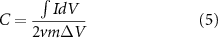
Standard image High-resolution imageThe microscopic morphology of M-IV composites is observed by transmission electron microscopy (TEM) at different views and sizes. Figure 5(a) shows the microstructure of M-IV at high magnification. The folded edges of the M-IV composite show a unique multilayer structure, the Ag NPs and Cu NPs are not only adsorbed on the surface and edges of V2CTx , but also most likely grow in the multiple interlayers. Figures 5(b) and (c) show the local enlargement, which show the ordered arrangement of Ag NPs and Cu NPs in the V2CTx , occupying most of its space. The Ag NPs and Cu NPs grow uniformly between the layers of V2CTx and act as supports to prevent the collapse of its two-dimensional structure, ensuring the normal transport of electrons and smooth diffusion of ions at the surface and interlayer of V2CTx . Ag NPs and Cu NPs effectively cover the surface of V2CTx due to the strong adsorption ability. Because of the orderly arrangement of Ag NPs and Cu NPs on the surface of V2CTx by passivation, the M-IV composite shows well structural stability. Figure 5(d) shows the microstructure of M-IV. The black shaded parts of the figure 5(d) are mostly composed of a large number of Ag NPs and Cu NPs grown on V2CTx , some of which enter the interlayer, effectively protecting the unique layered structure of V2CTx and ensuring the transport of electrons and electrolyte ions. Figure 5(e) shows the low magnification maps of M-IV at other location. It can be observed from the figure 5(b) that Ag NPs and Cu NPs occupy most of the structure of V2CTx , preventing its collapse while high conductivity Ag NPs and Cu NPs undergo agglomeration to form more conductive channels for rapid electron transfer. Figure 5(f) shows the V, O, Ag, and Cu elements in the M-IV composite. V is the main constituent element of the M-IV composites. The distribution of O is due to the abundance of oxygen-containing functional groups (–O, –OH) introduced into the structure of V2CTx during HF etching while Ag NPs and Cu NPs contribute to the oxidation of V2CTx . A lot of Cu2+ are attracted to the surface and interlayer of V2CTx and grow uniformly by electron exchange, and the Cu NPs also aggregate and combine with Ag NPs, forming the high rate conductive channel which is the basis for promoting excellent electrochemistry.
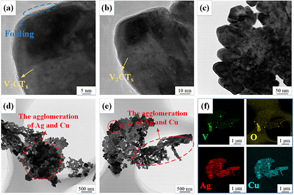
Figure 5. (a)–(e) The high magnification TEM image of M-IV at different angles and dimensions. (f) HR-EDS mapping images of M-IV.
Download figure:
Standard image High-resolution imageIn order to further investigate the changes in the functional groups on the surface of V2CTx caused by the formation of Ag NPs and Cu NPs, XPS analysis is performed on the M-II, M-III, and M-IV composites. Figure 6(a) shows the full spectra of M-II, M-III and M-IV composites. It can be seen from figure 6(a) that all the samples are composed of C, O, and V elements, while the Ag signals appear in the M-III indicating the successful formation of Ag NPs. The M-IV shows not only Ag signals but also Cu signals, indicating the successful entry of Cu NPs into the structure of V2CTx . The Ag NPs and Cu NPs enter into the interlayer of V2CTx , which act as supports to protect the layered structure. Figure 6(b) shows the XPS pattern of M-II. The high resolution V 2p spectrum can be deconvoluted into four components corresponding to V5+, V4+, V3+ and V2+/V-C, respectively. The peaks of V3+ are attributed to the loss of V during HF etching [43]. The C 1s spectrum can be deconvoluted into six components corresponding to C–V, C–C, C–O, C=O, O–C–O and –COOH, respectively. Due to the deposition of carbon on the surface or selective termination of V during etching [44], resulting in the formation of C–C bond. The binding of C and O is inextricably linked to the functional groups introduced on the surface of V2CTx and the oxidation reaction. The O 1s spectrum can be deconvoluted into three components corresponding to C=O, C–O–C and C–OH bonds, respectively. The F 1s spectrum can be deconvoluted into two components which locate at 684.4 eV and 688.9 eV corresponding to V-F and C-F, respectively. Figure 6(c) shows the XPS pattern of M-III. The transition from the low valence V2+ to the higher valence V4+ and V5+ in the V 2p pattern drives the transition from Ag+ to Ag NPs. The redox reaction occurring in the M-III promotes the transfer of electrons and ion movement. The change of the C–O bond in the C 1s spectrum is mainly due to the oxidation of V2CTx during the formation of Ag NPs and the decrease of the number of the oxygen-containing functional groups on the surface. The peaks of Ag 3d pattern locate at 368.08 eV and 374.08 eV corresponding to Ag 3d5/2 and Ag 3d3/2, respectively. The binding energy difference between the two is about 6 eV. Both the peaks are in the form of Ag(0) presenting in the M-III and no other valence state of Ag signal appears [17, 45], indicating that the lower valence state of V show the strong reducing effect. Figure 6(d) shows the XPS pattern of M-IV. It can be observed from V 2p that the area of the convolution peaks of V4+ and V5+ increases and the area of V2+ decreases sharply, which is due to the redox reaction during the formation of Cu NPs. The change of V2+ to V4+ and V5+ further promotes the formation of Cu NPs. The presence of Ag signals locate at 368.62 eV and 374.63 eV in the Ag 3d pattern indicates that the formation of Cu NPs does not diminish the presence of Ag NPs. The appearance of signals of Cu from the plot of Cu 2p with peaks locating at 932.73 eV and 952.49 eV [46], indicating that Cu NPs successfully enter into the structure of V2CTx . The presence of Cu as a metal monomer in M-IV is a mechanism similar to the reduction of Ag in the presence of the obtained V2CTx precursors. The growth of Ag NPs and Cu NPs in the V2CTx structure not only consumes a large number of functional groups that are detrimental to the electrical properties, but also enter the interlayer to protect the layered structure of V2CTx and ensure the normal movement of electrons and ions in the M-IV composite. Ag NPs and Cu NPs enter into the interlayer, increasing the layer spacing and promoting the exposure of its surface that possesses more active sites in the electrolyte, which promotes the movement of electrons and diffusion of ions on the surface. The mutual attraction and aggregation by Ag NPs and Cu NPs between the V2CTx layering form more and larger conductive channels, which shorten the electron transfer distance and improve the electron transfer efficiency.
Figure 6. (a) XPS survey spectra of the M-II, M-IⅡ and M-IV. (b) High resolution spectra of the M-II. (c) High resolution spectra of the M-ⅡI. (d) High resolution spectra of the M-IV.
Download figure:
Standard image High-resolution imageFigure 7 illustrates the physical growth model of the M-IV composite. Figure 7(a) shows the schematic structure of M-I, which is a three-dimensional dense-like structure composed of alternating metal V, Al and C elements. Figure 7(b) shows the schematic structure of M-II. The Al layer in V2AlC is removed by HF and transformed into V2CTx with higher surface activity, higher adsorption capacity and lower electron potential energy barriers. During the etching process, a large number of negatively charged functional groups are introduced on the surface of V2CTx which cause the deterioration of the electrochemical properties. Figure 7(c) shows the structural diagram of M-III. When AgNO3 solution is added, the positively charged Ag+ exchanges electrons with the negatively charged functional groups, and lots of Ag+ are reduced to Ag NPs, consuming the functional groups on the surface of V2CTx . The Ag NPs enter the interlayer of V2CTx as the support to protect its unique layered structure and increase the layer spacing, resulting in a larger surface area with rich active sites, providing more vacancy binding sites for Cu NPs growth. Figure 7(d) shows the structural diagram of M-IV. The reduction of Cu2+ into Cu NPs consumes the functional groups on the surface of V2CTx and improves electrochemical properties. Cu NPs enter the interlayer of V2CTx to protect its layered structure from collapse and ensure the normal transport of electrolyte ions and electrons. The growth of Cu NPs promotes the formation of Ag NPs, which grows uniformly at the edges of V2CTx layering. The combination of Ag NPs and Cu NPs forms a conductive channel covering multiple layers, which realizes the fast electron transfer between multiple V2CTx , reduces the electron transfer distance and improves the electron transfer efficiency. The growth of Ag NPs and Cu NPs causes the layered structure of M-IV more open, which exposes more active sites on the surface of V2CTx and promotes the diffusion behavior of ions and electron transfer in the electrolyte solution.
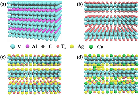
Figure 7. The physical growth model of M-IV composite.
Download figure:
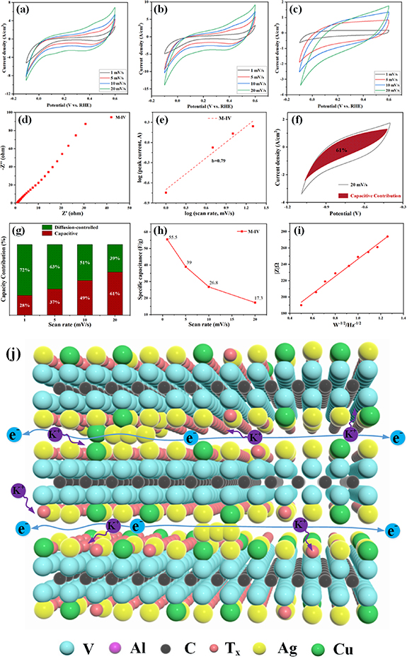
Standard image High-resolution imageThe electrochemical performance of the M-II, M-ⅡI and M-IV composites are further investigated using a three-electrode system, in which the hybrid fiber is used as the working electrode, the counter electrode is platinum wire and Ag/AgCl is used as the reference electrode. The electrolyte solution is 6 M KOH solution. The cyclic voltammeter curves shows that the M-II, M-III and M-IV composites can work stably under the potential window of −1.1 to −0.4 V. Figures 8(a) and (b) shows the CV curves of M-II and at the scan rates of 1 mV s−1, 5 mV s−1, 10 mV s−1 and 20 mV s−1. The small broad peak appears in the CV curve of M-II [47], which is related to the continuous change of V valence state during redox. As shown in figure 8(b), as the voltage scan rate increases, there is no significant distortion in the shape of the CV curve, indicating its favorable multiplicative performance. Figure 8(c) shows the CV curves of M-IV at different scan rates, showing the same trend as M-II and M-III. There is no prominent peak in the CV curve of M-IV, indicating that the redox reaction occurs at a constant rate throughout the cycle. The CV curves show outstanding centrosymmetry, indicating that M-IV still shows good cycle reversibility at high scan rates.
Figure 8. CV curves of (a) M-II, (b) M-ⅡI and (c) M-IV at 1, 5, 10 and 20 mV s−1 scan rates. (d) EIS of M-IV. (e) Relationship between log (i) and log (v). (f) The M-IV of pseudo-capacitance contribution at 20 mV s−1 (g) Pseudo-capacitance contribution at different scan rates. (h) Specific capacitance as a function of the scan rate for M-IV. (i) Extracted |Z| vs. ω1/2 plot for M-IV composites in the low frequency region. (j) The schematic diagram of the electron transfer within the M-IV electrode.
Download figure:
Standard image High-resolution image
To further investigate the internal resistance, charge transfer kinetics and ion diffusion processes of the electrode materials of M-IV, the Nyquist plot of the M-IV electrode is shown in figure 8(d). The tested Rs value of M-IV is 0.72 Ω, which shows a relatively low intrinsic resistance, indicating an excellent electrical conductivity. It shows that the conductive channel constructed from Ag NPs and Cu NPs significantly reduces its internal resistance. When electrons are transferred from the conductive channels formed by the lamellar edges of V2CTx , the electrons can be transferred rapidly between the layers due to the outstanding conductivity of Ag NPs and Cu NPs, effectively reducing the resistance of electrons during the transfer process. The M-IV electrode shows a straight line with a higher slope in the low frequency region [48], indicating that ion migration becomes easier, which is related to the increase of active sites with the increase of layer spacing. The relationship between the peak current (i) and the sweep speed of (v) is obtained according to the equations (1) and (2) as shown in figure 8(e). When the b = 0.5, the electrode charge storage is completely controlled by the diffusion process. When the b = 1, the charge storage is completely controlled by the surface capacitance effect. The value of M-IV electrode is about 0.79, which indicates that its charge storage is controlled by both diffusion and surface capacitance effect, and the diffusion process originates from the difficulty of electrolyte ions to enter the deeper ion adsorption sites between the layers of V2CTx .
Figures 8(f) and (g) show the quantitative effects of surface capacitance effects and ion diffusion control processes on the total current. The contribution of M-IV surface capacitive effect to the total current is 61% at a sweep rate of 20 mV s−1, which is obtained by equations (3) and (4). As shown in figure 8(f), the contribution of the capacitive effect to the total current of M-IV at low and high potentials is 28% and 61%, respectively. It indicates that the lower contribution of its capacitive effect to the total current is due to the charge storage at high potentials is mainly controlled by diffusion, which is consistent with the b-value calculation. Figure 8(h) shows the specific capacitance of the M-IV electrode of the CV curve which is obtained according to equation (5). The results show that the specific capacitance decreases from 55.5 F g−1 to 17.3 F g−1 as the scanning speed increases from 1 mV s−1 to 20 mV s−1, respectively. Figure 8(i) shows the relationship between Z' and ω−1/2 (ω = 2πf) in the M-IV electrode. The slope of the M-IV electrode in the low frequency region is 105, indicating that the M-IV electrode material shows an excellent diffusion capacity of K+. The reason is that the number of layers of V2CTx are denser at the beginning of the test, and the electrolyte ion diffusion path is long. As the test continues with ion insertion and detachment, the layer structure is gradually opened, allowing rapid electrolyte ion transfer.
Figure 8(j) shows the schematic diagram of the electron transfer path of the M-IV electrode material. V2CTx shows the advantages of excellent electrical conductivity, large surface area, low electron and ion diffusion barriers. On the basis of V2CTx , Ag NPs and Cu NPs with outstanding electrical conductivity are introduced into the interlayer as supports to protect the lamellar structure from accumulation, and also to ensure the smooth penetration of K+ and normal electron transport between the layers of V2CTx . The Ag NPs and Cu NPs effectively reduce the effect of terminated functional groups on the surface of V2CTx and thus improve the electrochemical properties. In addition, Ag NPs and Cu NPs aggregate at the lamellar edges of V2CTx , forming a conductive network covering multiple layers, which shortens the electron transfer path and realizes rapid electron transfer across layers. The formation of the conductive network facilitates the rapid transfer of electrons on the surface of V2CTx and between the layers as well as the transport of electrons between individual V2CTx . Meanwhile, Ag NPs and Cu NPs enter the interlayer to expand the interlayer spacing, exposing more active sites on the surface of V2CTx , creating a green channel for electron transport and K+ diffusion. The M-IV composite as an electrode show excellent conductivity, low ion and electron permeation barriers and abundant surface functional groups favorable to K+ adsorption/insertion, while the multiple oxidation states of vanadium allow V2CTx to participate in multi-electron redox reactions. The M-IV composites as electrons show great potential for electrochemical energy storage applications.
4. Conclusion
In summary, the V2CTx /Ag/Cu composite is prepared by a simple and efficient solution mixing method and by the self-reduction process of V2CTx . The Ag NPs and Cu NPs are introduced on the basis of V2CTx , which possesses high electrical conductivity and low electron permeation barriers, reducing the internal resistance of the material and improving the ion and electron transfer efficiency. The uniform growth of Ag NPs and Cu NPs at the layered edge of V2CTx protects its layered structure ensuring the transfer of electrolyte ions and electrons between the layers. Moreover, the increase of layer spacing of V2CTx resulting in the formation of more active sites on the surface, which accelerating the diffusion and permeation efficiency of electrolyte ions. According to the electrochemical performance tests, it can be seen that the internal resistance of V2CTx /Ag/Cu composite is only 0.72 Ω, which shows a low internal resistance. The shape of its CV curve does not deform significantly with the increase of voltage sweep rate, which shows a stable electrochemical performance. These results suggest that agglomeration of Ag NPs and Cu NPs at the delamination edge of V2CTx occurs, forming conductive channels that can cover multiple interlayers. These conductive channels can assist electron transfer across the layers, reducing the resistance to transfer and improving the electron transport efficiency. Meanwhile, the Ag NPs and Cu NPs entering the V2CTx interlayer increases the layer spacing, and the more open layered structure leads to the generation of more active sites, which improves the ion transfer and storage capacity of V2CTx /Ag/Cu composites.
Acknowledgments
This project is supported by the National Natural Science Foundation of China (Grant No. 5210040951).
Data availability statement
The data that support the findings of this study are available upon reasonable request from the authors.
Declaration of competing interest
All authors of this manuscript have directly participated in planning, execution, and/or analysis of this study. The contents of this manuscript have not been copyrighted or published previously. The contents of this manuscript are not now under consideration for publication elsewhere. The contents of this manuscript will not be copyrighted, submitted, or published elsewhere. There are no directly related manuscripts or abstracts, published or unpublished, by any authors of this manuscript.
Conflict of interest
There are no conflicts to declare.