

Abstract
The twistronics of the atomic-thick two-dimensional (2D) van der Waals materials has opened a new venue to investigate the interlayer coupling. Till now, most studies focus on the twist of atomic lattices and the resulted moiré superstructures, while the reports about the twist of charge density waves (CDWs), the superstructures of which are from individual layers are limited. Here, using molecular beam epitaxy, we construct bilayer (BL) 1T-NbSe2 vertical structures. With high resolution scanning tunneling microscopy observations, we identify two cases of CDW twisted stacking with atomic precision. The typical twist angles are 0° and 60° between the 1st and the 2nd layer, although the top Se atomic lattices of these two layers are parallel. Compared to the single layer case, the dI/dV at BL shows an insulator-to-metal transition, with the Hubbard bands shrinking towards the Fermi level (EF). More intriguingly, interlayer coupling states rise near EF, which are related to the CDW twist angles. These findings give fresh insight into the engineering of 2D materials by CDW twisting and are potentially applicable for future nanoelectronic devices.
Export citation and abstract BibTeX RIS
1. Introduction
The recent exploration of the twisted bilayer (BL) two-dimensional (2D) system was initiated in graphene [1–4] and soon extend to TMDC [5–7] and other 2D materials [8–10]. The twisted 2D system leads to various intriguing properties, such as unconventional superconductivity [2, 11], Mott insulator and flat bands [1, 4], Hofstadter's butterfly spectra [12, 13], moiré excitons [14–16], piezoelectric networks [17], quasicrystalline [18] and thus open a new research area known as twistronics [19–21].
Most of the previous works on twistronics focused on the twist of atomic lattice following with moiré patterns [22, 23]. However, the reports about twist of charge density waves (CDW) patterns are quite limited. As a typical collective electronic behavior, CDW is quite important in both fundamental understanding of low-dimensional quantum materials and potential application in ultrafast switches and memories [24, 25]. Meanwhile, the interlayer coupling plays a critical role in engineering the electronic properties by quantum confinement and vdW interaction in 2D materials [26–29]. Although there are some works about the twist [30, 31] or stacking fault [32] of CDW in bulk systems, a study on the atomically well-defined CDW twisted superstructures and corresponding interlayer coupling electronic states is still lacking.
Here, we report a new kind of twisted structure: BL 1T-NbSe2 with different CDW twist angles (0° and 60°). The scanning tunneling microscopy (STM) investigation reveals the twist of CDW patterns can not only determine the alignment of the long and short edges of the 1st and 2nd layers, but also determine the rotation angle of the 1T atomic lattice of these two layers. Moreover, it is found that at BL, the Hubbard bands move towards the Fermi level (EF) compared to single layer (SL) one, and there is an insulator-to-metal transition (IMT) due to the interlayer coupling states (ICS), which are strongly dependent on the CDW twist angles. Thus our 'CDW twisted' vertical junction has opened a novel and versatile venue for the tailoring of the emerging 2D materials-based nanoelectronic devices.
2. Methods
2.1. Sample preparation and STM measurements
Molecular beam epitaxy (MBE) and STM experiments were performed in a Unisoku UHV system (base pressure 1 × 10⁻¹⁰ mbar) comprising MBE chambers and a low-temperature STM chamber. BL graphene (BLG) was grown by the thermal decomposition of 4H–SiC (0001) at 1200 °C for 60 min. NbSe2 islands were prepared by the MBE method at a deposition rate of ∼0.002 ML min−1. An elemental Nb rod was used as the metal source in the e-beam evaporators (Focus Ltd.), whereas an elemental Se source in a Knudsen cell was heated to 120 °C. The deposition ratio of Se to Nb was larger than 30:1. During film deposition, the background pressure in the chamber was ∼3.0 × 10⁻⁹ mbar. The BLG/SiC substrate was kept at ∼550 °C during the deposition and post-annealing process to improve the diffusion and desorb excess Se. STM imaging was performed using mechanically cut PtIr tips at a liquid helium temperature (4.2 K). The dI/dV tunneling spectra were acquired using lock-in detection by applying an AC modulation of 10 mV (rms) at 973 Hz to the bias voltage.
3. Results and discussion
Whereas the bulk 1T-NbSe2 is unstable and does not exist [33], SL 1T-NbSe2 (which contains three atomic layers) can be prepared on BLG/SiC surface by MBE method [34, 35], providing an ideal platform to study the intriguing relationship between strong correlated electronic states and Star of David (SOD) CDW superlattice [36]. As seen in the upper panel of figure 1(a), the SOD cluster includes 13 Nb atoms at three different equivalent sites in the middle plane, six Se atoms in the top plane, and six ones in the bottom plane. The six topmost Se atoms contributed more to the electron tunneling and resulted in the triangular shape in STM imaging, as illustrated in the middle plane of figure 1(a). By CDW twist of 60° from figures 1(a) to (b), the side views show the three-layer atomic lattice configuration also change from α to β (laterally flipped). Thus, the rotation of the 'imaged triangular SOD' shape serves as a handy indicator for determining the three-layer atomic lattice orientation.

Figure 1. Two types of BL 1T-NbSe2 islands with CDW twist angles of 0° and 60°. (a) (upper panel) SOD model of 1T-NbSe2. In STM imaging one SOD appears as a triangle, because the top six Se atoms contribute more. The middle and bottom panels illustrate the three atomic-layer ball-and-stick model of the area around the SOD. (b) Similar with (a) but twisted by 60°, and the side view configuration changed from α to β (c), (d) STM images of BL 1T-NbSe2 islands, with the longer edge (indicated by white dashed lines) of the 1st and 2nd hexagonal layer twisted by 0° and 60°, respectively. (e), (f) Zoomed-in images of the area in the rectangular frame in (c) and (d), respectively. The SOD clusters in the 1st layer are labeled by grey triangles, and the SOD clusters in the 2nd layer are labeled by green and blue triangles for 0° and 60° twisted cases compared to the 1st layer one, respectively. Scanning parameters: (c)–(f), bias voltage VB = −1.5 V, tunneling current It = 20 pA.
Download figure:
Standard image High-resolution imageFigures 1(c) and (d) show the large-scale STM images of typical 1st/2nd layer islands. The 2nd layer 1T islands are always smaller than the 1st layer one, forming a wedding-cake structure. The 1st and 2nd islands both have the truncated triangle shape, with the alternative longer and shorter edges indicated by the white and black dashed lines, respectively. The adjacent edges from the 1st and 2nd layer are parallel, indicating the top Se atom lattice are parallel. According to the twist angle of the longer edges between the 1st and 2nd layer, these islands can be classified into two cases: twist of 0° and 60°, as shown in figures 1(c) and (d), respectively.
To get the CDW information of these two twist cases, we further zoom in the rectangular areas, as seen in figures 1(e) and (f). Both the 1st and 2nd layers show a similar array of triangular shape SOD. The unit cells of SOD in the 1st and 2nd layers for both cases are represented by the rhombuses, and arrows running along the long diagonal of the rhombus are defined as the orientations of the CDW pattern. Whereas the CDW twist between the 1st/2nd layer is 0° for figure 1(e), the twist is 60° for figure 1(f). Comparing figures 1(c)–(e) (twist 0° case), it is interesting to note that the imaged triangular shape of SOD mimics the macroscopic truncated triangular island shape, and this rule also holds for twist 60° case (figures 1(d)–(f)), as summarized from tens of BL 1T islands. Thus these two cases are named as 0° and 60° islands, with the angles referring to twist of the triangular shape SOD CDW as well as the longer edge of the 1st and 2nd layers.
Note that the system is three-fold symmetric, so the 60° twisted one can be also regarded as an antiparallel one (60° + 120° = 180°). If we consider the three-atomic-layer structure of 1T, the Se atoms bonding configurations with the central Nb are in the opposite direction for the 0° and 60° cases. Normally 1T means the unit cell is just one layer, different from 2H which has two layers as the vertical period. As seen in the schematic side views in figures 1(e) and (f), here we have found two different types of BL 1T twist angles, and redefine the T phase unit-cell in the vertical direction as 2Ta (α on top of α configuration), 2Tb (β on top of α configuration). The ratio of these two CDW twists is 22:30, counted from tens of BL 1T islands. We take advantage of the 'imaged triangular shape' of the SOD to identify the CDW twist and determine the three-layer atomic 1T structure.
To get the stacking relationship of the 1st and 2nd layer precisely, we have obtained the atomic resolution images (current channel) across the 1st and 2nd layers near the step edge as shown in figure 2 (for the height channel, see figure S1, supplementary information available online at stacks.iop.org/2DM/9/014007/mmedia). The procedure to determine the relative position of the two layers is as follows: (a) overlay the green circle array onto each of the central Nb (commonly named as Nb1) of SOD at the 1st layer; (b) extrapolate the array to the area of the 2nd layer; (c) compare the positions of the green circles with the position of Se atoms in the 2nd layer. Figure 2(a) shows that Nb1 of the 1st layer is underneath the outmost Nb of the SOD at the 2nd layer. The relative CDW lattice shift can be projected onto the SOD model, as shown in figure 2(b). While for the 60° case, the most common stacking is shown in figure 2(c). The Nb1 in the 1st layer is right below a corner of the six Se-atom 'imaged triangle' within the SOD at the 2nd layer. The relative CDW lattice shift can be projected onto the SOD model, as shown in figure 2(d), which is different from the 0° case. With the atomic resolution of both the 1st and 2nd layers, it is easy to pinpoint the exact stacking order accurately.
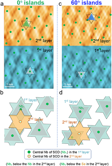
Figure 2. Atomic characterization of the two types of CDW twist. (a) STM image (current channel) of the 2nd layer 1T-NbSe2 on top of the 1st layer island with CDW twist of 0°. The green circle represents the central Nb atom of the SOD at the 1st layer, which is underneath the outmost Nb of the SOD at the 2nd layer. The relative CDW lattice shift can be projected onto SOD clusters of the 1st and 2nd layer, as shown in (b). (c) STM current image for the BL-1T NbSe2 with CDW twist of 60°, showing that the central Nb of the 1st layer is underneath the outmost Se atom in the 'imaged triangle' within the SOD at the 2nd layer. (d) The relative CDW lattice shift derived from the atomic resolution image in (c) for CDW twist of 60°. Scanning parameters: (a) −1.3 V, 5 nA, (c) −1.5 V, 1 nA.
Download figure:
Standard image High-resolution imageThe Nb1 in SOD is important in that the other 12 Nb atoms contract towards it, leaving the only unpaired dz2 orbital with spin = 1/2 at this site [36, 37], similar to the situation in TaS2 [38]. The vertical extension of the orbital will influence the interaction between neighboring Nb1 dz2 orbitals in the 1st and 2nd layers [39–42], and modulate the electronic structures. Before investigating the possible influence of twisted angles on the electronic structures, we first performed the dI/dV spectroscopy on the 0° twisted CDW BL case (figure 3), where new peaks appeared by the comparison with the SL case. Such new peaks are related to the interlayer coupling states (ICS). Then we illustrated the existence of the ICS in 0° and 60° twisted CDW BL cases (figure 4).
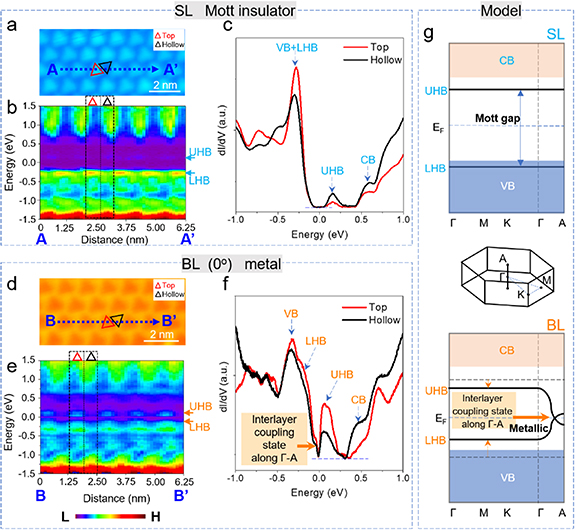
Figure 3. IMT with interlayer coupling state. (a) and (d) STM images of SL and BL 1T-NbSe2 (with 0° CDW twist angle), respectively. AA' and BB' are the lines along which the line dI/dV spectra in (b) and (e) are obtained, respectively. (b) and (e) Line dI/dV spectra along several CDW SOD periods. (c) and (f) Averaged point spectra of the top and hollow sites of the SL and BL (labeled by the red and black triangle in figures (b)–(e)), respectively. (g) Upper panel and bottom panel: the shrinking of the UHB-LHB gap and the appearance of the ICS from SL to BL; middle panel: the unit cell of the reciprocal space containing high symmetry points. The scanning and spectroscopy parameters: (a) and (d) −1.5 V, 10 pA; (b), (c), (e) and (f) −1.5 V, 1 nA before turning off the feedback loop.
Download figure:
Standard image High-resolution image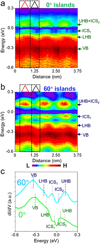
Figure 4. CDW-twist-dependent ICS. (a) and (b) Line dI/dV spectra across three SOD periods for the two types of CDW twist, showing the different intensities of ICS. The top and hollow sites are labeled by the red and black triangles. (c) Averaged point spectra of the top sites of the 2nd layer with CDW twist of 0° and 60°. The spectroscopy parameters: (a), (b) and (c) −1.5 V, 1 nA before turning off feedback loop.
Download figure:
Standard image High-resolution image
Figures 3(b)–(e) show the line dI/dV spectra across several SOD clusters of the SL and BL 1T-NbSe2 (0° CDW twist case, for the 60° CDW twist case, see figure S2, supplementary information), respectively. The paths are along AA' in figure 3(a) and BB' in figure 3(d), top and hollow sites are indicated by the red and black triangles, both with the periodic feature. However, one evident difference is that near the EF the line dI/dV spectra reveal the insulator and metallic feature for the SL to BL, respectively. In other words, there is an IMT from the SL to BL.
The averaged point spectra of the SL and BL are shown in figures 3(c)–(f). As we have demonstrated in the previous work [36], the SL 1T-NbSe2 is a Mott insulator with the upper Hubbard band (UHB) at +0.17 eV, and the lower Hubbard band (LHB) hybridized with valence band (VB) forming a broad peak at −0.28 eV. At the BL region, pronounced peaks appear at −0.31 eV and +0.11 eV. In addition, there is a shoulder appearing at −0.15 eV next to the −0.31 eV peak, which corresponds to a splitting of LHB and VB. For increasing layer, it is a general phenomenon that the LHB and UHB move towards the EF due to increased screening of the additional layer of material compared to the vacuum [43, 44], whereas the VB and conductance band (CB) are less affected. Thus, the shoulder at −0.15 eV, which moves closer to EF is attributed as the LHB, and the peak at −0.31 eV is assigned to the VB. This attribution also works for the unoccupied states: the UHB moves towards EF, from 0.17 eV at SL to 0.11 eV at the BL, whereas the CB for BL is at an energy position around +0.5 eV.
Besides the shrinking of the Mott gap for the BL, there is a weak shoulder at ∼ −40 meV which lies between the UHB and LHB. It is absent in the SL, and should be attributed to the ICS rising from the stacking. According to the previous DFT calculations of TaS2, the IMT behavior from SL to bulk is ascribed to the interplane dispersion [45], i.e. the 1D band along the vertical (Γ–A) direction (figure 3(g)). This state always lies between LHB and UHB, thus we can safely attribute the weak shoulder or peak at −40 mV to the ICS. The ICS also appears at the unoccupied states near the EF, as it overlaps with the UHB, so the state at ∼0.11 eV is enhanced compared to the SL case. Thus from SL to BL, there is a shrinking of the UHB–LHB gap and the appearance of the ICS, as schematically illustrated in figure 3(g). The middle panel in figure 3(g) shows the unit cell of the reciprocal space containing high symmetry points.
To investigate if the electronic structure can be modulated by the different CDW twisting, we have performed the line dI/dV spectra along several SOD clusters for the two twist cases, as shown in figures 4(a) and (b). It is seen that the line dI/dV spectra both have periodic spatial distribution with the SOD clusters. Both of them have a broad peak centered around −0.33 eV. The dI/dV spectra in figure 4(c), taken at the top sites for the two twist cases, show the ICS more clearly. Two ICS are identified, which rise from the dispersion of both occupied and unoccupied states along the Γ–A direction and are named ICS1 and ICS2. One distinction between the two cases is the intensity of the ICS1 and ICS2. For the 0° case, the ICS2 is quite enhanced and merges with the UHB, while for the 60° case the ICS1 is significantly enhanced and appears as an individual peak. This is not surprising since the 0° and 60° cases have different orbital stacking relationships as known from figure 2.
Besides, the CDW twist also induces energy peak position shift, as seen in the statistical analysis summarized in table 1. There exists clear shift for the peak of ICS1, with the shift from −36 mV for 0° case to −70 mV for 60° case. In contrast, the VB and CB are less affected since they originate more from the individual layer structure. This trend can be seen more clearly from the relative changes of the peak positions (the last row in table 1), which show the ICS1 and ICS2 (bold in table 1) have a relative change of 94% and 20%, respectively, while for other peaks the values are reduced to 4% ∼ 11%. This difference shows the ICS are more influenced by the CDW twist, which results in different d orbital stacking, especially from Nb1 (figure 2).
Table 1. The average energy position of the bands near EF, depending on the CDW twist angles. The averaged value and error bar of the peak positions are obtained by fitting with Gaussian distribution, as shown in figure S3, supplementary information. The shift of peak positions and the relative shift ratio are also listed.
| Energy position (meV) | ||||||
|---|---|---|---|---|---|---|
| Twist angle | VB | LHB | ICS1 | ICS2 | UHB | CB |
| E1 for 0° | −319 ± 9 | −165 ± 17 | −36 ± 3 | 51 ± 3 | 111 ± 7 | 429 ± 17 |
| E2 for 60° | −334 ± 9 | −183 ± 8 | −70 ± 2 | 41 ± 6 | 118 ± 9 | 447 ± 43 |
| |E1 − E2| | 15 | 18 | 34 | 10 | 7 | 18 |
| |E1 − E2|/E1 | 0.04 | 0.11 | 0.94 | 0.20 | 0.06 | 0.04 |
4. Conclusions
In conclusion, using high-resolution STM on the CDW twisted BL 1T NbSe2, we identified two twist angles of 0° and 60°. The CDW twist has an obvious influence on the electronic band structures, especially on the interlayer coupling state. In addition, there is an IMT transition from SL to BL, with a shrinking UHB–LHB Mott gap. Our CDW twisted systems provide nice platforms to tune the electronic structures near the Fermi level via the CDW twisted stacking, and are potentially applicable for future nanoelectronic devices.
Acknowledgments
Thanks for the financial support from National Key Research and Development Program of China (2020YFA0308800, 2019YFA0308000, 2021YFA1400100), National Natural Science Foundation of China (Nos. 61971035, 61725107, 92163206), Beijing Natural Science Foundation (Nos. Z190006, 4192054).
Data availability statement
The data that support the findings of this study are available upon reasonable request from the authors.