

Abstract
Defects in hexagonal boron nitride (hBN) have attracted much attention since they are effectively used for nanoelectronics, such as single-photon emitters or memristors. The method for generating and controlling hBN defects is important because the defects are critical factors determining the optical and electrical properties of hBN. Here, we demonstrate the modulation of optical and electrical properties of hBN by defects generated via mild oxygen plasma treatment. The photoluminescence peaks related to defects were observed at a broad range (∼3.8 eV), and the current of plasma-treated hBN flow at the lower threshold voltage compared to the as-exfoliated hBN due to the formation of defect paths inside the hBN structure. We also demonstrate that the bandgap structure of hBN can be tuned by the oxygen plasma treatment. Our findings are useful for the stable and reliable fabrication of two-dimensional electronic devices using hBN in the future.
Export citation and abstract BibTeX RIS
1. Introduction
Hexagonal boron nitride (hBN), a two-dimensional (2D) insulating material with a wide band gap (5.5–6.0 eV) has drawn much attention as used for the ideal insulating substrate and tunnel barrier for 2D materials transistor that are benefited by the absence of dangling bond, high crystalline quality, and thermal stability [1–5]. Recently, defects of hBN have been used for electrical and optical devices, such as single photon emitters and memristors [6–9]. Many studies have been conducted to characterize the devices employing hBN defects and induce them by various methods, such as laser ablation [10, 11], ion/electron irradiation [12], and chemical etching [13]. However, little attention has been paid to the study on the modulation of optical and electrical properties of hBN induced by defects in spite of the large effect of defects in the performance of 2D heterostructure devices. Here, we investigate how the plasma-induced defects of hBN modulate its intrinsic optical and electrical properties. The oxygen plasma treatment generates the oxygen-related defects in the crystal structure of hBN, which lead to the increased photoluminescence (PL) intensity depending on the energy levels and amounts of defects within the large band gap of hBN. The insulating barrier of plasma-treated hBN decreases significantly due to the defect-induced conductive paths. In addition, photoemission spectroscopy (PES) measurement exhibits a bandgap narrowing due to the disordered structure of plasma-treated hBN.
2. Method
2.1. Sample preparation
The hBN flakes were mechanically exfoliated on the 285 nm thick SiO2/Si substrates. Oxygen plasma treatment was carried out on the hBN flake using a reactive ion etch (RIE) mode (Femto Science, CUTE). The treatment parameters are as follows: RIE power (100 W), frequency (100 kHz), pressure (10−1 Torr), O2 flow rate (20 sccm), and treatment time (1–31 s). The as-exfoliated and plasma-treated hBNs were transferred onto Au-coated SiO2 substrates for the conductive atomic force microscopy (c-AFM), Kelvin probe force microscopy (KPFM), PES, and near-edge x-ray absorption fine structure (NEXAFS) measurements.
2.2. Material characterization
The as-exfoliated and plasma-treated hBNs were examined by Raman spectroscopy with a 325 nm He-Cd laser (Horribar Jovin Yvon, LabRAM ARAMIS). The AFM (Park System, NX-10) was used to measure the friction force microscopy (FFM), c-AFM and KPFM in ambient conditions. For contact modes (FFM and c-AFM) and non-contact mode (KPFM), a soft-tip coated by Pt (Nanosensor, PPP-CONTSCPT) was used under the fixed loading force of ∼3 nN. For the c-AFM measurements, a specimen was mounted on a metallic sample holder, and an external current amplifier (FEMTO, DLPCA-200) was used to measure the extremely low current. The cross-section transmission electron microscopy (TEM) and electron energy loss spectroscopy (EELS) analysis was conducted using a Cs-corrected TEM (JEOL, JEM-ARM200F) at 80 kV. PES and NEXAFS spectra were measured at 4D and 8 A beam line at Pohang Accelerator Laboratory. The NEXAFS spectra were obtained with partial electron yield at a 45° angle of the incident beam with respect to the surface of the samples.
2.3. Computational method
To comprehend the PL, we performed the first-principles calculations based on density functional theory (DFT). We used a hexagonal unit cell, which is 8 × 8 × 1 supercell of the primitive unit cell of hBN. The lattice constant in the in-plane direction is 20.08 Å, and the vacuum between two planes is 10 Å. All the calculations are performed using the Vienna Ab initio Simulation Package [14] with Perdew–Burke–Ernzerhof [15] functional to optimize the geometric structures and the screened hybrid HSE06 functional to obtain the more accurate energy gaps between two defect states. The valence electrons were spanned by the plane-wave basis with the cut-off energy of 500 eV, and the projector augmented wave potentials were employed [16, 17]. The Brillouin-zone was sampled only by the Γ-point and the positions of atoms are optimized with a force tolerance of 0.01 eV Å−1.
3. Results and discussion
3.1. Structure of plasma-treated hBN
The hBN flakes were mechanically exfoliated with a scotch tape on a SiO2 (285 nm)/Si substrate. The conventional plasma tools operating at high frequency vigorously etch ultrathin 2D materials, which are too harsh to generate a small number of defects [18]. We used customized plasma equipment to gently generate defects of low density on the hBN surface [19]. Our plasma system (pressure = 0.1 ∼ 1 Torr and adjustable working frequency = 100 kHz) enables us to precisely control the defect concentration of hBN due to minimized ion bombardment. To investigate the structural change of plasma-treated hBN, we used Raman spectroscopy with a high-energy laser of 325 nm wave length. Figure 1(a) displays the Raman spectra of plasma-treated hBN for different duration. The characteristic peak of hBN was observed at 1366 cm−1, which corresponding to the E2g phonon mode [20]. There was no recognizable change in position and full-width-at-half-maximum (FWHM) of the Raman peak even after plasma treatment for 31 s as shown in figure 1(b). The thickness and surface roughness of the plasma-treated hBN were measured by AFM in figure 1(c). The thickness of the hBN was reduced by 0.4 nm after the oxygen plasma treatment of 14 s, corresponding to etching rate of 1.7 nm min−1. The roughnesses of both as-exfoliated and plasma-treated hBNs showed a comparable value of ∼0.3 nm. To measure the friction of the plasma-treated hBN, we used FFM. Friction measurements of as-exfoliated and plasma-treated hBN in figure S1 (available online at stacks.iop.org/2DM/8/045041/mmedia) show that the friction increased right after the oxygen plasma treatment regardless of treatment time due to the B–N bond breaking and oxygen chemisorption on the surface of hBN [21]. The longer plasma treatment showed no increase in friction. Even though there is no recognizable change in Raman spectrum of plasma-treated hBN, there is clear change in the friction. This result implies that our plasma treatment induces a small number of defects in hBN. However, to verify the type and position of defects in hBN, we conducted further investigations as follows.
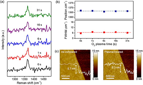
Figure 1. (a) Raman spectra of exfoliated hBNs before and after oxygen plasma time from 1 s to 31 s. (b) Variation of Raman peak position and full-width-at-half-maximum (FWHM) as a function of plasma time. (c) Topography of as-exfoliated and plasma-treated hBNs (white line shows the height profile before and after plasma treatment).
Download figure:
Standard image High-resolution image3.2. PL from the midgap energy states
To investigate the defects-induced energy states, PL spectra of hBN after the oxygen plasma treatment were acquired using a laser of 325 nm wave length as shown in figure 2(a). As the plasma treatment time increased, PL peaks emerged at 1.8, 2.3, 2.5 and 3.5 eV and gradually increased. To confirm the type of the defects responsible for the PL peaks, we performed the first-principles calculations based on the DFT. Figure 2(b) shows the structures of various defects, such as O substitution for nitrogen (ON), B vacancy (VB), B vacancy and ON (VBON), B vacancy saturated with two oxygen atoms (VBO2), and N vacancy (VN) and their in-gap states calculated by using a hybrid functional HSE06. We listed possible transition energy values, which are corresponding to the PL peaks. The first PL peak at 1.8 eV is associated with transition energy between the in-gap state of ON and the conduction band. The other three PL peaks at 2.3, 2.5 and 3.5 eV are comparable to the transition energies calculated from VB, VBON/VN, and VBO2, respectively. Therefore, the emerged PL peaks in the plasma-treated hBN are ascribed to the transitions within the midgap energy states of the defects. In order to generate the more defect-induced energy states, we measured PL spectra with longer oxygen plasma treatment time up to 76 s. As shown in the figure 2(c), PL intensity originated from the defects increases and is saturated around 30 s. This indicates that, as the hBN is etched simultaneously, total number of defects is maintained. Therefore, it is estimated that the band gap is constant after plasma treatment of 30 s.
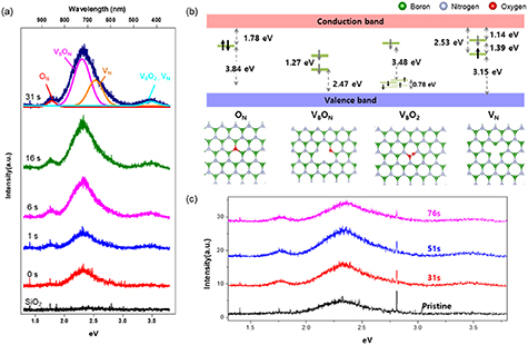
Figure 2. (a) Photoluminescence (PL) spectra of the hBNs before and after oxygen treatment time from 1 s to 31 s. The PL peaks increased with the plasma treatment time. (b) Top view of the five defect structures ON, VB, VBON, VBO2 and VN, and in-gap states calculated by using a hybrid functional HSE06. Black (gray) arrows indicate spin up and down at occupied (empty) states. (c) PL spectra of the plasma treated hBN for different time. The PL intensity originated from the defects increases and is saturated around 30 s.
Download figure:
Standard image High-resolution imagePES was measured to investigate the surface chemical composition of the oxygen plasma-treated hBN at hν = 750 eV. For the as-exfoliated hBN, figure 3(a) shows the main peak of B 1s and N 1s of core-level spectra that are located at 190.8 eV and 398 eV, respectively, which are in agreement with the previous reports of B–N bonding [22–25]. However, no O 1s peak was observed for the as-exfoliated hBN. After the oxygen plasma treatment of 14 s, the main peak intensities of B 1s and N 1s decreased dramatically along with the increased peak width as shown in figure 3(b). Unless noted otherwise, all samples used for analyses were treated by oxygen plasma for 14 s. The PES spectra were deconvoluted by using Gaussian fitting to extract the component peaks. The component peaks at 191.4 and 192.5 eV of the B 1s and 399.5 and 400.6 eV of the N 1s correspond to the BNx Oy , B–O, BNx Oy and N–O bonds, spectrum consisting of three component peaks emerged at 531, 533 and 534 eV after plasma treatment of 14 s, which indicates that O–B–N complexes are generated [26]. From the PES results, it can be noted that the ionized oxygen breaks B–N bonds and induces various defects such as VB,VN and oxygen-related bonds in the plasma-treated hBN. Figure S2 shows the relative atomic ratio obtained by calculating the area of the PES peaks (the area of N is normalized to 1) before and after plasma treatments for 14 s. While the as-exfoliated hBN reveals boron-rich condition, the relative atomic ratio of boron decreased from 1.27 to 0.59 after plasma treatment. It means that boron is more susceptible to oxygen plasma compared to nitrogen. Although the previous theoretical studies have reported that the formation energy of VB is higher than that of VN [27, 28], VB was found to be generated more than VN from our experimental results. The dominant VB can be explained by the threshold beam energies of boron and nitrogen. For the damage of hBN induced by energetic electron irradiation, the boron atom can be removed more easily due to its smaller threshold emission energy [29, 30]. It is important to note that the oxygen plasma process can generate dominant VB type defect in hBN lattice. As a result, oxygen plasma treatment generates VB more than VN, resulting in nitrogen-rich condition in hBN. In order to more correct quantitative chemical analysis, we conducted EELS for hBN before and after oxygen plasma treatment. As shown in the figure S3, amounts of B and N decreased after plasma treatment, meanwhile the oxygen was not detectable. Furthermore, because the defects in the plasma-treated hBN have complicated forms, such as VB, VBON/VN, and VBO2, it is difficult to exactly identify the defect type by using quantitative analysis of EELS.

Figure 3. Comparison of PES results of (a) as-exfoliated and (b) plasma-treated hBNs. After the oxygen plasma treatment for 14 s, the B–N–O complex was generated corresponding to the defects calculated by using a hybrid functional HSE06.
Download figure:
Standard image High-resolution image3.3. Insulating properties and band structure
We measured the tunneling current through the plasma-treated hBN to verify the insulating property. The hBN was exfoliated onto an Au-coated SiO2 substrate for c-AFM measurement. Figure 4(a) shows the I–V curves measured through the as-exfoliated and plasma-treated hBN with the thickness of 5.7 and 5.4 nm, respectively. The threshold voltage for tunneling of the as-exfoliated hBN was 0.8 V nm−1 which is in agreement with previous reports [31], meanwhile the plasma-treated hBN showed a smaller threshold voltage of ∼0.23 V nm−1. Nevertheless, there is no recognizable change of threshold voltage regardless of the applied sweep voltage (figure S4). The layered structure of plasma-treated hBN was investigated by using a cross-section TEM as shown in figures 4(b) and (c). The generated defects were observed mainly in the topmost layers and inside of plasma-treated hBN. It is estimated that the defect paths in the plasma-treated hBN allow for the Poole-Frenkel tunneling at smaller bias [32]. To measure the shift of work function, the surface potentials of the as-exfoliated and plasma-treated hBNs were measured by KPFM. Figures 5(a) and (b) shows the height and contact potential difference (CPD) maps of the as-exfoliated and plasma-treated hBNs, respectively. The CPD between the AFM tip and sample is given by

Figure 4. (a) Tunneling current of as-exfoliated and plasma-treated hBNs at varying tip bias (inset: logarithmic scale). (b) Cross-sectional TEM images of as-exfoliated and plasma-treated hBNs. (c) Magnified TEM images of plasma-treated hBN.
Download figure:
Standard image High-resolution image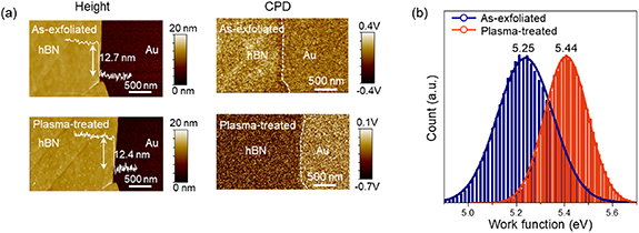
Figure 5. (a) Thickness and contact potential difference (CPD) images before and after oxygen plasma. The dash line denotes the boundary between hBNs and Au substrate. (b) Work function variation of hBNs by oxygen plasma.
Download figure:
Standard image High-resolution imagewhere φtip, φsample, and e are the work functions of the Pt-coated tip and the hBN sample, and the elementary charge, respectively. The CPD of the as-exfoliated hBN shifted from 0.12 V to −0.31 V after the oxygen plasma treatment as shown in figure S5. The work function of the Pt-coated tip was calibrated using a gold film (φAu = 5.05 eV). As a result, the calculated work function of the plasma-treated hBN is 5.44 eV as shown in figure 5(b). This indicates that the Fermi level of the plasma-treated hBN moves closer to its valence band. Figure 6(a) shows the spectra of the valence band maximum (VBM) and conduction band minimum (CBM) of the as-exfoliated and plasma-treated hBNs measured by the PES and NEXAFS, respectively. The PES spectra show that the energy difference between the Fermi level and VBM decreased from 2.5 to 1.7 eV after the plasma-treatment. It indicates that VBM of plasma-treated hBN upshifted toward the Fermi level, which agrees with the work function shift measured in figure 5(b). In the B K-edge NEXAFS spectra (red line) of figure 6(a), π* peak was observed at ∼193.7 eV, which is a characteristic feature of hBN [33]. After the oxygen plasma treatment, the intensity of the π* peak decreased significantly and downshifted by 0.4 eV. Therefore, the band gap of the hBN was reduced from 5.7 to 4.5 eV due to increased defect states as depicted in figure 6(b). This is probably due to the increased bonding length in the disordered crystal structure of hBN after plasma treatment. Our electrical measurements show that the electrical properties of the hBN can be modulated by controlling the density of defects through the oxygen plasma treatment.

Figure 6. (a) PES and NEXAFS spectra of as-exfoliated and plasma-treated hBNs. Blue and red lines indicate the VBM and CBM of as-exfoliated and plasma-treated hBNs, respectively. Black arrow shows the shift of CBM. (b) Schematic of bandgap tuning by oxygen plasma of hBNs.
Download figure:
Standard image High-resolution image
4. Conclusion
In this study, we demonstrated that the electrical properties were significantly modulated by various defects on the surface through the inside of hBN induced by the oxygen plasma treatment. Although the hBN is a representative insulator with a large bandgap, the oxygen plasma process modulates the electrical property of hBN by easily generated the defects and then the bandgap of hBN was reduced from 5.7 eV to 4.5 eV. Raman spectroscopy showed the enhanced PL from specific defects states after a certain duration of oxygen plasma, which indicates the increased density of defects. The DFT calculation elucidated that the types of oxygen-related defects are in good agreement with the PL data. Moreover, the PES analysis revealed that the defect types can be controlled by oxygen plasma via the generation of specific defects such as VB. Our results showed the optical and electrical properties of hBN can be significantly modulated by the oxygen plasma process, and it is an important factor to be considered in the manufacturing process of robust 2D electronic devices using hBN in the future.
Acknowledgments
This work was supported by the National Research Foundation (NRF) of Korea (2018M3D1A1058793, 2017R1A5A1014862 (SRC Program: vdWMRC Center)) and the Creative-Pioneering Researchers Program through Seoul National University (SNU). Kenji Watanabe and Takashi Taniguchi acknowledge support from the Elemental Strategy Initiative conducted by the MEXT, Japan, Grant Number JPMXP0112101001, JSPS KAKENHI Grant Number JP20H00354 and the CREST(JPMJCR15F3), JST. Young Duck Kim acknowledge support from the NRF of Korea (2021R1A2C2093155, 2021M3H4A1A03054856) and grant from Kyung Hee University (KHU-20211033).
Data availability statement
All data that support the findings of this study are included within the article (and any supplementary files).