
Abstract
Screen-printed graphene is integrated with multiple-input multiple-output (MIMO) technology to conquer the most concerned surge in electronic waste caused by the mass deployment of Internet of things (IoT) applications. A flexible MIMO antenna is implemented with simple fabrication process suitable for large-scale production by screen printing graphene highly conductive ink on paper substrate, ensuring high-speed 5G mass data wireless transmission without damaging the ecological environment. This environmental-friendly, low-cost, flexible and conformal MIMO antenna with orthogonal polarization diversity employs co-planar waveguide feed and planar pattern for achieving high space utilization and better integration in most scenarios, for instance, body centric networks and monitoring systems. Excellent performance has been achieved due to the high conductivity of the graphene: the fabricated antenna exhibits an average sheet resistance of  . The bandwidth of the antenna ranges from
  (53.71% fractional bandwidth), covering
  long term evolution, sub-6 GHz
  mobile communication networks, 2.5 and 3.5 GHz WiMAX, and 2.4 and 3.6 GHz WLAN. Within this range, the antenna exhibits effective radiation, also its envelope correlation coefficient remains below
  , manifesting outstanding signal transmission quality in a variety of wireless networks. This work illustrates a novel aggregation of MIMO technology and graphene printing electronics, enabling cheap accessible and green MIMO antennas to be massively integrated in IoT applications.
Export citation and abstract BibTeX RIS

Original content from this work may be used under the terms of the Creative Commons Attribution 4.0 license. Any further distribution of this work must maintain attribution to the author(s) and the title of the work, journal citation and DOI.
1. Introduction
Spurred by the arrival of the 5G revolution, the implementation of Internet of things (IoT) and its extended concept, Internet of everything, have greatly increased the yield requirement of conformal wireless printed electronics as well as the quality of communication networks. Intense efforts have been put in developing nanomaterials with excellent properties and simpler fabrication process with lower cost and higher feasibility. Among all the two-dimensional (2D) materials, graphene has been the most extensively investigated for its prominent properties given by its 2D crystal structure [1], such as its high carrier mobility, conductivity, and high strength.
To produce graphene at high yields, liquid-phase exfoliation of graphite flakes [2] surpasses other approaches such as micromechanical cleavage, dispersion and exfoliation of graphene oxide, growth on metal substrates or annealing on SiC substrates for its high production efficiency and preserve of graphene's electronic structure. This method is also attainable for other 2D materials such as transition metal dichalcogenides, black phosphorus and hexagonal-boron nitride with a variety of solvents [3]. The efficiency of exfoliation is closely related to the ratios of the surface tension component of the solvent and that of the 2D material. These dispersions can then be used to produce ink and deposit flakes on desirable substrates by simple printing methods, realizing mass scalable and fully printable 2D material applications including energy storage, conductive inks, sensors and optical devices [4].
Different printing techniques of 2D materials have been developed on substrates such as polymers, glass and paper [5], exhibiting multi functionalities and promising potentials. However, mass manufacturing of electronic equipments brings mass disposal. Waste disposition of electronics has been an insurmountable obstacle that draws the most concerns. To keep large-scale industrial production compatible with sustainable development, at the same time in pursuit of low cost and flexibility, a large amount of work has been devoted to printing 2D materials on flexible substrate, such as paper, to ensure the biological degradability of electronic devices [6–11]. By taking good advantage of the porosity of paper, printing formulated ink on paper allows fast absorption, enhancing the resolution of pattern and avoiding unwanted diffusion. Graphene, making a good substitution of conventional metal for its high conductivity and strength, environmental amity, and extremely low cost, has been reported fully compatible with paper substrate using simple printing techniques [6–9, 11], which even enhances the robustness of flexible devices including electrodes, transistors, antennas and interconnecting transmission lines, and prevents discontinuities during high-level deformation [12], suitable for large scale manufacture and disposable use.
Sub-6 GHz based 5G architecture has brought IoT applications into the spotlight as they establish interconnection between people and machines and between machines and machines, make information exchange swift, convenient and precise in people's everyday life. The occurrence of multiple-input multiple-output (MIMO) technology is regarded as a significant breakthrough that breaks the data throughput limit existing in conventional single-input single-output systems, provides full use of space resource and multiplies channel capacity, spectral efficiency and data handling capacity without actual extension of frequency usage or any antenna transmitting power increase [13, 14]. The use of MIMO technology is indispensable for the pervasive deployment of IoT smart applications to attain additional functions and requirements, and face massive data throughput for the achievement of low latency, reliability and real-time information exchange [15]. A number of MIMO antennas with large bandwidth designed for 5G cellular networks and IoT platform have been investigated in [16–18], designed with rigid metal and conventional substrates. However, to meet the rapid development of IoT, flexibility of electronic devices is particularly necessary to enhance adaptability and user comfort, yet few efforts have been made using flexible substrate [19, 20]. For instance, MIMO antennas implemented on textiles [19] require large soldering area on the plate, weakening its reconfigurability and sustainability. To attach antenna patterns to substrates, planar conformal antennas, such as printed flexible antennas would be the best choice, thanks to the advances in the modern printed electronic technology. Ink-jet printing silver nanoparticle ink on polyethylene terephthalate substrate can also be a way [20], yet it significantly rises the cost of manufacturing and introduces cracks during heavy deformation.
To fabricate graphene antennas with high pattern accuracy, most work have been focused on using ink-jet printing and screen printing techniques [6–9, 21]. With its extremely low cost and easy process, screen printing transcends ink-jet printing from the perspective of mass production [22]. Screen printed graphene antennas have been reported [6–9, 11, 22–26]. The research is mostly aimed at simple dipole [9, 11, 23] and radio-frequency identification tag antennas [6, 22, 24, 25]. These screen printed graphene antennas exhibit outstanding performances including electrical conductivity, mechanical stability and environmental sustainability, revealing screen printing graphene antennas as a promising candidate for wireless communication and sensing applications, where flexibility, massive production and low cost are especially required, promoting the incorporation of graphene in flexible printed electronics. MIMO technology is essential for 5G wireless communications and high performance IoT applications, guaranteeing high-speed data transmission and system reliability. However, due to the complicated structures induced by MIMO antenna design such as lowering the mutual coupling between antennas, needs of high conductivity and environmentally friendly ink, lack of scalable and affordable fabrication process, screen printed graphene MIMO has yet to be reported.
Here, we present the novel aggregation of two technologies, screen printing MIMO antenna with home-made highly conductive graphene ink [7, 22] on paper substrate, with the aim of integrating low-cost disposable flexible antennas with the 5G IoT applications and increasing the data throughput. A graphene printed, co-planar waveguide (CPW) fed, highly isolated, wideband 4 × 4 MIMO antenna was designed and fabricated by first developing a graphene ink (50 mg ml−1) with a high conductivity of  using N-methyl-2-pyrrolidone (NMP) and viscous ethylene glycol (EG) solvents for screen printing, then depositing the dispersion of graphene flakes on paper substrate with a resolution of 0.4 mm to achieve our designed pattern. The SubMiniature version A (SMA) connectors were then connected to the antennas using conductive epoxy, supporting multiple data transmission links. The MIMO consists of four identical antennas orthogonal to each other and the ground extension stubs altering the current flow. The SEM cross-sectional view, Raman and X-ray photoelectron spectroscopy (XPS) of the printed graphene antenna were investigated. To assess the flexibility of the graphene printed conformal antenna and evaluate its working performance, tests under different bending conditions have been carried out.
This paper is organized as follows. First, the fabrication process and electrical properties of the printed graphene MIMO antenna are elaborated in section 2, involving graphene ink preparation and screen-printing technology. The designs and modeling of the MIMO antenna are then illustrated with effects of parameter alteration, explaining polarization diversity and other mutual coupling reduction techniques. After that, antenna performances with and without bending applied are observed and evaluated. Finally, the work is concluded with some final remarks.
2. Material preparation and electrical properties
The production process of printed graphene can be briefly introduced as (a) shear mixing in chosen dispersant to reduce the physical size of graphite flakes which increase the exfoliation efficiency for the following steps, (b) high power ultrasonication treatment to produce few-layer graphene, (c) initial filtration for the removing of large particles, and tuning the ink to appropriate viscosity, (d) printing and (e) compression. To be specific, the graphene conductive ink was prepared from pristine graphite flakes (Alfa Aesar, 325 mesh, purity: 99.8%). The dried graphite flakes were mixed with NMP (Sigma, anhydrous, purity: 99.5%) at a concentration of 20 mg ml−1 [8], followed by 2 h sheer mixing at 8000 rpm (Silverson L4R mixer) where the temperature was controlled around 20  . (Constant temperature was maintained by circulating water cooling system to prevent overheating.) During this process, the graphite flakes were initially exfoliated. For ultrasonication treatment, NMP solvent was used for graphene exfoliation as it can achieve low residual and excellent stability [2]. It is crucial to properly control sonication parameters, such as sonication time. The sonication time can directly affect the ink conductivity [22]. To maximize the conductivity of printed graphene, 24 h sonication process was applied to the mixture in glass bottle with ultrasonic bath (SHESTO, UT8061-EUK). The temperature was controlled as well. After that, filtration took place by first using 300 mesh stainless steel screen to filter out unexfoliated large graphite particles, then employing Whatman qualitative filter paper (grade 5) on a glass funnel (140 ml Aldrich Buchner) for vacuum suction filtration to remove the remained NMP solvent. The collected solute from the filter paper was then dispersed in EG (Alfa Aesar, anhydrous, purity: 99%) and filtered by the same process to further remove the NMP. The remained solute was again dissolved in EG and centrifuged at low speed (500 rpm) to remove relatively large, unexfoliated graphite flakes. The process was repeated three times. Finally, we collected the graphene nanoflakes dispersion and tuned it to the right concentration for screen printing by vacuum evaporation. The final conductive ink for screen printing was made with a concentration of 50 mg ml−1, ensuring both the smooth deposition of the ink during printing process and the viscosity of the ink.
Screen printing operation was carried out on a semiautomatic screen printer with the assistance of a slant squeegee with the angle of inclination of 70 moving at a chosen constant speed (50–100 mm s−1) for sufficient ink depositing. A 24T mesh printing screen with negatively patterned antenna shape was fabricated by exposing capillary film (ULANO, EZ50-Orange) in an exposure machine with the application of vacuum pressure regulating valve to lock the location of the screen and achieve good resolution. The mesh of the screen was chosen according to the desired pattern accuracy and adequate amount of ink deposition. Higher resolution can be achieved by finer mesh, however, it impedes ink from transferring to substrate.
After printing the designed antenna pattern on paper substrate (Xerox Performer A4 Paper 80 gsm), the antenna prototype is heated at 100 °C for 4 h for volatilizing the dispersant and at the same time preventing the substrate from overheating. A further rolling compression is applied to enhance the printed film conductivity, as printed graphene layer is porous and has high sheet resistance. Rolling compression was operated by a rolling machine (Agile F130 Manual Mill). The compression can reduce the sheet resistance to its tenths, greatly increasing the conductivity [11]. By compression, the surface of printed graphene was visibly smoothened, forming well-aligned laminated structure, allowing better flow of surface current and higher conductivity. Figure 1(a) exhibits the top view of the compressed graphene layer with 10k times magnification.
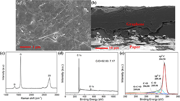
Figure 1. (a) 10k× magnified SEM top view of the screen-printed graphene surface with  scaled bar. (b) 500× magnified SEM cross-sectional view of the antenna with
  scaled bar, the average thickness of the graphene laminate is
  . (c) Raman spectra of printed graphene, (d) wide-scan XPS spectra and (e) deconvolution of C 1s XPS spectra of the printed graphene.
Download figure:
Standard image High-resolution imageSheet resistance characterization with the four-point probe measurement method were performed on ten different positions of the resultant films, 1.9 Ω sq−1 average sheet resistance was achieved.
Good adhesion can be manifested by investigation of the SEM image cross-section in figure 1(b), ambiguous boundary was found between the graphene and paper substrate. The average thickness of the screen-printed graphene layer after rolling compression is measured as  μm. The conductivity can be calculated as
  using equation (1), which is close to a reported work [27], but without the use of high temperature annealing (350
  )
)
where Rs is the sheet resistance. Raman spectroscopy of printed graphene is shown in figure 1(c). The sample is excited from a 532 nm laser source which causes phonon energy shift by Horiba Raman spectrometer. Three main peaks can be spotted at D-band (1347 cm−1), associated with the ring breathing mode of sp2 carbon atoms and typically weak in graphene of high quality, G-band (1575 cm−1), revealing the in-plane vibrational mode of graphite lattice, and relatively wide 2D-band (2704 cm−1), representing an overtone of the D band, resulting from a two-phonon lattice vibration [22, 28, 29]. In figure 1(c), low ID/IG ratio can be observed, indicating very few structural defects on graphene flakes, contributing to highly effective electron flow. To further analyze the surface composition of the graphene, figure 1(d) shows the wide-scan XPS spectra of the printed graphene sample, exhibiting the presence of carbon and oxygen with a ratio of 92.83:7.17. The high ratio of C 1s peak and O 1s peak indicates that only a small quantity of defects exists in the form of oxides, which were possibly inserted during fabrication process [30–32]. Figure 1(e) displays the deconvoluted C 1s XPS spectra of the printed graphene sample with an extremely significant peak at 284.6 eV and a lower peak at 285.2 eV, representing the sp2 and sp3 hybridized carbon respectively. The three much weaker carbon–oxygen peaks are attributed to C–O (286.0 eV), C=O (286.9 eV) and O–C=O (289.1 eV) bonds.
3. Antenna design and simulation
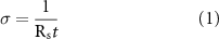
A computer simulation technology (CST) model with labeled parameters of the proposed graphene screen-printed MIMO antenna is displayed in figure 2(a) [33]. Paper substrate has been used in this work for its flexibility, low cost and environmental protection. For impeding the conductive ink from double-sided permeation on paper substrate, we have deployed CPW feeding so as to place the ground on the same side as the antenna.
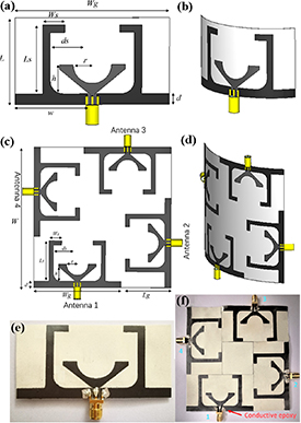
Figure 2. Proposed flexible graphene printed antennas. (a) Designed single antenna model and related parameters. (b) Conformal antenna. (c) Designed MIMO antenna model and related parameters. (d) Conformal MIMO antenna. (e) Screen-printed antenna prototype. (f) Screen-printed MIMO antenna with four identical elements orthogonal to each other.
Download figure:
Standard image High-resolution imageAlso, planar structures ensure compactness of the structure and allowance of better space resource usage. The paper substrate in the simulation has a dielectric constant of 2.3, permeability of 1 and a thickness of 0.1 mm. The loss tangent of 80 gsm paper at room temperature is set to 0.02 according to [34]. The printed graphene layer was modeled as ohmic sheet as its skin depth is much larger than its thickness [7]. The resistance of the modeled graphene sheet was set to 1.9 Ω sq−1 as measured on ten different points each on five printed samples using a four-point probe station (Jandel, RM3000) and semiconductor characterization system (Keithley, 4200C). To improve simulation accuracy, four SMA connectors were modeled at the end of each feeding line, fixing the port impedance at 50 Ω (figure 2(a)).
The design of the conformal graphene printed MIMO antenna was first started with the individual antenna structure, as presented in figures 2(a) and (b). The round outline of the graphene helps broadening the bandwidth of the antenna. The performances of three configurations for single antenna design evolution are exhibited in figure 3 to estimate the effects of the stub extensions of different shapes. Antenna I features two inverted L-shaped stubs extended from the ground, whereas Antenna II only consists of bare ground and Antenna III contains I-shaped extensions (all the rest parameters are the same).
Figure 3. Simulated results for three configurations of stub extensions. (a) Three configurations. (b) Surface current of three configurations at 2.4 GHz. (c) Return loss of three antennas. (d) Total efficiencies of the antennas. (e) Realized gain plots of the antennas.
Download figure:
Standard image High-resolution imageAs shown in figures 3(b) and (c), which compare the surface current and return loss of the three patterns, Antenna II does not resonate at 2.4 GHz as Antenna I and III do and stronger surface current in Antenna II at 2.4 GHz is gathered at the feeding line instead of radiating parts. To compensate this, Wg needs to be increased by more than 20 mm, severely degrading the compactness of the antenna. Furthermore, from the plots depicted in figures 3(d) and (e), with the occurrence of the I-shaped stubs, a significant rise in gain and efficiency at 2.2–3 GHz can be observed. This is because the extension stubs not only improve the matching of the antenna at lower frequency without enlarging structural size, but also enhance the radiation orthogonal to the antenna plane [35]. The bar of the inverted L-shape further improves the gain at lower frequency as seen from the surface current of Antenna I. The extension stubs radiate sufficient power as the main radiating element at 2.4 GHz with enhanced efficiency. Therefore, Antenna I is selected as a desirable compact antenna with reasonable bandwidth, efficiency and gain.
Parametric study of the antenna is crucial to achieve desirable characteristics. Effects of graphene sheet resistance on antenna performance are shown in figures 4(a) and (b), revealing that while the return loss is not very sensitive to the change of the sheet resistance, 1 Ω sq−1 reduction in sheet resistance can bring the realized gain down by about 1 dB. Parameters listed in table 1, such as feeding line length d and ground width Wg of the antenna have been studied and optimized, presented in figures 4(c) and (d), so that full excitation of the antenna for signal transmission at its operating frequency bands is guaranteed and unnecessary power dissipation in the feeding line can be avoided.

Figure 4. Simulated results for parametric analysis. The influence of sheet resistance Rs (Ω sq−1) on (a) S11 and (b) gain of the proposed antenna. The impact of (c) feeding length d, (d) width Wg and (e) distance of the stub ds on magnitude of S11, (f) stub length Ls on gain.
Download figure:
Standard image High-resolution imageTable 1. Dimensions of the proposed graphene-printed antennas.
| Parameters | mm | Parameters | mm |
|---|---|---|---|
| Single antenna | |||
| Substrate length, L | 40 | Circle radius, r | 8.67 |
| Stub length, Ls | 31.68 | Substrate width, Wg | 70 |
| Feeding length, d | 5 | Height of patch, h | 13.3 |
| Distance of stub, ds (from the edge of the ground) | 17.2 | Width of stub, Ws | 10 |
| Ground width, w | 33.1 | ||
| MIMO antenna | |||
| Length of MIMO, W | 110 | Distance of stub, ds | 17.2 |
| Width of element, Wg | 70 | Circle radius, r | 8.67 |
| Length of element, Lg | 36.68 | Height of patch, h | 13.3 |
| Stub length, Ls | 31.68 | Width of stub, Ws | 10 |
| Feeding length, d | 5 | ||
By comparing the S11 plots in figures 4(d) and (e), it is proved that the distance of the stubs on the sides alters the resonant frequency of the antenna instead of the ground width Wg, and by adjusting the length Ls of the stubs, the realized gain can be optimized within the operating frequency band as shown in figure 4(f).
Moreover, the function of the inverted L-shape stub in MIMO antenna performance (Antenna I) is not only limited to gain enhancement and size reduction, it also reduces the mutual coupling between the antenna elements as it suppresses the surface current on the antenna plane. The simulation results for return loss (S11) and isolation (S12 and S13) of MIMO antenna I and II are displayed in figures 5(a) and (b). As seen from the comparison, for frequency higher than 2.7 GHz, more than 10 dB decrease in S13 and 3 dB in S12 are achieved with the insertion of ground extension stubs, indicating higher isolation in both directions and higher gain at desired frequency. When Rs= 4 Ω sq−1, in figure 5(b), a 2 dB drop in gain occurs comparing with the gain curve of Rs = 1.9 Ω sq−1, conforming to the observation from figure 4(b) that gain decreases with the increase of Rs.
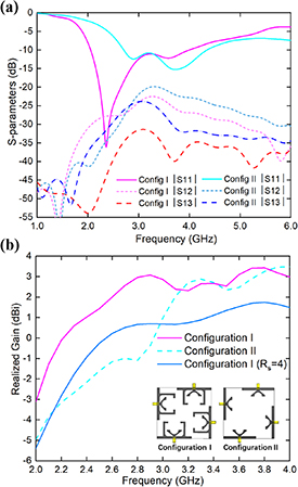
Figure 5. Comparison of simulated results for (a) S-parameters and (b) realized gain of two different configurations (with and without ground extension stubs).
Download figure:
Standard image High-resolution imageAnother desirable feature which should also be highlighted is the orthogonal placement of the four single antennas. Four single identical antennas are positioned perpendicularly to each other, with the intention of mitigating correlation with orthogonal polarization diversity, which can void spatial correlation and decrease structure size. Thus, interference between adjacent antennas, when two or more ports are activated, is lowered to a great extent, achieving good isolation with less spatial resource.
4. Measurement results and discussions
Figure 2(f) shows the fabricated conformal screen-printed graphene MIMO antenna on paper substrate. Four 50 Ω SMA connectors were connected to four CPW feeding point by using conductive epoxy. A vector network analyzer (VNA Agilent E5071B) was used to determine the scattering parameters of the printed graphene MIMO antenna. A horn antenna was employed in an anechoic chamber for two-antenna method with its known performance, measuring the radiation pattern and gain of the fabricated antenna. The setup of experiment apparatus is illustrated in figure 6, where the distance between the horn antenna and the printed graphene antenna was fixed to 0.8 m.
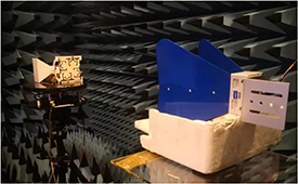
Figure 6. Antenna measurement set up with a horn antenna in anechoic chamber, the distance between the horn antenna and the MIMO antenna under test is 0.8 m.
Download figure:
Standard image High-resolution imageFor the ease of measurement, the antenna was supported by a flexible screen made of polypropylene with relative permittivity of 2.27, loss tangent of 0.002 at 1 GHz and permeability of 1 [36]. By comparison, the use of flexible screen leads to a tiny shift (about 50 MHz) to lower frequency, which should have minimal effect on antenna performance according to the simulation results in figure 7(a) and gain in figure 7(b). Due to the unique design of the structure, identical performance can be observed for antennas 1 and 3, likewise for antennas 2 and 4. Thus, for a clearer display of the scattering parameters of the MIMO antenna, only S11, S12 and S13 are shown in figure 7(a).

Figure 7. (a) Measured and simulated scattering parameters with and without flexible screen, (b) simulated realized gain with and without screen with different resistances, and measured gain using a standard horn antenna.
Download figure:
Standard image High-resolution imageA good agreement between the simulated and measured S-parameters can be observed. The 10 dB bandwidth of the antenna is 2.22–3.85 GHz from the measurement and 2.05–3.89 GHz from the simulation. The discrepancy may be caused by the material parameter variations due to screen printing and after-printing processes, such as compression tolerance, e.g. the uneven surface caused by manual control of compression (hence causing conductivity variation), the difference in the dielectric constant of paper substrate from the simulation or less perfect contact between the conductive epoxy and the feeding. It is important to note that, the licensed global 5G spectrum in mid band range is entirely covered by this wide bandwidth of the antenna in the test.
From measured S12 and S13 in figure 7(a) we can see that the isolation between two orthogonally placed antennas is below −30 dB, realizing excellent mutual coupling reduction within the desired frequency band. This is achieved by altering the orientation of the adjacent antennas and stubs. Even lower mutual coupling can be found between opposite antennas, as it can be seen that the value of S13 is about 10 dB lower than S12 in both simulated and measured results. Figure 7(b) compares the simulated realized gain to the measured gain of the MIMO antenna with the support of flexible screen, obtained with a horn antenna by two-antenna method. Apart from an average 2 dB fall in magnitude, which most likely to be caused by higher sheet resistance than expected sheet resistance (1.9 Ω sq−1 was used in the simulation) as verified in figure 4(b) (the impact of sheet resistance on gain reduction), the shape of the measured gain is in good agreement to the simulated within the operating frequency band. The measured gain features 0.4 dBi at 2.4 GHz and 0.56 dBi at 3.5 GHz, reaches its peak value 0.92 dBi at 2.6 GHz, acceptable for low-cost disposable use for 4G long term evolution (LTE), WiMAX and 5G mid-band applications. Simulated and measured radiation patterns in both E- and H-plane at 2.4 GHz and 3.5 GHz are plotted in figure 8 respectively.

Figure 8. Normalized simulated and measured radiation patterns on E-plane and H-plane at 2.4 GHz and 3.5 GHz.
Download figure:
Standard image High-resolution imageThe directivity is maximized on the orthogonal plane of the antenna plane, i.e. 0° and 180°. As can be observed, the measured patterns are in acceptable agreement with simulated ones.
For a more precise illustration of the achieved isolation, the envelope correlation coefficients (ECCs) of both opposite and adjacent antennas are calculated using equation (2) [37]
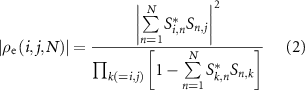
where N is the number of antennas, i = 1 to n, j = 1 to n.
From 2 to 6 GHz, the ECC values between both of the adjacent antennas and opposite antennas, as seen in figure 10(c), indicating negligible correlation (ECC <  for the whole desired frequency range), fully testifies the transmission quality of each antenna in the structure.
To accomplish the 5G network revolution blueprint and bring high-quality IoT to everyday life, it is crucial not only to deal with massive data throughput, conformability of electronic elements is also an essential factor to attain better adaptability, usability and sustainability in applications, such as user-interactive health monitoring systems, virtual reality gaming systems, vehicle to vehicle communications, robotics and autonomous systems. By being attached to human bodies who take part in physical activity monitoring systems, conformal antennas provide better user comfort than the ones which consist of rigid metals. To bend the antenna to a desired angle, a scaled adjustable and flexible screen was designed and fabricated, shown in figure 9(a). The bending of the screen can be adjusted by altering the arc. During the conformability tests, the MIMO antenna was supported by this flexible screen in an anechoic chamber.
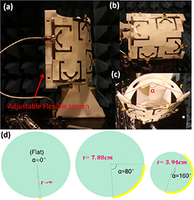
Figure 9. (a) Front view of the screen-printed graphene MIMO antenna being vertically bent by α = 160° on a scaled adjustable flexible screen with one of its ports connected to the vector network analyzer, and (b) horizontally bent by 120°, (c) top view of the antenna when fixed on the flexible screen with r = 5.3 cm and α = 120°. (d) Bending with α = 0°, 80° and 160°. The yellow arc represents the curved side length of the antenna (W = 110 mm).
Download figure:
Standard image High-resolution image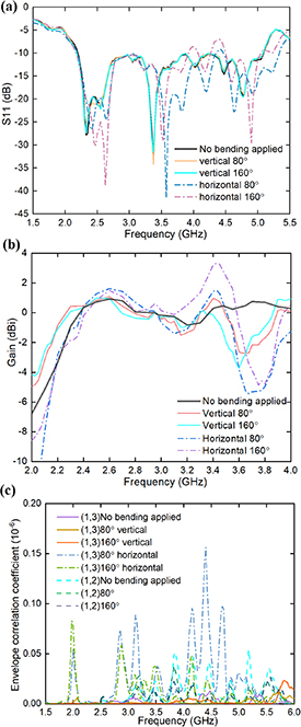
Figure 10. (a) Measured reflection coefficient variation with increasing bending with α = 0° (when no bending is applied), 80° and 160° vertically and horizontally respectively, (b) measured antenna gain with vertical and horizontal bending alteration, (c) envelope correlation coefficient (ECC) between antenna 1 and 2, and antenna 1 and 3 calculated from measured scattering parameters.
Download figure:
Standard image High-resolution imageBoth vertical and horizontal bending, shown in figures 9(a) and (b), were conducted separately to inspect the performance of the antenna with increasing bending stress. As tested, the bending limit for the antenna to remain at its working condition is at α = 160°, where α refers to the angle between the two radii that form the arc, as shown in figure 9(c). Imagining the flexible screen as a cylinder, the antenna is attached to this cylinder with an adjustable radius r. By adjusting the supporting arc behind the flexible screen, bending conditions with α = 80° and 160° are realized for conducting S-parameters and ECC tests. The corresponding radii for α = 80° and 160° are r = 7.88 and 3.94 cm respectively, as shown in figure 9(d), where the length of the arc in yellow is fixed at W = 110 mm, and α = 0° indicates infinite radius and flat surface. Figure 9(a) shows when the antenna is being vertically inflected with α = 160°.
S11 variations with vertical and horizontal bending can be observed in figure 10(a). It can be seen that the resonant frequency does not move much during the bending tests but the reflection coefficient is distorted more when horizontal bending is applied. This is due to the ground extension stubs experience deformation to a greater extent in horizontal case. Figure 10(b) reveals that the gain changes more for horizontal bending than that for vertical bending; the peak gain goes up to 3.3 dBi for horizontal 160° bending and 1.3 dBi for 80° bending at about 3.5 GHz. The gain remains at 0.4 dBi with all bending cases around 2.4 GHz. There are dips occurring around 3.7 GHz for both bending cases, which could be caused by the deformation in radiating elements.
The ECC values for the bending cases can be simply derived from our measured scattering parameters using equation (2). Due to the special rotational symmetry of the MIMO antenna, we consider ECC in terms of the relative positions of the elements for simplicity, that is, ECC(1, 2) should behave like ECC(3, 4) with same bending action applied, correspondingly, ECC(1, 3) should behave the same as ECC(2, 4). Hence, the adjoining antennas (1, 2) and opposite antennas (1, 3) with different curvatures are inspected in figure 10(c). Note that the orientation of bending makes no difference in ECC between adjoining antennas. From observation, ECC values for all conditions are below  for the entire operation frequency. At 2.4 GHz, the isolation even improves between adjacent antennas for horizontally bent opposite antennas since the bending alters the polarization and the relative position of the two antennas, reducing the interference along horizontal axis.
Also, the channel capacity loss (CCL) between two antenna elements in figure 11 is estimated by equations (3)–(5) [38]


Figure 11. Channel capacity loss between antennas with and without being bent calculated from measured scattering parameters.
Download figure:
Standard image High-resolution imageDespite the compact arrangement of the antennas, the value of CCL remains below 0.2 bits s−1 Hz−1 from 2 to 6 GHz even with 160° bending applied, where the standard CCL for a  MIMO antenna is 0.4 bits s−1 Hz−1 [38]. The loss between adjacent antennas can be spotted a little higher than opposite polarized antennas due to the closer separation and polarization correlations.
Antenna radiation characteristics at 2.4 GHz and 3.5 GHz respectively with α = 0°, 80° and 160° can be examined from figures 12 and 13. In figure 12(a), more offset of maximum directivity of the antenna in E-plane at 2.4 GHz can be seen with increasing vertical curvature than that of the case of horizontal curvature. This is because, when the MIMO antenna is being bent vertically, two side stubs are not co-planar anymore. At 2.4 GHz, the power is mainly radiated by the side stubs, as shown in figure 3(b) (the surface current of Antenna I at 2.4 GHz), thus, changing the direction of the stubs causes the radiation distortion in E-field at 2.4 GHz. However, at 3.5 GHz, power is mostly radiated by the patch rather than the stubs, so that vertical bending does not break the radiation symmetry of element, as shown in figure 12(b). Other than this, the antenna consistently remains at its normal working condition with horizontal bending. Radiation patterns in magnetic field at both 2.4 GHz and 3.5 GHz can be observed in figure 13. Similarly, the field alters a little more when vertical bending applies than horizontal bending, however, this slight alteration in fields barely alters the transmission. In general, the antenna preserves its good radiation performance up to the bending angle of 160°, despite slight diversity change in electric field due to the break of symmetry, revealing good adhesion and stable power transfer performance of the antenna. Cross polarizations of the antenna under different bending conditions in E- and H-plane are measured and shown in figures 12 and 13. The results are normalized with respect to the maximum value of the co-polarization results. It can be observed that the cross-polarization results at broadside are about 30 dB and 20 dB down compared with the co-polarization levels in E and H-plane respectively at both 2.4 and 3.5 GHz under all bending conditions up to 160 , revealing good radiation performance. It can also be observed that vertical bending affects more on cross-polarization orientation at 2.4 GHz due to the same reason as discussed on co-polarization variation by vertical bending at 2.4 GHz.
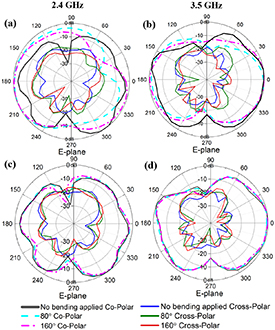
Figure 12. Normalized MIMO antenna radiation pattern on H-plane at (a) 2.4 GHz with vertical bending, (b) 3.5 GHz with vertical bending, (c) 2.4 GHz with horizontal bending and (d) 3.5 GHz with horizontal bending with α = 0°, 80° and 160°.
Download figure:
Standard image High-resolution image
Figure 13. Normalized MIMO antenna radiation pattern on H-plane at (a) 2.4 GHz with vertical bending, (b) 3.5 GHz with vertical bending, (c) 2.4 GHz with horizontal bending and (d) 3.5 GHz with horizontal bending with α = 0°, 80° and 160°.
Download figure:
Standard image High-resolution image
5. Conclusion
In this paper, a novel aggregation of graphene printing electronics and MIMO technology has been presented, enabling cheap accessible MIMO antennas to be massively deployed in various IoT applications. A conformal, well-isolated, environmental-friendly, screen-printed graphene MIMO antenna has been designed, fabricated and characterized, confirming the feasibility of using highly conductive printed graphene to promote the flexibility and biodegradability of high reliability and fast data transmission devices. Good isolation is evident with its extremely low ECC value below  for the entire desired frequency band with acceptable gain as a result of the ground extension stub and polarization diversity design. The conformability and usability of the antenna have been testified that it remains working for bending angle below 160°, suitable for most user case scenarios with good adhesion and stable power transmission. The bandwidth of the antenna covers a wide range of applications, including 4G LTE telecommunications networks, 2.45 GHz industrial, scientific, medical, sub-6 GHz 5G mobile networks, WLAN and WiMAX applications. The low manufacturing cost and disposable features of this graphene printed MIMO antenna reveal its potential for massive production for 5G dense communication networks deployment. Furthermore, its compact size and flexibility directly lead to greater integration in flexible 5G front-ends, IoT systems, as well as in next-generation wearable electronic devices.
Acknowledgments
This work was supported in part by the UK Engineering and Physical Research Council under Grant No. EPN010345 and EU Graphene Flagship Program.
Data availability statement
All data that support the findings of this study are included within the article (and any supplementary files).