
Abstract
The functional form of Coulomb interactions in the transition metal dichalcogenides (TDMs) and other van der Waals solids is critical to many of their unique properties, e.g. strongly-correlated electron states, superconductivity and emergent ferromagnetism. This paper presents measurements of key excitonic energy levels in MoSe2/WSe2 heterostructures. These measurements are obtained from resonance Raman experiments on specific Raman peaks only observed at excited states of the excitons. This data is used to validate a model of the Coulomb potential in these structures which predicts the exciton energies to within ∼5 meV. This model is used to determine the effect of heterostructure formation on the single-particle band gaps of the layers and will have a wide applicability in designing the next generation of more complex TDM structures.
Export citation and abstract BibTeX RIS
One of the key reasons for the unique properties of van der Waal's structures is that the reduction of dielectric screening in these 2D systems leads to enhanced Coulomb interactions with functional form quite different from the standard 3D Coulomb potential [1, 2]. This Coulomb potential leads to the renormalisation of the single particle electronic energy and an increase in the band gap [3, 4]; exciton states which follow a non-hydrogenic series [5] with large oscillator strengths and short radiative lifetimes [6–8]; and stable multi-particle states such as trions [9–12]. It is critical to the existence of strongly-correlated states leading to optically accessible incompressible electron states, superconductivity [13, 14], and emergent ferromagnetism [15]. It is responsible for the existence of interlayer excitons in transition metal dichalcogenide (TMD) heterostructures and their mutual repulsion leading to a density dependent blue shift of their emission [16]. The exchange component of the Coulomb interaction is responsible for mixing of the A and B excitons with implications for spintronics [17].
The importance of quantifying the Coulomb interaction in TMD monolayers has led to a series of experiments aimed at measuring the energy of the bright, zero orbital angular momentum (s), excitonic states in these structures using a variety of techniques including reflectivity [5, 18, 19], photoluminescence excitation [6, 20], and magneto-photoluminescence [21–23]. In addition two-photon absorption measurements have been performed to allow the energy of the one angular momentum (p) states to be determined [24]. However, despite the wider range of exciting physics, e.g. interlayer excitons, which can be accessed in TMD heterostructures, there are no reliable measurements of the energies of intralayer (single layer) excitons beyond the minimum energy 1s state in such structures. In this paper we discuss the determination of the energy of the (intralayer) A2s and B2s states in a MoSe2/WSe2 bilayer heterostructure with accuracies of a few meV in most cases. The method relies on unique Raman peaks only observed at 2s transitions which enable the unequivocal assignment of specific spectral features to these transitions. Additionally, we demonstrate that it is possible to theoretically reproduce these energies to within the errors of the experiments, i.e. 2.5%, using a model whose parameters can be calibrated with monolayer exciton energies and constrained by separate experiments, and properly takes into account the distance dependent screening.
The results presented here are part of a larger study of high quality hBN encapsulated MoSe2 and WSe2 monolayers [8] and MoSe2/WSe2 heterobilayers [25, 26], with twist angles 2°, 6°, 20°, 57° and 60°, using resonance Raman and reflectivity spectroscopy. All measurements were performed with the samples held at 4 K in the low excitation intensity regime (<100 µW). The resonance Raman studies were performed with excitation photon energies from 1.6 to 2.27 eV allowing us to probe the MoSe2 A1s, A2s, B1s and B2s and WSe2 A1s, A2s and B1s excitonic resonances. The Raman scattering intensity has been calibrated using absolute scattering rates for the silicon peak at 520 cm−1 and corrected for Fabry–Perot effects [27, 28].
Colour plots of the Raman results for MoSe2 and WSe2 monolayer and two MoSe2/WSe2 twisted heterostructures, with twist angles of 57° and 20°, for excitation energies spanning the MoSe2 A1s and B1s intralayer excitons and the WSe2 A1s intralayer excitons are presented in figures 1–3 respectively along with representative Raman spectra at key excitation energies.
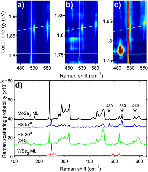
Figure 1. (a)–(c) Resonance Raman colour maps of a MoSe2 (ML) (a) and two MoSe2/WSe2 heterostructures with twist angles of 57° (b) and 20° (c). The three key Raman peaks, that are only observed at the 2s resonances of MoSe2 have their frequencies marked at 480, 530 and 580 cm−1. The colour maps are presented with a logarithmic scale for the intensity to enhance the weaker peaks. The light blue lines represent the energies of the incoming (solid) and outgoing (dashed) resonances with the MoSe2 intralayer A2s exciton (see S3 in the supplementary information (available online at stacks.iop.org/2DM/8/035047/mmedia) for additional discussion of incoming/outgoing resonances). The energy of the exciton was determined by fitting the resonance behaviour of key Raman peaks and is presented in table 1. (d) Raman spectra for the MoSe2 (ML) and two MoSe2/WSe2 heterostructures plus a WSe2 monolayer at the outgoing resonance energy of the A2s exciton, showing the key Raman peaks with their frequencies marked by arrows.
Download figure:
Standard image High-resolution image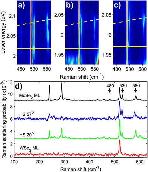
Figure 2. (a)–(c) Resonance Raman colour maps of a MoSe2 monolayer (ML) (a) and two MoSe2/WSe2 heterostructures with twist angles of 57° (b) and 20° (c) across the MoSe2 B2s intralayer exciton resonance. The three key Raman peaks, that are only observed at the 2s resonances of MoSe2 have their frequencies marked at 480, 530 and 580 cm−1. The plots are presented with a logarithmic scale for intensity to enhance the weaker peaks. The yellow lines represent the energies of the incoming (solid) and outgoing (dashed) resonances with the MoSe2 intralayer B2s exciton. The energy of the exciton was determined by fitting the resonance behaviour of the key Raman peaks and is presented in table 1. (d) Raman spectra for the MoSe2 monolayer (ML) and two MoSe2/WSe2 heterostructures plus a WSe2 monolayer at the outgoing resonance of the MoSe2 B2s exciton, showing the key Raman peaks with their frequencies marked by arrows.
Download figure:
Standard image High-resolution image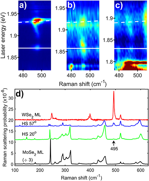
Figure 3. (a)–(c) Resonance Raman colour maps of a WSe2 monolayer (ML) (a) and two MoSe2/WSe2 heterostructures with twist angles of 57° (b) and 20° (c) for excitation energies near the WSe2 A2s intralayer exciton resonance. The key A2s specific Raman peak is at around 495 cm−1. The plots are presented with a logarithmic scale for intensity to enhance the weaker peaks. The white lines represent the energies of the incoming (solid) and outgoing (dashed) resonances with the WSe2 intralayer A2s exciton. The energy of the exciton was determined by fitting the resonance behaviour of the key Raman peak and is presented in table 1. (d) Raman spectra for the WSe2 monolayer (ML) and two MoSe2/WSe2 heterostructures plus a MoSe2 monolayer at the outgoing resonance of the WSe2 A2s exciton. The frequency of the associated 495 cm−1 Raman peak is marked with an arrow.
Download figure:
Standard image High-resolution image
Table 1. Energies of the various excitonic transitions obtained by fitting from the Raman results for hBN encapsulated vdW MoSe2/WSe2 heterostructure samples (HS) with twist angles of 57 and 20² and their constituent monolayers (ML).
| Measured exciton energy in sample (eV) | |||||
|---|---|---|---|---|---|
| Material | Exciton | MoSe2 ML | WSe2 ML | HS (57°) | HS (20°) |
| MoSe2 | A1s | 1.648 ± 0.001 | — | 1.620 ± 0.001 | 1.623 ± 0.001 |
| MoSe2 | A2s | 1.803 ± 0.002 | — | 1.754 ± 0.001 | 1.765 ± 0.002 |
| MoSe2 | B1s | 1.858 ± 0.001 | — | 1.839 ± 0.001 | 1.849 ± 0.001 |
| MoSe2 | B2s | 2.016 ± 0.001 | — | 1.961 ± 0.016 | 1.969 ± 0.004 |
| WSe2 | A1s | — | 1.740 ± 0.001 | 1.728 ± 0.002 | 1.718 ± 0.002 |
| WSe2 | A2s | — | 1.871 ± 0.001 | 1.857 ± 0.003 | 1.835 ± 0.004 |
| WSe2 | B1s | — | 2.166 ± 0.001 | 2.161 ± 0.007 | 2.164 ± 0.001 |
As previously observed, the Raman spectra of the samples present a large number of distinct Raman peaks [8, 29, 30]; 18 in MoSe2 and 16 in WSe2. The Raman peaks show clear resonance behaviour with significant enhancements associated with either the incoming or outgoing photons being at the same energy as one of the bright excitonic states in the two materials. The energy of the two conditions for each of the 2s excitons are presented on the figures using a solid line for the incoming resonance and a dashed line for the outgoing resonance. Despite the Raman scattering at the A1s and B1s excitonic resonances being approximately two orders of magnitude stronger than at the A2s and B2s, key phonons which are only observed at these 2s resonances [8] allow them to be clearly identified. In the case of MoSe2 the 2s specific peaks are at 480, 530 and 580 cm−1 (see figures 1 and 2 and [8]). We assigned these peaks to two phonon Raman scattering via the 2A1' (Γ), E'(Γ) + A1'(Γ) and 2E'(Γ) phonons respectively [8]. As shown in the colour plots in figures 1 and 2, the peaks have a clear outgoing resonance with the A2s state and incoming and outgoing resonances with the B2s states. In the case of WSe2 there is a unique Raman feature which is only observed at the A2s [8]. This feature is a peak with a characteristic dispersion/resonance behaviour. It starts as a single peak at 495 cm−1 at the incoming resonance energy with intensity that drops to zero for energies just above. It reappears when the laser is tuned to approximately half way between the incoming and outgoing resonances. The peak then disperses to lower shift by 2.5 cm−1 with increasing laser energy until excitation energies close to the outgoing resonance at which point its magnitude increases significantly and it splits into three closely spaced peaks; see SI for more details. There are no differences in the behaviour of the 2s specific peaks between heterostructures and monolayers that cannot be explained by a change in the energy or width of the excitonic transitions.
Now that we have identified the key Raman peaks, we can extract their resonance profiles and fit them to obtain the energy and width of the transitions associated with the excitons. The resonance profiles of the peaks associated with the MoSe2 A2s resonance (480, 530 and 580 cm−1) in the heterostructures were fitted to a Lorentzian lineshape at the outgoing resonance energy. The energy of the phonon was then subtracted to give the energy of the excitonic state. In the case of the MoSe2 B1s resonance the standard third order perturbation prediction (shown in supplementary section S3) for the Raman scattering was used to fit both incoming and outgoing resonances. For the WSe2 A2s, the outgoing resonance was fitted using a Lorentzian lineshape; the complexity of this resonance (shown in supplementary section S5) makes fitting both incoming and outgoing resonances with a third order perturbation model impossible and the outgoing resonance fit is simpler. The energies for the various exciton states obtained from these fits and fits to the resonance profiles of the A1' phonon at the A1s and B1s excitons are summarised in tables 1 and 2; the linewidths and a brief discussion of them is given in the SI. In table 3 we present results for the difference in energy between different excitonic states in monolayers of MoSe2 and WSe2 from the literature. Where comparison is possible, the results from the current resonance Raman experiments and the literature monolayer results are in agreement to within experimental error.
Table 2. Energy separations between key excitonic transitions within each sample determined from the results in table 1 plus predictions for these energies from the model described in the main body of the paper. The agreement between experiment and theory is to within twice the error estimates in all cases.
| Energy differences for exciton states (meV) | ||||||||
|---|---|---|---|---|---|---|---|---|
| Material | Exciton | MoSe2 ML | WSe2 ML | Heterostructures | ||||
| Experiment | Theory | Experiment | Theory | (57°) | (20°) | Theory | ||
| MoSe2 | A1s-A2s | 155 ± 3 | 152.3 | — | — | 134 ± 2 | 142 ± 3 | 138.2 |
| MoSe2 | B1s-B2s | 158 ± 2 | — | — | — | 122 ± 17 | 120 ± 3 | — |
| MoSe2 | A1s-B1s | 210 ± 2 | — | — | — | 219 ± 2 | 226 ± 2 | — |
| WSe2 | A1s-A2s | — | — | 131 ± 1 | 130.2 | 129 ± 4 | 117 ± 4 | 122.4 |
| WSe2 | A1s-B1s | — | — | 426 ± 2 | — | 433 ± 8 | 446 ± 3 | — |
Table 3. Comparison of the difference in energy between different excitonic states in MoSe2 and WSe2 monolayers predicted using the theory discussed in the main body of the paper with previously published experimental values. There is excellent agreement which is within the experimental errors where these are available.
| Energy differences for exciton States (meV) | |||
|---|---|---|---|
| Material | Exciton | Literature experimental values | Theory |
| MoSe2 ML | A1s-A2s | 151[19]; 150[31] | 152.3 |
| WSe2 ML | A1s-A2s | 131[23]; 131[21]; 130[18] | 130.2 |
| WSe2 ML | A1s-A3s | 157[23]; 152[21]; 152[18] | 151.0 |
| WSe2 ML | A1s-A4s | 161[23]; 161[21] | 157.9 |
As presented in tables 1 and 2, the energies of the intralayer exciton states and the 1s–2s separations are both significantly reduced in the heterostructures. As the binding energy of the excitons scale with the 1s–2s separation [3] we can conclude that the binding energy of the excitons is reduced in the heterostructures. This fact combined with the reduction in the absolute energy of the A1s excitons means we can also conclude that the single particle band gaps of the heterostructures must be reduced and by more than the binding energy of the excitons. In addition to the differences between monolayers and heterostructures there are clearly smaller differences in the energies of the various states in the two heterostructures. Whilst it would be tempting to analyse these in terms of twist dependent hybridisation effects, we feel that the possibility of sample to sample variations, independent of twist angle, means it would be premature to do this at this point.
In order to go further in our interpretation of the results we require a theory for the excitonic energies in the heterostructure. Our model is based upon that set out in [32]. We model the MoSe2 and WSe2 layers as infinitesimally thin films possessing only in-plane electric polarizabilities  and
and  , respectively, separated by an interlayer distance
  and embedded in a bulk dielectric medium representing the hBN encapsulation. In the case of a single layer this model leads to the standard Keldysh potential. We then solve the electrostatic problem to obtain an effective interaction between charge carriers within a given TMD layer. This simultaneously includes screening from the layer itself, from the opposite TMD layer, and from the encapsulation (see SI). Once the interaction is known, the intralayer exciton spectra are obtained by solving the corresponding Wannier equations. This requires a number of parameters that are separately constrained by experiments: the electron and hole masses, which we have taken from angle-resolved photoemission spectroscopy (ARPES) [33] and magneto-transport experiments [34, 35]; the in- and out-of-plane dielectric constants of hBN,
  and
and  [36, 37]; and the interlayer separation
  , taken as the average interlayer distance in bulk MoSe2 and WSe2 [38, 39]. The latter value lies at the bottom end of the range of layer step distances measured for MoSe2 monolayers on WSe2 by atomic force microscopy (AFM) [40, 41]. As a result, the model contains only two free parameters,
  and
and  , which we have constrained by six pieces of experimental data: the A2s-A1s energies for the two monolayers and the heterostructures reported here, as well as the A4s-A1s and A3s-A1s energies for monolayers reported by Liu et al [21] and Chen et al [23]. (table 3). Using
  and
and  , our theory reproduces all six exciton energy splittings to within 2.0%, all values being within twice the experimental error for these energies (table 2). As shown in table 2 these also fall within twice the estimated errors of the experimental values. Thus, whilst it is not obvious that the simplification of treating the layers as thin relative to their separation will work there is currently no need for a more complicated model.
It is worthwhile mentioning that further simplifications to the interaction model described above have a significant impact on its accuracy. For instance, treating the encapsulating medium as an isotropic dielectric with average dielectric constant of  increases the minimum error to 5%, or four times the experimental error for the six exciton energies. As discussed in the SI, in the limit of large separation between the charges the interaction takes the form of the Keldysh potential with the effective electric polarizability
  . This coincides with the long-range limit of interlayer interactions studied in [32], where it was found that this approximation underestimates screening at short distances. Here, we find that this approximation for the intralayer interaction has the opposite shortcoming, severely underestimating the strength of short range interactions by overestimating the screening contribution from the opposite layer, leading to errors of up to 30% when comparing to the measured spectra.
Based upon the agreement between theory and experiment we can now predict the excitonic binding contribution to the shift in the energies of the A1s excitons when forming the bilayers. The theory gives the difference in the binding energies of the A1s excitons in monolayers and the heterostructure are −8 ± 0.5 meV for WSe2 and −19 ± 1 meV for MoSe2. The small predicted errors are due to the fact that changes in the model's input parameters cause correlated changes in the monolayer and heterostructure energy predictions. In addition to changes in the excitonic binding energies there are two other contributions to the changes in the exciton energies on formation of the heterostructure; hybridisation of the excitons and changes in the single particle band gaps. Raman scattering has been shown to be sensitive to hybridisation of excitons [25] and there is no evidence for strong hybridisation of any of the excitons discussed in this paper. Therefore, we can conclude that the only other significant contribution to the absolute energies of the excitons is changes in the single particle state energies and therefore we find that the decrease in the single particle band gaps on formation of the heterostructure are 35 ± 2 meV for MoSe2 and 46 ± 5 meV for WSe2.
Whilst so far, we have focussed on the A excitons we also have results for the MoSe2 B 1s and 2s excitons. In the MoSe2 monolayer, we find a slightly larger 1s-2s separation for the B exciton (table 2). This is consistent with ab initio predictions [42] of larger effective masses for both the B electron and hole. In the heterobilayer the MoSe2 1s-2s separation for the B exciton is 10–20 meV less than for the A excitons. It is not possible to explain this using the current theory without a reduction of the electron or hole masses associated with the B exciton of around 50%. There is no experimental or theoretical reason for believing such a reduction occurs in a heterostructure. Instead, it is likely that some other effect beyond the current theory is occurring. Due to the higher energy of the B excitons there may be more states available for hybridisation which could affect the energy of the 1s and 2s excitons differently. However, hybridisation is likely to be twist angle dependent and the B 1s-2s energy differences measured in the two samples are remarkably similar considering one is near 0° twist and one near 60° twist. Despite our inability to fully explain the B excitons in terms of geometry modifications of the Coulomb interaction it is remarkable that it is possible to explain the energy of the A excitons in the heterostructure and the monolayers using the same set of parameters for the dielectric and band structure properties and the separately constrained interlayer separation distance.
The results presented here are an important advance in underpinning our understanding of the Coulomb potential in the TMDs and other van der Waals structures. They present a method based upon resonance Raman scattering measurements of Raman peaks which are specific to 2s transitions which allows the energy and width of these transitions to be determined with useful precision. These states were not observed in reflectivity measurements of the same heterostructure samples, presented in the supplementary information, due to the lower oscillator strengths and broader linewidths of the 2s excitonic states in the heterostructures. It is likely that the same method could be applied to other heterostructures containing at least one selenide layer and it may be possible to extend the method to the sulphides if 2s specific Raman peaks can be identified for these materials. Based upon these measurements we have shown that if we treat the screening due to the layers correctly it is possible to use a single set of parameters to predict the binding energies of both monolayer and heterobilayer excitonic states within 2.5%, i.e. to within current experimental errors. The availability of a reliable way to predict the binding energy of excitons in TMD heterostructures will accelerate the interpretation of a wide range of other experiments. For instance, we have used these predictions to determine the change in the single particle bandgaps for the two constituent layers. They will also be important to the quantification of the effect of hybridisation on excitons [43] and single particle states. This is particularly true for hybridisation effects that do not depend on twist angle, e.g. Förster energy transfer. As the TMD structures being produced increase in complexity we need to be able to quantitatively predict their properties with confidence and accuracy and this work is an important step in this process.
1. Methods
Monolayers of WSe2 and MoSe2 were mechanically exfoliated from bulk crystals and then stacked with layers of hexagonal boron nitride using dry transfer methods [44] onto a 290 nm SiO2 coated Si wafer. All spectra in this paper were taken at 4 K (unless specified otherwise) with the samples in an Oxford Instruments High Resolution liquid helium flow Microstat. This was mounted on a 3-axis translation stage which allowed accurate positioning of the <3 µm laser spot from the 50× Olympus 0.5 NA microscope objective on the samples. For the Raman spectra a CW Ti:Sapphire laser, provided excitation energies from 1.24 to 1.77 eV, and a dye laser using DCM, Rhodamine 6G and Rhodamine 110 laser dyes provided excitation energies from 1.74 to 2.25 eV. Reflectivity spectra were taking using a Fianium Supercontinuum laser. An Ocean optics HR4000 was used for the reflectivity spectra and a Princeton Instruments Tri-Vista triple spectrometer equipped with a liquid nitrogen cooled charge-coupled device (CCD) was used for the Raman spectra. For each chosen wavelength, Raman spectra were taken with the spectrometer having both parallel linear polarization and crossed linear polarization to the laser. The Raman peaks were observed to have strongly co-linear polarization. The spectra were then subtracted, eliminating any non-Raman features such as photoluminescence—which can be observed when exciting just above the excitons. The constant 520 cm−1 peak from the Si substrate was used as an internal reference which allowed us to calibrate the Raman shift of the TMD peaks to within 0.5 cm−1. The intensities of the Raman peaks were also converted to absolute scattering probability using the Si peak intensity as a [28] with corrections for Fabry–Perot effects modelled using the reflectivity spectra as were performed in our previous paper [8]. The laser power incident on the sample was kept below 100 µW to avoid photo-doping and laser heating effects [45, 46].
Data availability statement
The data that support the findings of this study are openly available at the following URL/DOI: https://doi.org/10.5258/SOTON/D1747.
Funding sources
This research was supported by UK Engineering and Physical Sciences Research Council via program Grant EP/N035437/1 and Grants EP/S019367/1, EP/S030719/1, EP/N010345/1, EP/V007033/1. V F acknowledges ERC Synergy Grant Hetero2D and EU Quantum Technology Flagship project 2D-SIPC. Both L P M and J V were supported by EPSRC DTP funding. The work at U. Washington was funded by the Department of Energy, Basic Energy Sciences, Materials Sciences and Engineering Division (DE-SC0018171). D R-T was funded by UNAM-DGAPA. Work at Universidad Nacional Autónoma de México was funded by the DGAPA postdoctoral scholarship program and by the Sistema Nacional de Investigadores stimulus, CONACyT, México.
Author contributions
The experiments were conceived by D C S, L P M and X X. Samples were fabricated by P R. The experimental measurements were performed by J V and L P M. Data analysis and interpretation was carried out by J V, D C S and L P M. The theoretical calculations were performed by D A R. The paper was written by D C S and J V. All authors discussed the results and commented on the manuscript.
Competing financial interests
The authors declare no competing financial interests.