

Abstract
The grain size effect on the thermal transport properties of hexagonal boron nitride (h-BN) thin films was experimentally investigated using the opto-thermal Raman technique. High-quality monolayer h-BN with mean grain sizes ranging from ~7 µm to ~19 nm were successfully synthesized on Pt foil by chemical vapor deposition (CVD). The thermal conductivity (κ) of the single-crystalline h-BN was measured to be ~545 Wm−1 K−1 at 315K, well above the bulk value, and more than a factor of four higher than the value of poly-crystalline h-BN with mean grain size of ~19 nm. The very low thermal boundary conductance (deduced to be ~9.6 GW m−2 K−1) accounts for the significant reduction of κ for h-BN with small grain size. Molecular dynamics (MD) simulations reveal that due to the disordered vibrations of atoms along/near GB, the phonon scattering in poly-crystalline h-BN is greatly enhanced compared to large-grained or single-crystalline samples. These results provide a deep understanding of the thermal transport in two-dimensional systems as well as the possible technological applications.
Export citation and abstract BibTeX RIS
1. Introduction
Monolayer hexagonal boron nitride (h-BN) is a one-atomic layer two-dimensional (2D) material with honeycomb structures in which equal Boron and Nitrogen atoms bond compartmentally by sp2 hybridization [1]. Owing to the strong B-N covalent bond, 2D h-BN offers the excellent combination of strong mechanical properties [2, 3], high chemical stability [4], superior thermal conductivity [5, 6], and electrical insulating properties [7, 8]. Therefore, it has been applied as ideal dielectric layers for 2D materials-based devices, also due to its atomic flat surface free of dangling bonds [9, 10]. Compared to the traditional dielectric layers such as Si3N4, SiO2, and Al2O3, the superior thermal conductivity of h-BN makes it desirable for thermal management applications such as nano-electronic devices where efficient heat dissipation is a key to their performance and miniaturization [11].
The basal plane thermal conductivity of the monolayer h-BN has been theoretically predicted to be as high as 600 W m−1 K−1 at room temperature [5, 12], which is about 1.5 times of the value reported for the bulk h-BN (390 W m−1 K−1) [13], owing to the lack of interlayer interaction that breaks the phonon scattering selection rule. Despite the attractive thermal properties of the h-BN for thermal management, recent works regarding thermal transport in h-BN systems have been predominantly theoretical studies [5, 12, 14–18] of the intrinsic thermal properties, the isotope effect, and the grain boundary effect etc. The challenges in both the preparation of high-quality h-BN films and the thermal measurement of 2D materials strongly hinder experimental studies. There have been only a few experimental thermal conductivity measurements of h-BN with various thickness via microbridge device [6, 19] and micro-Raman thermometry [20–22]. Furthermore, the large area atomically thin h-BN films grown by chemical vapor deposition (CVD) are usually poly-crystalline, containing grain boundaries (GB) which act as line defects which negatively affect thermal transport. Understanding the influence of GB is thus of essential importance for electronic, optoelectronic, and thermoelectric applications. However, to the best of our knowledge there is so far no experimental work exploring the thermal conductivity of CVD-grown monolayer h-BN or the influence of GB.
In this paper, thermal transport of the suspended monolayer h-BN films with controlled grain sizes was experimentally studied for the first time. The thermal conductivity (κ) of the as-synthesized single-crystalline and poly-crystalline h-BN was measured through the opto-thermal Raman technique. A substantial reduction of κ was observed for h-BN with decreasing grain size due to the low thermal conductance at the GB. Molecular dynamics (MD) simulations were applied to reveal the underlying mechanism for the reduction of κ and the high thermal resistance at the GB.
2. Results and discussion
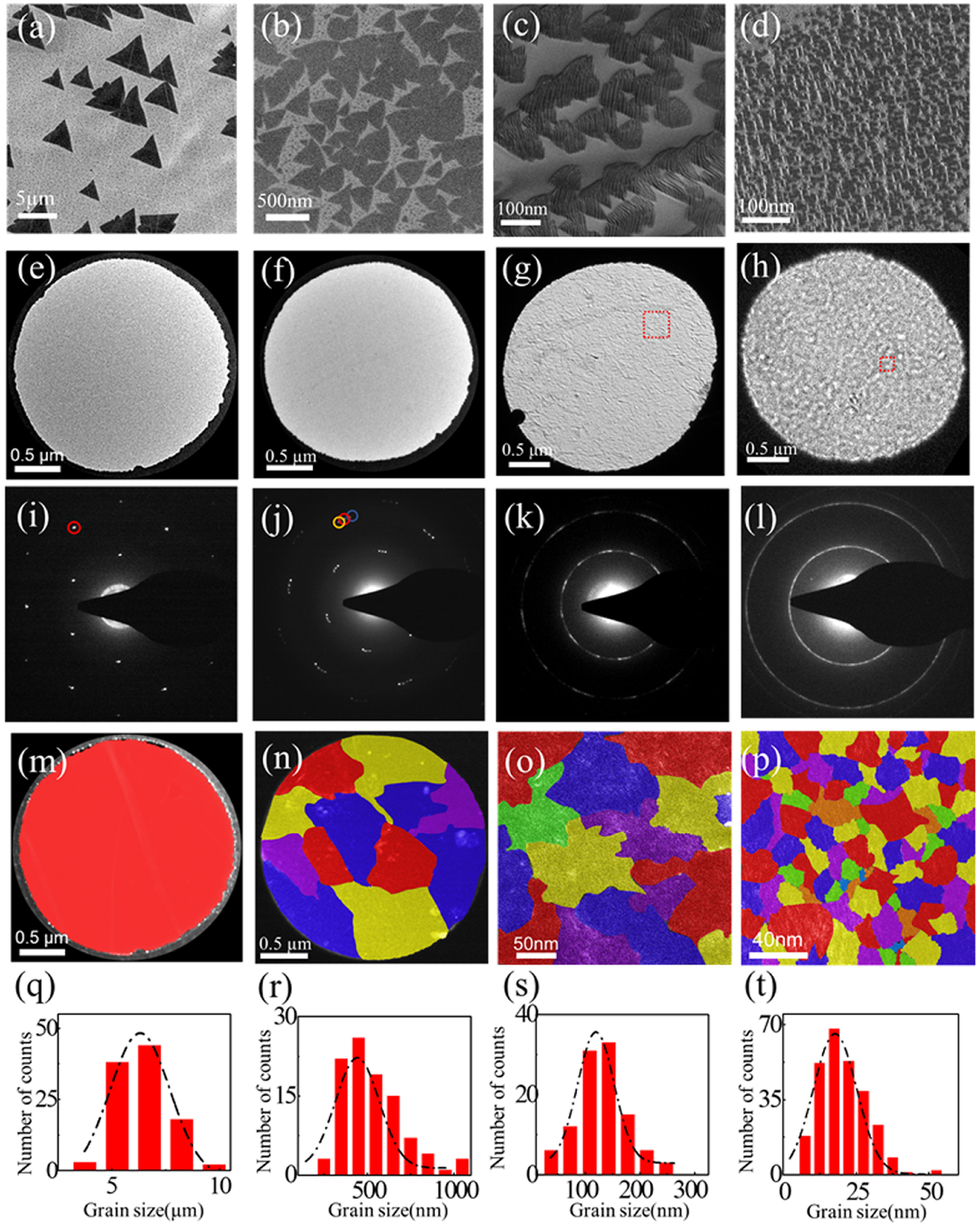
The large area monolayer h-BN films were synthesized on Pt foils, which was confirmed to have the superior catalytic property for conversion growth of h-BN under the same reaction compared with Cu and Ru substrates [23]. In order to obtain the desired h-BN domain size, various growth techniques based on CVD were applied. As shown in table 1, the Ni-foam assisted technique [24] that has been developed recently was applied to synthesize the large single-crystalline h-BN. The Cu enclosure technique [24] was utilized to obtain the h-BN with grain size up to ~500 nm. h-BN with grain sizes much smaller than ~150 nm were synthesized directly on Pt foil with the nucleation density engineered by the ammonia borane (AB) precursor heating temperature, which controls the precursor feeding rate. The key growth conditions were summarized in table 1 (see Experimental section for more details). Figures 1(a)–(d) illustrate the initial growth stages of the h-BN with grain sizes range from ~7 µm to ~20 nm. The fully covered poly-crystalline h-BN films could be achieved with extended growth time. The as-grown h-BN samples on Pt foil were then transferred onto the 90nm SiO2/Si substrates and the Au-coated holey silicon nitride (SiNx) substrates for further characterizations and opto-thermal measurement [25, 26] through a nondestructive bubbling-based transfer method (see supporting information, section 1 (stacks.iop.org/TDM/7/015031/mmedia)) [27]. The thickness of the four samples was measured by atomic force microscope (AFM, Bruker Dimension Icon) and the monolayer nature of the h-BN films was confirmed (see figure S1, in supporting information). Increasing surface roughness was observed with decreasing h-BN grain size, which is possibly due to the absorbed impurities or residues along the GB [28, 29] and the buckling of the h-BN sheet in the out-of-plane direction induced by the dislocations along the GB [30].
Table 1. Key Growth Conditions for CVD h-BN Specimens.
| Sample no. | A1 | A2 | A3 | A4 |
|---|---|---|---|---|
| Mean grain sizes | ~7 µm | ~477 nm | ~127 nm | ~19 nm |
| AB heating temperature | 75 °C | 75 °C | 75 °C | 90 °C |
| With Ni foam | Yes | No | No | No |
| With Cu enclosure | Yes | Yes | No | No |

Figure 1. (a)–(d) SEM images of the CVD h-BN specimens A1 to A4 with well-controlled grain sizes. (e)–(l) BF-TEM images (e)–(h) and the corresponding SAED patterns (i)–(l) of the suspended h-BN specimens on the holey SiNX substrates. (m) and (n) Corresponding false-color DF-TEM images of (e) and (f). (o) and (p) Corresponding false-color DF-TEM images of the dash red rectangle areas in (g) and (h). (q)–(t) Histograms of grain sizes with Gauss fit curve of the specimens A1 to A4.
Download figure:
Standard image High-resolution imageThe poly-crystalline nature of the as-synthesized h-BN films was confirmed by the diffraction-filtered imaging technique [31] based on the transmission electron microscopy (TEM, FEI Tecnai F20). To avoid damage to the h-BN samples, the TEM inspection was performed after the thermal measurement. Figure 1e to 1h show the bright-field TEM (BF-TEM) images of h-BN films with various grain sizes transferred onto the holey SiNx substrates, along with the selected area electron diffraction (SAED) patterns (figure 1(i)–(l)) acquired from the same region of the membrane. The electron diffractions from figure 1(e) show only one set of six-fold-symmetric spots (figure 1(i)), indicating the single-crystalline structure of h-BN for A1. Figure 1(j) contains a number of such families of spots, indicating that the field in Figure 1(f) contains multiple grains with different orientations. Using the objective aperture in back focal plane to collect electrons diffracted within a small range of angles [31] (marked by the color circles in figure 1(i)), the grain sizes of sample A2 can be clearly determined in the dark-filed TEM (DF-TEM) images by overlaying different colored patches with few-nanometers resolution. The complete maps of the grain structure, color-coded by the in-plane crystal orientation are shown in figure 1(n). Same processing has been performed on sample A3 and A4, except that the grain sizes in figures 1(g) and (h) are so small that only the electrons diffracted from a much smaller region (marked by the red squares in figures 1(g) and (h) form a diffraction ring. The corresponding color maps are shown in figures 1(o) and (p). The histograms of the grain sizes of the poly-crystalline samples (figures 1(r)–(t)) were eventually obtained by measuring hundreds of grains in each sample. The mean grain sizes estimated for A2, A3 and A4 were 477 ± 139 nm, 127 ± 35 nm, and 19 ± 8 nm, respectively. The histogram of grain sizes for A1 was obtained by collecting the h-BN grains of the initial growth stage obtained from the SEM images. Besides the grain size distribution, the BF-TEM images in figures 1(e)–(h) further verified the high quality of the suspended h-BN over the holes. No visible cracks were observed.
Figure 2(a) shows the optical micrograph of the suspended h-BN film on the Au-coated holey SiNx substrate with its strong asymmetric Raman E2g mode at ~1370 cm−1 clearly demonstrated in figure 2(b). Experimental work reported previously found it difficult to detect any Raman signal from the suspended monolayer and bilayer h-BN sheets grown on Cu foil by CVD [20]. However, both the pristine and the poly-crystalline h-BN films grown on the Pt foil exhibit clear and strong Raman E2g mode similar to mechanically exfoliated samples obtained from high quality h-BN crystals [22], and thus are suitable for further thermal measurement. Further comparisons of the Raman spectra of the suspended and supported h-BN grown on Pt foil and Cu foil were shown in figure S2. In addition, as shown in figure 2(c), the Raman E2g peak also show significant broadening of the full width at half maxima (FWHM) with smaller grain sizes indicating the increasing defect density [32]. The abrupt decline of the FWHM observed for sample A4 and A3 could be explained by the significant defect density difference due to the small laser irradiated region when doing Raman measurement under 100 × lens (the radius of the Gaussian laser beam is ~165 nm). Furthermore, Raman map of the E2g peak intensity clearly indicates the intactness of the suspended h-BN film over the holes (figure 2(d)).
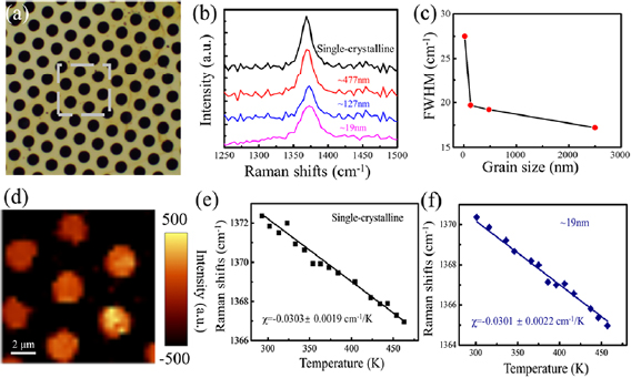
Figure 2. (a) Optical image of a monolayer h-BN film transferred onto the holey SiNx substrate. (b) The typical Raman spectra of the suspended monolayer h-BN with different grain sizes. (c) The FWHM of Raman E2g peak of the monolayer h-BN film as a function of grain size. (d) The corresponding Raman map of the dash rectangle area marked in (a). (e) and (f) Temperature dependence of Raman E2g peak frequency for monolayer h-BN with different grain sizes.
Download figure:
Standard image High-resolution imageThe opto-thermal Raman technique has been developed as an efficient method for the thermal conductivity measurement of 2D materials [25, 26, 33–35]. During the measurement, a 532 nm wavelength laser beam is focused on the center of the suspended h-BN using a 100 × objective lens. The absorbed power Q and the absorption coefficient were measured using a semiconductor laser power meter (supporting information, section 4). The temperature rise in the heated h-BN was determined from the shift in the Raman E2g peak [20]. The strong linear dependence of the Raman mode on the surrounding temperature has been reported in 2D layered materials such as graphene [25, 26], h-BN [20], and MoS2 [34, 35]. The extracted first-order temperature coefficients for the four samples (see both figures 2(e) and (f) and S3) were −0.0303 ± 0.0019 cm−1 K−1, −0.0296 ± 0.0034 cm−1 K−1, −0.0304 ± 0.0015 cm−1 K−1, and −0.0301 ± 0.0022 cm−1 K−1, respectively. No significant difference was observed. Figure 3(a) shows the relation between the measured temperature and the absorbed laser power for samples with various grain sizes when the laser beam was focused on the center of the suspended h-BN. The temperature rise of the single-crystalline samples is quite close to the sample with ~477 nm grain size but much smaller than that of the other two poly-crystalline ones, indicating the strong influence of the GB on the thermal transport of h-BN.

Figure 3. (a) The temperature measured at the center of the suspended h-BN versus the absorbed laser power for different grain sizes. (b) Thermal conductivity of the suspended monolayer h-BN with various grain sizes versus the measured temperature. (c) Thermal conductivity versus grain size with a nonlinear curve fit (red curve). (d) The inverse thermal conductivity versus inverse grain size with a linear fit (red line), whose slope is 0.104 ± 0.009.
Download figure:
Standard image High-resolution imageThe thermal resistance can be defined as  , where Q is the absorbed laser power, and
  is the temperature difference between the center of each suspended h-BN membrane (Thigh) and the substrates temperature (Tlow ~ 300 K) (supporting information, section 6). Owing to the small size of the samples (2.5 µm diameter) and the rapid measurement, the heat loss via convection can be ignored [36, 37]. For the case of diffusive phonons transport, the temperature distribution satisfies
and the thermal conductivity is [25]:
where R = 1.25 µm is the radius of the holes, t is the h-BN monolayer thickness (0.333 nm), and r0 = 0.165 µm is the radius of the Gaussian laser beam. The value of r0 was determined by performing micro-Raman scans across a smooth cleaved edge of a Si substrate [25, 26]. The α factor accounts for the Gaussian beam profile, which is 0.98 for the 100 × objective lens on the applied Raman system [25, 33].
The thermal conductivity κ of the h-BN with various grain sizes as a function of the measured central temperature Thigh was shown in figure 3(b). The experimental uncertainty considered consists of the Raman peak position temperature calibration, the temperature resolution of the Raman measurement method, and the uncertainty of the measured laser absorption [25, 26]. These individual uncertainties were incorporated into the overall uncertainty in κ via root-sum-square error propagation approach. As can be observed in figure 3(b), κ decreases over the entire temperature range with decreasing h-BN grain sizes. The κ of single-crystalline monolayer h-BN is the highest, ~544.6 ± 77.5 W m−1 K−1 at 315 K. This value is greater than those found in literatures for bulk [13], bilayer [6], and multilayer h-BN [19, 20], and agrees with the theoretical expectation for pristine monolayer h-BN very well [5]. The κ of ~477 nm, ~127 nm, and ~19 nm poly-crystalline h-BN are ~511.6 ± 71.2 W m−1 K−1 at 314K, ~310.2 ± 52.6 W m−1 K−1 at 320 K, and ~135.6 ± 22.4 W m−1 K−1 at 329 K, respectively. Due to the specifics of the experimental technique the results are given at similar but not exactly the same measurement temperatures.
It is worth noting that the poly-crystalline h-BN with grain size close to ~477 nm has similar κ with pristine single-crystalline h-BN (figures 3(b) and (c)). As shown by Jiang et al, at 300 K phonons with MFP shorter than ~450 nm comprise ~80% of the total in-plane κ for bulk h-BN, while 90% is comprised of phonons with MFP shorter than ~900 nm [38]. Here, the comparable κ experimentally observed between the single-crystalline h-BN sample and the poly-crystalline h-BN sample with grain size close to ~477 nm supports the concept that this grain size must be at least somewhat larger than the upper range of MFP for phonons that carry a significant fraction of the thermal energy. When the grain size was further reduced to ~127 nm and ~19 nm, far below the upper range of significant heat-carrying phonon MFPs in bulk h-BN, a substantial reduction of κ was observed down to approximately ~57% and ~25% of that for pristine h-BN.
The trend of the decreasing κ with increasing Thigh is indicative of increasingly strong anharmonic phonon scattering at higher temperature [25]. The negative dependence, however, gradually diminishes as the mean grain size (lg) decreases: κ ~T−2.22, κ ~ T−2.14, κ ~ T−0.47, κ ~ T−0.15 for lg = 7 µm, ~477 nm, ~127 nm, and ~19 nm, respectively. From kinetic transport theory, the MFP is determined by the anharmonic phonon Umklapp and the GB scattering. For the temperature range of this study where impurity/point defect scattering is of lesser importance (detailed discussion can be found in the supporting information, Section VII), the effective MFP can be estimated as  , where lph–ph and lg are the Umklapp limited and the GB-limited MFPs, respectively. While the Umklapp scattering has strong temperature dependence (follows the power law for temperature dependence of pure non-metallic crystals [39]) due to the increasing phonon populations at high temperatures, the GB scattering dependence on GB density or grain sizes is essentially independent of temperature. We can conclude that the boundary-phonon scattering gradually dominates the thermal transport with the increasing GB density, especially in the smallest grain size samples (~19 nm), where its κ is observed to have very weak temperature dependence to the point that it is within the uncertainty bounds of the measurement.
Figure 3(c) shows the κ of the h-BN films as a function of grain size (lg). The κ decreases exponentially from ~545 to ~136 W m−1 K−1 with the samples' change from single-crystalline to poly-crystalline with grain size ~19 nm at near room temperature. Analogous to 2D graphene, the heat flux in the poly-crystalline h-BN inclines to be perpendicular to the GB such that the global thermal resistance can be approximated as a series connection of local thermal resistances. Therefore, the thermal boundary conductance of GB can be estimated from [40–42]:

where G is the thermal boundary conductance, lg is the grain size, and κg is the thermal conductivity within a grain (~545 W m−1 K−1). As shown in figure 3(d), the plot of 1/κ versus 1/lg follows a linear line, whose extracted slope (0.104 ± 0.009) gives the value of the thermal boundary conductance G as 9.6 ± 0.8 GW m−2 K−1, which agrees with the value predicted via the finite element approach (11 ± 1 GW m−2 K−1) [14] very well.
To understand the role of the grain size on κ in depth, we conducted a series of MD simulations on 2D circular h-BN thin films. Figure 4(a) shows the configuration. The heat flux is introduced from a hot bath (colored in red) with a high temperature (Thigh) to the cold bath (colored in blue) with a low temperature (Tlow). Tlow and Thigh are fixed to 300 K and 400 K. The geometries and setups simulate those in our experiments, and the applied Thigh and Tlow are also close to the experimental values. Details on the methods employed can be found in the supporting information (section 8).

Figure 4. (a) The MD simulation schematic diagram, R = 800 Å. (b) and (c) Spatial temperature distributions for single-crystalline (b) and poly-crystalline monolayer h-BN (c). The black dotted lines in (c) denote the GB. (d) Radial distribution of the rescaled temperature, (T − Tlow)/(Thigh − Tlow), in the single-crystalline (red triangles) and the poly-crystalline (blue triangles) monolayer h-BN. The black dash line shows the boundary of the hot bath. (e) and (f) The radial temperature profiles of white dash lines in (b) and (c), respectively. Basically, where there is a GB in (c) there is correspondingly a temperature jump in (f). (g) PPS of B and N atoms in single-crystalline h-BN. (h) and (i) PPS of two representative pairs of B and N atoms along/near GB in poly-crystalline h-BN.
Download figure:
Standard image High-resolution image
The temperature distributions in single-crystalline and poly-crystalline h-BN are plotted in figures 4(b) and (c), respectively. The temperature is distributed quite evenly and axisymmetric in the single-crystalline h-BN case. The obtained temperature distribution within the poly-crystalline h-BN case, however, is much different. It can be clearly observed that the isotherm curves incline to be along the GB, reflecting the high thermal resistance that the heat undergoes when it flows across the GB. The temperature profiles along the white dashed lines in figures 4(b) and (c) are plotted in figures 4(e) and (f) for comparison. Sharp discontinuities in temperature at the GB are apparent in the poly-crystalline h-BN system. The rescaled temperature (T − Tlow)/(Thigh − Tlow) versus the rescaled radius r/R in single logarithmic plot is shown in figure 4(d). According to equation (1) such a profile should be linear when plotted on such axes, provided that the thermal conductivity is geometry- and temperature- independent. It is approximately true for the poly-crystalline case, in spite of the large fluctuations. For the single-crystalline system, however, the profile displays noticeably different behavior. Such a nonlinearity when plotted on such axes should not be attributed to the negative temperature dependence of κ, because this dependence is very small. More importantly, the deviation from the profile predicted in equation (1) persists even when a much smaller temperature difference (with Tlow and Thigh fixed to 330 K and 370 K) is applied. It is in fact mainly related to the system boundary conditions [43]. The singularity-like temperature profile has also been found in graphene [42] and some one-dimensional lattice models [43]. Such a nonlinearity is basically invisible in the poly-crystalline cases, indicating the strong scattering of phonons by GB that largely decreases the MFP. Therefore, any long-range effect is greatly reduced and consequently the thermal conductivity is reduced significantly in poly-crystalline systems [44].
To further understand the physical underlying mechanism for the high thermal resistance at the GB, the phonon power spectra (PPS) of some atoms are calculated. The PPS of N and B atoms in a single-crystalline h-BN are shown in figure 4(g), which are similar to those in the previous reports [14, 45]. The PPS of the two kind of atoms match each other very well, in particularly in the low frequency regime in which phonons carry heat the most efficiently. As a result, the thermal conductivity is thus quite high. For the poly-crystalline systems, the vibration of atoms along/near GB becomes more complicated and disordered. As shown in figures 4(h) and (i), the match of their PPS is much poorer, which implies much stronger scattering of phonons and accounts for the much shorter phonon MFP. The detailed method and PPS for additional atoms can be found in the supporting information (section 8).
The match of phonon PPS can be measured quantitatively by [46]:
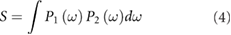
where the P1(ω) and P2(ω) denote the PPS of two atoms. The very strong relevance between S and thermal resistance has been presented in [46]. The S value of the single-crystalline h-BN system is approximately 59, but for the selected two cross-GB pairs of atoms in the poly-crystalline system S equals only 23 and 25, respectively, which indicates much lower matching and, as a result, much lower thermal conductivity [46].
3. Conclusions
In summary, the thermal conductivity of monolayer h-BN with mean grain sizes ranging from ~19 nm to single-crystalline was investigated by employing a noncontact technique based on micro-Raman spectroscopy. The κ of the pristine monolayer h-BN measured is ~545 to ~286 W m−1 K−1 for temperature ranging from ~315 K to ~412 K. The poly-crystalline h-BN with mean grain size of 477 nm, which is close to the upper limit of heat-carrying phonon MFPs, exhibit comparable κ value to the pristine h-BN in the entire temperature range examined. These results indicate strong potential for CVD grown poly-crystalline h-BN sheets in thermal management applications due to its much lower manufacturing difficulty in comparison to that of the pristine single crystal h-BN. When the grain size reduces to ~19 nm, the measured κ decreases prominently to ~136 W m−1 K−1 and becomes insensitive to the temperature changes, suggesting that boundary-phonon scattering becomes dominant over the intrinsic phonon-phonon scattering. The grain size effect has been further studied by MD simulations. The results confirm the major contribution of GB in the poly-crystalline h-BN systems. The disordered vibration spectra of atoms along/near the GB results in the mismatch of PPS, which greatly enhances the phonon scattering. The phonon MFP is thus distinctly shortened and consequently the κ is greatly reduced. These findings not only are important for establishing a comprehensive understanding of the phonon transport properties of h-BN and other emerging 2D materials, but also encourage the grain boundary engineering of CVD synthesized 2D materials for tunable thermal conductivity aiming for practical applications.
4. Experimental section
4.1. Synthesis of monolayer h-BN films of different grain sizes
The single-crystalline monolayer h-BN samples were synthesized on the Pt foils by using the Ni foam assisted technique [24]. The substrate (a Pt foil inserted into a Cu enclosure together with the Ni foam on the upstream) was placed in the reaction zone. The growth of h-BN was performed at 1050 °C with the AB precursor heated up to 75 °C, and the H2 flow was kept at 10 sccm during the whole growth process. Figure 1(a) shows the typical h-BN grains after growth for 30 min. Figure 1(b) shows the h-BN grains of ~477nm by removing the Ni foam from the Cu enclosure while keep other growth conditions consistent. The fully covered film was obtained with the growth time extended to 40 min. The samples with mean grain sizes of ~127 nm and ~19 nm were achieved directly on Pt substrate with AB heating temperatures of 75 °C and 90 °C, respectively. The growth time for figures 1(c) and (d) were both 1min. Full layer h-BN could be achieved by extending the growth time to 5 min.
Acknowledgment
We appreciate the support from the National Natural Science Foundation of China (11374244, 11675262, 11774032 and 51571035), from Beijing Natural Science Foundation through grant (2192024 and 1192010), from the Fundamental Research Funds for the Central Universities, and the Research Funds of Renmin University of China (No. 17XNLF02), and from the FANEDD through grant No. 201443. Computational resources were provided by the Physical Laboratory of High-Performance Computing at Renmin University of China.
Supplementary material
Additional information on the transfer of the suspended monolayer h-BN films, AFM characterizations, details of thermal measurements and numerical simulation are shown in supporting information.