

Abstract
Superlattice engineering provides the means to reshape the fabric felt by quasiparticles moving in a material. Here we argue that bandstructure engineering with superlattices can be pushed to the extreme limit by stacking gapped van der Waals (vdW) materials on patterned dielectric substrates. Specifically, we find that high quality vdW patterned dielectric superlattices (PDS) realize a series of robust flat bands that can be directly switched on and off by gate voltage in situ. In contrast to existing superlattice platforms, these flat bands are realized without the need for fine tuning. Instead, the bands become flat as the gate voltage increases in magnitude. The characteristics of PDS flatbands are highly tunable: the type of flatband (single non-degenerate or dirac-cone-like), localization length, and interaction energy are sensitive to the applied gate voltage. As a result, electron-electron interactions in the PDS flatbands can become stronger than both the bandwidth and disorder broadening, providing a setting for correlated behavior such as flatband ferromagnetism. We expect PDS flatbands can be experimentally realized in a range of readily available gapped vdW materials such as monolayer transition metal dichalcogenides, e.g. WSe2.
Export citation and abstract BibTeX RIS

Original content from this work may be used under the terms of the Creative Commons Attribution 3.0 licence. Any further distribution of this work must maintain attribution to the author(s) and the title of the work, journal citation and DOI.
Van der Waals (vdW) heterostructures have become a powerful platform to tailor the electronic properties of materials [1–3]. One case in point is moiré superlattices, formed when two vdW materials are stacked and twisted. In such moiré materials, electrons and other quasiparticles experience slowly varying (emergent) effective periodic potentials. Even when the potentials are relatively weak (as compared with the kinetic energy of electrons in each layer), a wide variety of phenomena can be realized that include for e.g. emergent electronic bandgaps [4], moiré excitons [5–9], Hofstadter spectra [4, 10, 11], topological bands [12, 13], as well as a magnetic proximity effect [14] to name a few. However, when top and bottom layers couple strongly, extreme bandstructure reconstruction takes effect, allowing nearly flat electronic bands to form at magic [15, 16] or low-twist angles [17, 18]. These provide a vdW venue to realize correlated behavior, with intense interest sparked by reports of correlated insulating behavior and superconductivity in moiré materials under such conditions [19–21].
However, achieving good twist angle control over moiré supelattices can often be experimentally difficult; this can be further complicated by lattice reconstruction that arise at low twist angle [22]. Good twist/registration control becomes critical given that extreme bandstructure engineering typically occurs only at specific 'magic' twist angles or in a small range of low-twist angles [15–18]. Recently, an inverted electrostatic strategy—patterned dielectric superlattices (PDS)—wherein a dielectric material is patterned into a superlattice and placed on top of a gate electrode (figure 1(a)) has been experimentally demonstrated in graphene [23], producing high quality superlattices. In these, dielectric contrast between patterned hole and dielectric substrate material enables the gate electrode to sustain a spatially modulated superlattice potential (figure 1(b)). Perhaps most remarkable is that the PDS devices maintained an ultrahigh mobility (where the patterned dielectric did not significantly degrade the device performance [23]), as well as high gate electrode tunability that could turn electrically on and off the superlattice potential.

Figure 1. (a) Schematic of a triangular patterned dielectric superlattice (gray) and the spatial potential profile (purple) sustained for the target gapped van der Waals material (red). Here the top gate (yellow) and back gate (blue) sustain a potential drop in the out-of-plane direction. The spacing between two neighboring holes is a. (b) Electrostatic potential for a single hole inside the dielectric substrate (gray) in between top and bottom gates, see SI for full details. The top panel shows the electric potential across the red line (plane of the vdW material) displayed in the bottom panel. Thin white lines indicate equi-potential contours. Here we have used a potential difference between the two (top and bottom) gates of  for illustration giving a superlattice potential amplitude (
 see equation (1)) of about 12.5 meV; we note these correspond to electric fields smaller than the dielectric breakdown voltage of hBN. While here we have chosen a specific value of a for illustration, flat minibands occur generically for other a, see text.
Download figure:
Standard image High-resolution imageHere we argue that PDS can be pushed into the strong coupling regime, where the superlattice potential ( ) can exceed the kinetic energy of the electrons in a gapped vdW material. As we describe below, in this regime, flat electronic minibands can be achieved and are highly gate-tunable. Strikingly, these flatbands do not require fine tuning of twist angle. Indeed, the bands become flat as gate voltage is switched on, achieving small bandwidths even for modest superlattice potentials (figure 2); as shown below, flat minibands occur generically for other superlattice periods a chosen. These stand in contrast to strategies using moiré superlattices that only feature flat bands at magic or low twist angles [15–18].
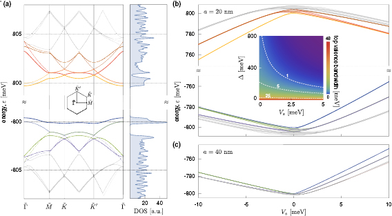
Figure 2. (a) Superlattice miniband dispersion (left) and the corresponding density of states (right) for vdW PDS with monolayer WSe2. Here the electronic structure is described by equation (1) with  ,
,  ; the substrate is a triangular patterned dielectric superlattice with
  (see figure 1(a)). Solid (dashed) lines are for
  (
( ) (see equation (1)), and the inset shows the mini Brilluoin zone defined by the superlattice. (b) Miniband minima and maxima that indicate its bandwidth are plotted as a function of
  for 12 mini-bands close to the intrinsic band gap. Here solid colored lines indicate miniband maxima and minima, whereas shaded region indicate region in between maxima/minima in the minibands. All other parameters (aside from varying
  ) are the same with those in (a). The inset shows the top valence bandwidth as a function of
  (with
(with  and a fixed to the values indicated in (a)). (c) Similar to (b), but only showing valence minibands with
  revealing gate-tunable flat minibands.
Download figure:
Standard image High-resolution imagePDS flatbands can be achieved in gapped vdW materials such as the transition metal dichalcogenides. The key ingredients are a large bandgap as well as a large effective mass. The former ensures that conduction and valence bands do not cross when  is applied, and the latter gives a small initial kinetic energy of the electrons. These enable the superlattice potential to confine the electrons effectively and form flat minibands. A particularly good candidate for PDS flatbands is WSe2, wherein high mobility (
 cm2 Vs−1) samples have been isolated [24]; these have mean free paths of several hundred nanometers, see supplementary information, SI3; electrons in such samples can Bragg scatter off the superlattice potential many times. For WSe2, we anticipate flat electronic minibands that are well separated can be achieved for modest
  and superlattice periods. Interestingly, PDS yields bunches of flat bands that proliferate throughout the parameter space. For example, for
  , we find that in addition to the top most valence miniband which is a single non-degenerate flatband (per valley), the other lower (valence) minibands also bunch up into flatband bundles. Similar flatband bundles can be found for
  , as well as in the conduction band.
Perhaps the most exciting aspect of PDS flatbands is the possibility of direct gate access to correlated behavior. As an illustration, we consider ferromagnetism in a PDS flatband; this is in close analogy with quantum-hall ferromagnetism. In such a case, we find a ferromagnetic state, where the spins in either valley  are favored, can be achieved for readily available samples and superlattice gate voltages.
Gate tunable flat minibands
We begin with a discussion of the PDS scheme using monolayer transition metal dichalogenides (TMD). The PDS that we consider here (and that can be experimentally fabricated) are of fairly long-wavelength  . The resulting superlattice bandstructure can be captured by an effective
  model expanded close to the K and
  points as

where  is the velocity,
  are the Pauli matrices,
  is the bandgap of the TMD,
  for K and
  valleys,
  is the amplitude of the superlattice potential applied by the PDS scheme in figure 1, and
 ![$ \newcommand{\re}{{\rm Re}} \renewcommand{\vec }[1]{{\bf #1}} f(\vec {r})$](https://content.cld.iop.org/journals/2053-1583/7/1/015028/revision1/tdmab59a8ieqn030.gif) is the spatial pattern of the superlattice potential. Here we have suppressed spin indices since the bandstructure physics we discuss does not differentiate between spin/valley species (i.e. the superlattice potential is a scalar potential); spin can be included in a straightforward fashion that does not affect the physics we discuss below. Further, we note that the particularly large Ising spin splitting (∼ hundreds of meV) in the valence bands of many TMD materials, effectively lock the valley and spin in the valence bands making the model in equation (1) a good descriptor of the low-energy mini-bandstructure.
is the spatial pattern of the superlattice potential. Here we have suppressed spin indices since the bandstructure physics we discuss does not differentiate between spin/valley species (i.e. the superlattice potential is a scalar potential); spin can be included in a straightforward fashion that does not affect the physics we discuss below. Further, we note that the particularly large Ising spin splitting (∼ hundreds of meV) in the valence bands of many TMD materials, effectively lock the valley and spin in the valence bands making the model in equation (1) a good descriptor of the low-energy mini-bandstructure.
As shown in figure 1(b), dielectric inhomogeneity in the substrate material can enable electric control of a spatially inhomgeneous potential with variations on the order of the hole width (e.g. several tens of nanometers) [23]. Here gray indicates a dielectric (shown SiO2 with  ) and empty indicates air (
 ). As shown, when a gate potential is applied, the dielectric contrast yields a spatially modulated potential even in the vdW material layer (red) with potential amplitudes
  that can be switched on and off electrically [23]. Figure 1(b) was plotted using a numerical solution for a generalized Poisson equation in a spatially inhomogeneous dielectric environment (see supplementary information, SI (stacks.iop.org/TDM/7/015028/mmedia)).
To illustrate the (flat) band structure engineering in the PDS of vdW materials, we first use a triangular superlattice (see other lattices in SI) so that
where ![$ \newcommand{\re}{{\rm Re}} \renewcommand{\vec }[1]{{\bf #1}} \vec {G}_i$](https://content.cld.iop.org/journals/2053-1583/7/1/015028/revision1/tdmab59a8ieqn034.gif) are the triangular superlattice wave vector oriented
are the triangular superlattice wave vector oriented  relative to each other,
 ![$ \newcommand{\p}{\partial} \newcommand{\re}{{\rm Re}} \renewcommand{\vec }[1]{{\bf #1}} |\vec {G}_i| = 2\pi/a$](https://content.cld.iop.org/journals/2053-1583/7/1/015028/revision1/tdmab59a8ieqn036.gif) , and
, and  is a relative phase. For simplicity, we will set
  in the following. It does not qualitatively affect the physics we discuss below. As expected, the superlattice folds the original TMD bands into a series of superlattice minibands (band folding is illustrated for
  as the light dashed lines in figure 2(a)). Here the bandstructure is plotted in a superlattice defined mini Brilluoin zone (MBZ), where the tilde symbol indicates the MBZ. When
  is switched on, Bragg scattering mixes the bands and produces a mini-band structure (colored lines and gray lines with
  ) in both the conduction band (positive energies) and the valence band (negative energies) as shown in figure 2(a). We have colored only the first three conduction and valence minibands so as to focus our discussion on them; in solving for the mini-bandstructure a set of 162 mini-bands are employed to ensure convergence of the lower bands (we only show 12 minibands) that we focus on in the main text. Physically, the inclusion of many minibands in our numerical calculation is to capture the physics of the extreme bandstructure reconstruction regime in which the superlattice strength
  is larger than that of a kinetic energy of the electrons. Here we have used material parameters corresponding to WSe2 with
  ,
,  [26].
[26].
Strikingly, a clear gap between the top most (valence) miniband (blue, figure 2(a)) and the rest of the minibands opens up. This is distinct from that expected from graphene PDS [23] where a  berry phase prevents backscattering and gap opening; in the case of graphene PDS secondary Dirac cones form at the MBZ corners [4, 10, 11, 23, 25]. In contrast, the wavefunction (AB-sublattice pseudospinor) in TMD close to the band edge has weight mostly on a single sublattice (aligned to a pole in the Bloch sphere), allowing maximal backscattering and mini-gap formation.
Due to the large  in TMDs, minigap opening squeezes the top most valence miniband creating a confined energy window for it to exist with a sharp density of states (shaded blue in right panel of figure 2(a)). Indeed, as
  is increased, the top most (valence) mini-band is further flattened (figure 2(b)) with very narrow band-widths (
 ) achievable with modest applied gate voltage creating a nearly flat band. To see this, we have plotted the maximum and minimum energy in each miniband (solid lines figure 2(b), this indicates the bandwidth) with the colors used corresponding to the colored 3 conduction and colored 3 valence minibands of figure 2(a); the shaded region between miniband maxima and minima are shaded in corresponding colors. We note that the flat top most (valence) miniband is well separated from other bands with the large
  to the minibands in the conduction band, and gate tunable minigaps to the other minibands in the valence band (that can reach tens of meV); the minigaps increase with applied gate potential, see SI.
One unusual feature is that the application of superlattice PDS also renormalizes the effective bandgap between the conduction and valence band states, with changes in effective bandgap of up to  for the largest superlattice potential amplitude shown in the figure (see figure 2(b)). This arises from the significant miniband reconstruction. Indeed locally in real space, the electrons feel large variations in superalattice potential that range from
  at the peak to
  in the troughs. This large peak-to-trough difference enables electrons to be confined locally to produce a flatband structure (figure 2(a)).
The blue band is not the only flat band that occurs in PDS. For example, at sufficiently high superlattice potential ( ), both green and purple minibands in the valence band flatten out. Unlike the blue band they tend to stick together. In fact, the PDS scheme yields sets of flat minibands in the valence band (some of which are nearly degenerate with each other forming bunched bundles of bands) with severely compressed bandwidths. Each of these bundles of flat bands are well separated from each other with large electrically tunable minigaps (in figure 2(b), we show three flat miniband bundles in the valence band at
  ).
).
We note that the PDS scheme, when applied to gapped Dirac materials such as WSe2, naturally breaks particle-hole symmetry with (positive and negative energy) minibands exhibiting contrasting behavior (see figure 2(a)). For example, when  the top (valence) miniband (blue) gets squeezed into a single non-degenerate flat miniband and is well separated from the other minibands, while the bottom (conduction) miniband (yellow) adheres closely to the next miniband (red); this displays a particle-hole asymmetric behavior. Symmetry in the miniband structure, however, is restored when both
  and
and ![$ \newcommand{\re}{{\rm Re}} \renewcommand{\vec }[1]{{\bf #1}} \varepsilon_{\vec {k}} \to - \varepsilon_{\vec {k}}$](https://content.cld.iop.org/journals/2053-1583/7/1/015028/revision1/tdmab59a8ieqn058.gif) are interchanged (see detailed discussion in SI).
are interchanged (see detailed discussion in SI).
This unconventional feature allows the type of flat mini-bandstructure to be tuned by gate voltage. When  the top (valence) miniband (blue) is a single non-degenerate flat band (per valley). However, when
  this same blue miniband, while flattening out, adheres closely to the green band (figure 2(b)); when large enough gate voltage is applied, they form a close pair of flatbands that bunch together. This flatband bundle has a width
 . Even though both green and blue minibands stay together, nevertheless, we find that they are separated by a very small energy gap. Indeed, close to
  points, the blue and green miniband structure (for
  ) bands resemble Dirac cones (with an extremely small gap; we estimate the gaps to be of order several
  , see SI). We note that away from the small minigaps, the miniband spectra mimic the flattened Dirac bands in twisted bilayer graphene [15]; interestingly, the chirality of electrons at
  points are the same (see SI) mirroring the behavior found in twisted bilayer graphene.
As a result, PDS enables to achieve multiple types of flatbands via in situ gate voltage tuning (e.g. from single non-degenerate flat-miniband for positive  to Dirac-cone-like for negative
  ). This unusual asymmetric behavior (for both conduction/valence bands and opposite signs of
  ) arises from the gapped Dirac pseudo-spinor form of their wavefunctions (such asymmetry does not arise for a simple massive two-dimensional electron gas). Indeed, the role of the TMD pseudospinor texture is further evidenced by how PDS induced Bragg scattering also changes the winding of the gapped Dirac pseudo-spinor wavefunctions. This dramatically reconstructs the Berry curvature distribution in each of the minibands (for discussion of miniband Berry curvature, see SI).
One of the most attractive features of PDS flat bands, is that they do not occur at fine-tuned gate voltages or superlattice wavelength. The larger the superlattice wavelength, the smaller the applied superlattice potential needed to flatten the PDS minibands (see for e.g. figure 2(c) where a larger superlattice wavelength  was used). Indeed, the main requirement imposed on the superlattice wavelength is that it should be smaller than the sample (disorder) mean free path to enable the electrons to Bragg scatter off the superlattice potential (see SI for an estimate of the mean free path of WSe2). Further, even when an intrinsic conduction and valence band mass asymmetry is included in the bare TMD hamiltonian, we find that the flat minibands remain robust, with only small changes in their miniband dispersion relation, see full discussion in SI. This PDS strategy stands in stark contrast to the flat bands found in moiré superlattices where specific 'magic' twist angles between layers are required (in the case of twisted bilayer graphene) or low twist angles required in other moirè superlattice strategies.
Instead, the key to achieving flat bands in PDS is large  as well as low velocities. As shown in the inset of figure 2(b), when we fix
  and a (same parameters as panel (a)), the larger the
  , the smaller the bandwidth at a given superlattice potential
  . For WSe2, we find
  allowing very small bandwidths to be achieved even for small
  applied, e.g. the bandwidth is ∼
 when
when  . We note, parenthetically, that when
  is small so that
  applied is on order
  , the minibands in the conduction and valence band can start to mix, vastly complicating the miniband structure and making the conditions for flat bands in PDS hard to achieve.
We anticipate that the PDS scheme can be applied to other van der Waals materials with large bandgaps. For example, we have computed the miniband structure for a range of TMD materials and have found that well separated sets of flat minibands generically occur—see SI for full band structure. Further, other superlattices can also be easily implemented and produce qualitatively the same results: we have computed the minibands for square as well as hexagonal superlattices as well and find similar well separated sets of flat minibands, see SI. This versatility with superlattice structure provides the ability to study flatbands and its concomittant interaction effects in other types of lattices which can have a different type of symmetry (that may be different from the underlying lattice).
Flatband ferromagnetism
Perhaps the most striking consequence of PDS flat bands is the ability to enhance correlation effects. This is because the extremely small bandwidth of single-particle mini-bandstructure of PDS (
 ) quenches the kinetic energy of the electrons. As a result, other energy scales such as that arising from electron-electron interactions can determine the behavior of the electronic system. For clarity, in the following, we will focus on the top-most valence miniband for
  which is well separated from the other superlattice minibands. Further, we note that due to the large Ising splitting in TMDs, the spin and valley degree of freedom are locked; at the non-interacting level, this band has only a two-fold degeneracy with spin up and spin down occurring in the (original) valleys at K and
  .
.
To proceed, we first estimate the strength of electron-electron interactions in the superlattice by modeling the average interaction energy of electrons confined in the troughs of the superlattice potential as [27, 28]
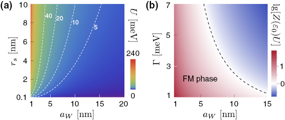
where  is the effective inverse screening length, and aW is the extent of the PDS flatband electronic wavefunction confined in the troughs of the superlattice. Here we have chosen a simple Gaussian ansatz for the extent of the wavefunction; other models do not qualitatively affect the results we discuss below. In figure 3(a), we plot the strength of U as a function of both the screening length rs as well as aW taking
  . This yields large interaction energies of order several tens of meV for a wide range of rs and aW. For WSe2, we estimate effective rs of a few nanometers arising either from intrinsic screening of the electron gas or from proximal gates, see discussion in SI. To estimate the extent of the electronic wavefunction aW, we employ a variational approach on the Gaussian wavefunction ansatz. This yields typical aW that decreases for increasing superlattice potential, reaching a fairly confined state of ∼5–10 nm even for modest applied superlattice potential, see SI.
Figure 3. (a) Interaction energy U as a function of the extent of electronic wavefunction in the flat band, aW, and effective screening radius, rs. Dashed contour lines indicate lines of constant U and are in units of meV. (b) Dimensionless  , see equation (5) indicating propensity for the ferromagnetic instability with
 ![$ \newcommand{\p}{\partial} Z(\mu_0=\varepsilon_0) = [ \sqrt{2\pi \Gamma^2} ]^{-1}$](https://content.cld.iop.org/journals/2053-1583/7/1/015028/revision1/tdmab59a8ieqn089.gif) and taken at a fixed
and taken at a fixed  for illustration. For
  (boundary denoted by dashed line), the system enters a ferromagnetic instability. Here lg denotes
  .
.
Download figure:
Standard image High-resolution image
Figure 3(a) indicates that U can dominate over the extremely small non-interacting PDS flatband bandwidths (see e.g. figure 2). As a result, we anticipate interaction effects can become significant. For example, adopting a Hartree–Fock approximation, we find that the exchange integral (i.e. the Fock-part of the electron self-energy for the bands) can be large and drive the spin-degenerate flatband system into a Stoner-type ferromagnetic state [28]; the exchange integral can be estimated by U in equation (3) following [27, 28]. To describe this, we use a simple mean-field model for the energy density  of a PDS flat miniband with spins indexed
  as
as
where  is the chemical potential of spin s, and
  is the band energy, and U can be estimated by equation (3) (for a full description, see SI). Here we have used a simple Gaussian
 ![$ \newcommand{\e}{{\rm e}} Z(\varepsilon) = A \exp [ - (\varepsilon - \varepsilon_0){}^2 / 2\Gamma^2 ]$](https://content.cld.iop.org/journals/2053-1583/7/1/015028/revision1/tdmab59a8ieqn097.gif) to model a broadened spectral weight of the flatband, and the density of each spin species is
to model a broadened spectral weight of the flatband, and the density of each spin species is  . The broadening,
  , can be induced by a number of different processes for e.g. via disorder. Other forms of the spectral function do not affect the qualitative conclusions we discuss below. Here
 ![$ \newcommand{\p}{\partial} A = [ \sqrt{2\pi \Gamma^2} ]^{-1}$](https://content.cld.iop.org/journals/2053-1583/7/1/015028/revision1/tdmab59a8ieqn100.gif) is a normalization constant.
is a normalization constant.
For small U, the two spin species are degenerate with  is the spin chemical potential. However, for large enough U this spin symmetry can become broken. To see this, we first write
  where
where  . Expanding equation (4) to
  we obtain the energy density for the flatband as

where  is the energy in the symmetry unbroken phase, and the
  term describes the energy cost to imbalance the spin species. Crucially, an instability in the spin up/down population is induced when the coefficient of the second term is negative
  ; this is analogous to the Stoner criterion that has been successfully applied to understanding quantum Hall ferromagnetism [28].
The conditions for symmetry breaking depend on a competition between the broadening and U. In our model above, this is parameterized by rs, aW, as well as the broadening energy/width  . To illustrate this, we plot
  in figure 3(b). From figure 3(b), we can see the competition clearly: for larger (smaller)
  , we require more (less) localized electron states, or larger (smaller) U to enter the broken symmetry phase. Taking
  as a demonstration, we find large
  for wide swathes of the
  -aW parameter space (figure 3(b)). We estimate that
  –
– can be achieved by modest superlattice potentials in the PDS scheme. At low temperatures, broadening is typically dominated by disorder [29–31]. Taking values for high quality WSe2 [24], we estimate disorder-induced broadening
  of order several
  are available in high quality present day samples, see SI. As a result, we expect that the conditions for realizing a ferromagnetic state using PDS flatbands can be attained in WSe2. Interestingly, this analysis is not confined to
  . The ferromagnetic instability can occur at a variety of chemical potentials so long as the criterion is satisfied
  , see below.
Discussion
There are numerous probes of the extreme mini-bandstructure reconstruction we discuss here. For example, we anticipate a lightly hole doped WSe2 PDS to exhibit a dramatic change in its low-frequency (THz) optical absorption characterisitcs as  is switched on. While at
  such a sample will exhibit a Drude peak around
  , when
  is switched on, the Drude peak will diminish as the topmost (valence) miniband flattens, and exhibit additional sharp THz absorption peaks corresponding to transitions between the sets of flat minibands (in the valence band).
Similarly, we expect dual-gate control to enable control of both superlattice potential as well as the filling of the minibands. Such filling control can enable to probe both the metallic as well as the insulating states induced by the superlattice potential. When pushed into the regime where flatbands exhibit ferromagnetism, the spins (locked to the valley) split; at  the flatband would exhibit a ferromagnetic insulating state. Interestingly, ferromagnetism can also occur away from
  so long as
  . As a result, the ferromagnetic system can be metallic. Crucially, we note that the minibands exhibit non-zero Berry curvature distribution (see details in SI). As a result, when the spins/valleys are split we anticipate that a (charge) anomalous Hall effect can ensue.
In summary, PDS in gapped vdW materials provide a venue to realize flatbands without the need for sensitive twist angle alignment or stacking arrangement. Instead, extreme bandstructure engineering arise directly from gate-controlled superlattice potentials yielding flatbands when gate voltage is applied; when gate bias vanishes, the PDS system remains as an ordinary TMD system. As a result, PDS flatbands afford considerable electrical control over the character of their electronic excitations (e.g. miniband-width, miniband-gap, interaction energy), as well as an on/off switch for flatbands. While we have focussed on ferromagnetic ordering, highly localized electrons can also exhibit other types of magnetic ordering including antiferromagnetic order as well spin liquids (for a recent discussion see e.g. [17]); having two extremely flat bands separated by a small gap may provide a possible venue for unusual excitonic correlations [32]; a large local density of states may enhance pairing and unlock superconducting correlations. Lastly, we note that the PDS scheme can offer access to a variety of other mini-bandstructures. For example, in addition to a scalar superlattice potential that we focus on to illustrate PDS flatbands, in low-symmetry 2D materials (e.g. monolayer 1T'-WTe2) spin–orbit coupling can be readily controlled by gate voltage [33, 34] enabling a spatially modulated spin texture; this spatial spin texture can be used as a further knob to control spin response. Another example arises from how the large changes in the local dielectric environment can induce gap size variations in real space [35]; these may give rise to a  superlattice potential. Given the large variety of available superlattice structures that can be patterned using PDS, the characteristic length scales for PDS (several tens of nanometers), as well as the exposed nature of the surface states, such heterostructures may provide a one-stop platform to realize and spatially probe exotic ordering.
Acknowledgments
We are grateful for useful conversations with Valla Fatemi, Ataç Imamoğlu, Brian Skinner, Javier Sanchez–Yamigishi, and Noah Yuan. This work was supported by the Singapore National Research Foundation (NRF) under NRF fellowship award NRF-NRFF2016-05, a Nanyang Technological University start-up Grant (NTU-SUG), and Singapore MOE Academic Research Fund Tier 3 Grant MOE2018-T3-1-002.
Footnotes
- 3
The supplementary information contains a detailed discussion on the superlattice band structure, Poisson's equation and electric potential generated using PDS scheme, particle-hole asymmetry, Berry curvature in the reconstructed minibands, PDS induced minigaps, other types of superlattices and the PDS scheme in other TMD materials, estimate for disorder broadening, mean free path, extent of the electronic wavefunction, and derivation of the effective model for flatband ferromagnetism.