
Abstract
Atomically thin semiconductors hold great potential for nanoscale photonic and optoelectronic devices because of their strong light absorption and emission. Despite progress, their application in integrated photonics is hindered particularly by a lack of stable layered semiconductors emitting in the infrared part of the electromagnetic spectrum. Here we show that titanium trisulfide (TiS3), a layered van der Waals material consisting of quasi-1D chains, emits near infrared light centered around 0.91 eV (1360 nm). Its photoluminescence exhibits linear polarization anisotropy and an emission lifetime of 210 ps. At low temperature, we distinguish two spectral contributions with opposite linear polarizations attributed to excitons and defects. Moreover, the dependence on excitation power and temperature suggests that free and bound excitons dominate the excitonic emission at high and low temperatures, respectively. Our results demonstrate the promising properties of TiS3 as a stable semiconductor for optoelectronic and nanophotonic devices operating at telecommunication wavelengths.
Export citation and abstract BibTeX RIS

Original content from this work may be used under the terms of the Creative Commons Attribution 3.0 licence. Any further distribution of this work must maintain attribution to the author(s) and the title of the work, journal citation and DOI.
Integrated photonic circuit technology could lead to faster and more energy-efficient communication and computation [1]. To this end, a large density of optical components like sources, detectors, modulators, or waveguides needs to be integrated into a given nanophotonic platform. Current material platforms include indium phosphide [2] or silicon photonics [3], with the aim of direct integration with silicon electronics. Yet, for both platforms and particularly at wavelengths around 1300 nm in the telecommunications O- and E-bands, there is a need to develop efficient nanoscale materials emitting infrared light. In the case of silicon, because of its indirect bandgap, the heterogeneous integration of materials with a direct bandgap comparable to silicon (1.1 eV) is a requirement.
Layered two-dimensional (2D) materials have promising optical, electronic, and optoelectronic properties for both passive and active components in photonic integrated circuits [4–6]. With layers bound by van der Waals forces, they have no out-of-plane dangling bonds. The layered crystal structure facilitates the integration of 2D materials into devices without the introduction of defects due to lattice mismatch. Layered 2D semiconductors with a bandgap in the optical telecommunications bands (1200–1700 nm) are however still scarce. An example of such a material is few-layer black phosphorus (BP), whose bandgap depends on the number of layers and sweeps the near infrared with emission at 720, 960, and 1270 nm for monolayer, bilayer, and trilayer BP [7–10]. However, BP suffers without encapsulation from oxidation under ambient atmosphere and degradation strongly affects its optoelectronic properties [11]. Another 2D material with near-infrared optical emission is MoTe2 [12–14], with an emission peak around 1130–1180 nm for monolayers and bilayers. Its stability as IR-emitting material is, however, limited because it can undergo a semiconductor-to-metal phase transition [15, 16]. Stable layered 2D semiconductors for infrared emission or detection are thus sought.
As an alternative class of layered materials, transition metal trichalcogenides (TMTs) have bandgaps from 0.2 to 2 eV (mid-infrared to visible) [17–19], cover- ing the range of interest for photonic integrated circuits and future nanoscale photonics and optoelectronics [17]. The TMT family, which includes materials like ZrS3, ZrSe3, HfS3, and TiS3, possesses a unique chain-like structure with reduced crystal symmetry [20] (figure 1(a)). Owing to it, group-IV TMTs display strong in-plane anisotropy [21–23] in both electronic [24] and optical [25] properties. Bulk ZrSe3 is an n-type semiconductor with an indirect bandgap at 1.54 eV [26] and shows optical linear dichroism [21, 22]. On the other hand, bulk ZrS3 is a p -type semiconductor with an indirect bandgap of 1.8 eV [26, 27]. It shows anisotropic light emission in the visible of excitonic origin [23, 27], with maximum photoluminescence for excitation along the crystal chains (b-axis).
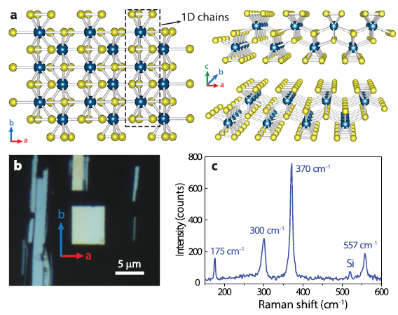
Figure 1. TiS3 as a quasi-1D layered semiconductor. (a) Crystal structure of TiS3, with unit cell lengths [43] a = 4.94, b = 3.39, c = 8.73 Å, layered in the c-direction with chains in the b-direction. Structures produced using VESTA [44]. (b) Optical reflection image of a TiS3 flake with a thickness of 32 nm on an amorphous quartz substrate exfoliated from bulk crystals. (c) Raman spectra of a flake displaying four specific TiS3 Raman peaks.
Download figure:
Standard image High-resolution imageAt lower energies, titanium trisulfide (TiS3) is one of the most interesting materials of the TMT family due to its direct bandgap around 1.1 eV [28] almost independent of thickness [29]. Its bandgap energy is close to that of silicon, adding promise for optoelectronics. Early work addressed part of the infrared optical signatures of TiS3, including reflection [20, 30] and absorption in the near infrared [18]. In recent years, after the successful fabrication of few-layer TiS3 ribbons and even monolayers [31], the optical properties of TiS3 have gained renewed interest [25, 28, 32–34]. At energies above the bandgap, there have been reports on photocurrent anisotropy [31], Raman spectroscopy [24, 35–38], and reflectance [32]. Recently, an exciton binding energy of 130 meV was experimentally measured in TiS3 ribbons using scanning tunneling spectroscopy and photo-electrochemical measurements [28]. An exciton lifetime of 140 ps was reported using time-resolved transient absorption measurements [39]. Both ab initio calculations and a variational approach have predicted the existence of excitons and their complexes in TiS3 monolayers [40, 41], awaiting experimental observation.
Here we report, for the first time, infrared light emission in ultrathin TiS3 microcrystals and evaluate its origin through polarization-, temperature-, and time-resolved photoluminescence spectroscopy. We find that TiS3 is a stable layered semiconductor with emission centered around 0.91 eV and a relatively high linear polarization anisotropy. Based on the power and temperature dependences of the photoluminescence, we attribute the emission dominantly to free excitons at room temperature and to bound excitons at low temperature.
Titanium trisulfide crystal structure
TiS3 consists of quasi-one-dimensional (quasi-1D) chains stacked in parallel sheets. In its crystal structure, titanium and sulfur atoms are arranged along chains in a special lattice direction [42] (b-axis in figure 1(a), with a chain identified by a black dashed line). The exfoliation plane is the ab plane. The bond lengths between titanium and sulfur atoms are shorter along the b-axis of the crystal.[31] As a result, the quasi-1D chain follows the b-axis indicating weaker Ti–S bonds along the a-axis. It leads to ribbon-shaped flakes for samples exfoliated from bulk TiS3 crystals [42] as directly observed in optical microscopy images (figures 1(b) and S1 (stacks.iop.org/TDM/7/015022/mmedia)).
We prepare TiS3 flakes by mechanical exfoliation from bulk crystals. All measurements except temperature-dependent PL are performed on the TiS3 micrometric flake on amorphous quartz in figure 1(b), with a thickness of 32 nm as determined by atomic force microscopy (figure S2(a)). Based on the orientation of the ribbons [45], we identify the a- and b-directions of the crystal with red and blue arrows, respectively. To compare the structure and composition of our TiS3 crystal with other works, we employ Raman microscopy to confirm the presence of the fingerprint phonon modes of TiS3. The Raman spectrum shows four prominent peaks at 175, 300, 370, and 557 cm−1 (figure 1(d)) corresponding to the Ag-type Raman modes, in good agreement with reports for bulk and few-layer TiS3 [46].
Infrared photoluminescence and anisotropy
First, we report infrared photoluminescence emission under excitation with a laser at 532 nm (figure 2(a)). It is, to the best of our knowledge, the first emission spectrum for this material. At room temperature, it is centered at ~0.91 eV (1360 nm) with a full-width at half-maximum (FWHM) of ~110 meV. We observe similar emission for other flakes with different thicknesses and on a different substrate (figure S1). We also measure the emission lifetime using time-resolved photoluminescence (figure 2(b)). The decay follows a single exponential function. A fit reveals a value of 210 ps for the emission lifetime, which is close to the 140 ps exciton lifetime reported for TiS3 ribbons using transient absorption [39]. The photostability of 2D semiconductors has a high impact on its potential for applications. Unlike bilayer black phosphorus [11], which is unstable in air and degrades under laser exposure, TiS3 shows excellent stability in ambient atmosphere (figures 2(c) and S4). It is photostable even under continuous laser exposure with a laser power that is two orders of magnitude higher than for black phosphorus.
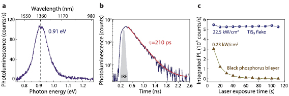
Figure 2. Infrared light emission from TiS3. (a) The photoluminescence spectrum of a TiS3 flake on a quartz substrate shows near-infrared emission centered at 0.91 eV (1360 nm). (b) Time-resolved photoluminescence of the TiS3 flake compared to the instrument response function (gray). The fit to a single exponential (red line) yields an emission decay time of 210 ps. (c) Photostability of a TiS3 flake compared to a black phosphorus bilayer using spectrally integrated photoluminescence versus continuous laser exposure time under ambient air conditions. The TiS3 flake shows excellent stability compared to black phosphorus.
Download figure:
Standard image High-resolution imageA significant consequence of the quasi-1D chain structure of TiS3 is its anisotropic optical properties, which we demonstrate through linear-polarization-resolved PL spectroscopy. In our polarization measurements, we independently control the linear polarization of the incident laser (excitation with electric field along either the a or b axes) and analyze the linear polarization of the emitted light (detection at intermediate angles between a and b). When excited with polarization along b, the emission exhibits a relatively strong emission anisotropy, as evidenced by PL spectra with detection along b and a (blue and red curves in figure 3(a)).
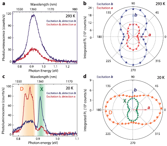
Figure 3. Linear polarization anisotropy of TiS3 photoluminescence. (a) Polarization-resolved emission spectra at room temperature (293 K), revealing in-plane linear polarization anisotropy in emission. The excitation laser at λ = 532 nm is linearly polarized along the b-direction of the crystal. On the detection path, an analyzer selects a- (red) or b-polarized (blue curve) components of the emitted light. (b) Integrated PL as a function of polarization detection angle for excitation laser polarized along the a- (red) and b-axes (blue spheres) for the same incident laser power. The data shows that there is anisotropy both in excitation and in emission. Solid blue and red lines are fitted curves using a cos2θ function plus an unpolarized contribution, where θ denotes the angle between the a-axis and the polarizer detection angle. (c) Polarization-resolved PL spectra at low temperature (20 K) with excitation along b and detection along b (blue) and a (red curve). The shaded areas split spectra into two regions with characteristic behaviors: D denoting defects and X denoting excitons. (d) Integrated PL as a function of θ for the spectral D (orange) and X regions (green spheres), solid lines are fitted curves as above. For all polarization measurements, the excitation power density is 25 kW/cm2.
Download figure:
Standard image High-resolution imageBy comparing the emission for excitation polarizations along b and a (figure 3(b)), we observe that the emission intensity along a (red) is always less than 25% of that along b (blue) regardless of the excitation polarization. This behavior is significantly different from ZrS3, where the PL is strongest along the excitation polarization direction [23]. Comparing figures 3(a) and (b), TiS3 has lower excitation polarization anisotropy in the visible (i.e. laser absorption) compared to its emission anisotropy in the infrared. To further understand the polarization anisotropy, we integrate the PL spectra over all wavelengths as a function of detection polarization angle θ (angle between the a-axis of crystal and the polarization analyzer axis). The results fit well to a cos2θ function plus a deviation from a perfect anisotropic emission due to unpolarized emission. Considering the large exciton binding energy of TiS3 (130 meV) [28], the observed independence of the emission anisotropy on excitation polarization points to an important role of excitons at room temperature [32].
At low temperature, the polarization dependence of the PL (figure 3(c)) is qualitatively different compared to room temperature. We can split the PL spectra at 20 K into two regions: the X region denoting excitons with the same behavior as room temperature emission; and the D region with a different behavior attributed to defects. To investigate this difference, we calculate the spectrally integrated PL intensity as a function of polarization detection angle θ in figure 3(d), which shows a clear 90° rotation between the X and D spectral regions. An estimation of anisotropy ratio from PL spectra (table S1) yields an increase in dichroic ratio value with decreasing temperature from 4 (at 293 K) to 5.3 (at 20 K) for the X region, confirming that the anisotropy in TiS3 depends on temperature.
Origin of the photoluminescence: temperature and power dependence
To elucidate the origin of the emission, we measure the PL as a function of excitation power density at both room and low temperatures (figures 4(a) and (b)). To fit the dependence on excitation power density with a power-law model, we introduce the slope c, defined as the ratio of the logarithm of the spectrally integrated PL and the logarithm of the excitation power density. At room temperature, the TiS3 emission exhibits super-linear dependence (c > 1). At low temperature, we consider independently the spectral regions D and X (orange and green in figure 4(b)). The X region follows a similar power law at room and low temperatures (c = 1.3 for X in figure 4(b)). Since the laser excitation energy is much larger than the band gap, a super-linear power dependence is expected for excitonic emission [47, 48]. On the other hand, the integrated PL of the peaks in the D region grows sub-linearly with pumping power (c = 0.7 for D in figure 4(b)), in agreement with the assignment to defects [48].

Figure 4. Origin of the emission in exciton and defect contributions. (a) Spectrally integrated PL intensity as a function of excitation power density measured at (a) room temperature (293 K) for the entire spectrum, and (b) low temperature (20 K) for the D (orange) and X (green) regions. The dashed lines are power-law fittings with super-linear behavior at room and low temperatures for the X region and sub-linear dependence for the D region.
Download figure:
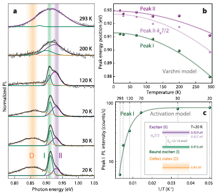
Standard image High-resolution imageTo gain further insight into the nature of the emission, we measure the temperature-dependent PL from another TiS3 flake on a thermally oxidized silicon substrate (Flake 5 in figures S1 and S2(b)). First, we focus our attention on the X spectral region. We distinguish two main contributions to the excitonic emission: I (green) and II (purple). By fitting the spectra with a set of Gaussian curves, a clear redshift of the energy of peaks I and II is apparent as the temperature increases (figure 5(b)). To investigate the relation between peaks I and II and as additional evidence for their excitonic nature, we follow their peak energy E(T) and fit their temperature dependence to the Varshni equation [49]
where T is the temperature, and A and B are phenomenological fitting parameters. From the fitting (supplementary table 2), we find 0.913 eV and 0.929 eV as peak energies at zero temperature for peak I and II, respectively. At first sight, the two peaks appear unrelated due to their different temperature dependence. However, if we subtract the thermal kinetic energy of free excitons (kBT/2) from all data points of peak II (light purple in figure 5(b)), the temperature dependence of both peaks follows a similar Varshni dependence. The loss of thermal energy suggests that the carriers are bound to defects. Considering both the thermal energy difference and the super-linear power dependence of peaks I and II separately (figure S5), peak I can be attributed to a bound exciton and peak II to a free exciton.
Figure 5. Temperature evolution of the photoluminescence. (a) PL spectra of a TiS3 flake at decreasing temperatures. The emission generally consists of two peaks of excitonic origin identified by I and II plus the defect contribution D. Solid lines are Gaussian fits. The excitation power density is 25 kW/cm2 with linear polarization along the b-direction of the crystal. (b) Energy of emission peaks I and II as a function of temperature. The dashed line shows a curve fit based on the Varshni equation. The light purple line represents peak II when thermal kinetic energy is subtracted. (c) Temperature dependence of the photoluminescence intensity of peak I (in log scale) versus inverse temperature, which follows an activation energy model with fitting results shown as a solid green line. Inset: Energy diagram of the peaks observed in temperature-dependent PL spectra.
Download figure:
Standard image High-resolution image
The PL intensity of peaks I and II also shows a distinct temperature dependence. At low temperatures, peak I dominates the excitonic emission (figure 5(a)). As the temperature increases, the intensity of peak I decreases, with peak II becoming dominant at higher temperatures. Excitons in TiS3 are expected to be stable due to the high exciton binding energy (130 meV) [28], consistent with the significant contribution of peak II at room temperature. The energy difference between peaks I and II is almost constant with temperature after removing thermal kinetic energy from free excitons to compare them with bound excitons (figure 5(b)). By analyzing the temperature dependence of the PL intensity (figure 5(c)), we find that peak I (green) starts to quench above 50 K. By fitting these results to an activation energy model (supplementary note 2 and supplementary table 3), we retrieve 12 meV as the activation energy of peak I, which is close to the difference between the energies of peaks I and II at low temperature (14 meV). Therefore, we assign such activation energy to the bound exciton binding energy, as summarized in the energy diagram in the inset of figure 5(c). Finally, we note that a possible alternative peak assignment would be that peak I is due to trions and peak D is due to defect-bound excitons. However, the difference in energies between peaks I and II at room temperature in our measurements under such an assignment would correspond to a trion binding energy of 30 meV, which seems excessive for multilayer films. Furthermore, trions usually follow the same Varshni dependence as excitons, which is not the case in our experimental data without subtracting thermal kinetic energy.
Conclusions
We have demonstrated infrared photoluminescence from exfoliated TiS3 crystals and investigated its dependence on polarization, time, power, and temperature. Our results show that TiS3 is a stable infrared 2D material with strong in-plane anisotropy originating from its unique 1D chain-like structure. We obtained 210 ps as emission lifetime. The temperature and power dependences suggest that the emission is dominated by free excitons at room temperature, while at low temperature bound excitons contribute the most to the emission. In the future, the fabrication of large area TiS3 films down to a monolayer and improvements in crystal quality could further increase its luminescence quantum yield, particularly when combined with strategies like chemical treatment [50]. TiS3 could thus provide an efficient and stable 2D semiconductor for emission and detection in the telecommunications O- and E-bands for integrated nanophotonic and optoelectronic devices.
Methods
Sample preparation
We deposited TiS3 flakes onto amorphous quartz substrates by mechanical exfoliation from bulk synthetic crystals (2D Semiconductors, Inc.) under ambient conditions. After optical measurements, the flake thickness was determined by atomic force microscopy by using a Bruker Dimension FastScan AFM system.
Raman spectroscopy
We used a confocal Raman microscopy system (Renishaw inVia) with a 514 nm excitation laser (power of 150 µW) and sample under ambient conditions.
Photoluminescence spectroscopy
Power-dependent, polarization-dependent, and temperature-dependent PL were collected using an optical microscope coupled to an Andor InGaAs iDus detector and spectrometer. A continuous-wave laser at 532 nm is used as excitation source. The excitation polarization was controlled with a Berek compensator (Newport) and the detection polarization analyzed with a wire-grid polarizer (Thorlabs). The laser was focused by a 50× NIR microscope objective (Mitutoyo) on the samples and the emitted light was collected with the same objective in an epifluorescence configuration using a long-pass dichroic mirror and a long-pass filter (Thorlabs DMLP605R and FELH0750). Temperature-dependent PL was carried out in an optical microscopy cryostat (Oxford Instruments Microstat HiRes II) with liquid helium. For lifetime measurements, we used a confocal micro-PL setup with time-correlated single-photon counting (TCSPC) electronics (Picoquant Picoharp 300). Laser pulses (λ = 760 nm, repetition rate 80 MHz, pulse width 70 ps), which trigger the start signal of the time-resolved measurement, are focused onto the sample by a 100× NIR objective (Mitutoyo). The PL emitted by the TiS3 flake is collected back by the same objective, and a dichroic mirror (cut-off wavelength 1000 nm) separates the PL from the reflection of the laser. The PL signal is then coupled to an optical fiber connected to a superconducting single-photon detector (Scontel SSPD).
Acknowledgments
We thank Raziman T V for useful discussions, J Gomez Rivas and A Fiore for access to the InGaAs camera and superconducting photon detector, and F van Otten for providing a photoluminescence alignment sample with quantum dots. This work was financially supported by the Netherlands Organisation for Scientific Research (NWO) through Gravitation Grant 'Research Centre for Integrated Nanophotonics' (024.002.033) and an NWO START-UP Grant (740.018.009).