
Abstract
Stanene has been theoretically predicted to be a 2D topological insulator with a large band gap, potentially hosting quantum spin Hall effect at room temperature. Here, few-layer stanene films have been epitaxially grown on Sb-terminated InSb (1 1 1) surface and their structural and electrical properties are characterized. Scanning tunneling spectrum results reveal a large bulk bandgap in single-layer stanene (over 0.2 eV). Moreover, spectroscopy evidence for a filled edge state near the steps was observed. The gap decreases dramatically with increasing number of layers, and multilayer stanene should become a Dirac semimetal in the bulk limit. The changeover may involve nontrivial topological phase transitions. Clear and reproducible Shubnikov–de Haas oscillations were observed on the single-layer stanene films that were exposed to atmospheric conditions for an extended period of time, showing the possibility for device experiments using nanofabrication and magneto-transport. Our results demonstrate that the single-layer stanene is a promising topological material for exploring fundamental physics and quantum applications.
Export citation and abstract BibTeX RIS

Original content from this work may be used under the terms of the Creative Commons Attribution 3.0 licence. Any further distribution of this work must maintain attribution to the author(s) and the title of the work, journal citation and DOI.
1. Introduction
Topological insulators (TIs) can host time-reversal symmetry protected surface state or edge state but with the gapped bulk band structures [1–3]. Quantum spin Hall effect (QSHE) has been theoretically proposed and experimental demonstrated in such two-dimensional (2D) TI systems [1–8]. It is of great values in both fundamental physics and material science owning to its promise for the realization of conducting channels without dissipation. However, for most of known 2D TIs, such as HgTe [1, 3], InAs/GaSb quantum wells [9, 10] and WTe2 films [8] et al, the band gaps are all relatively small, with the QSHE observed only at low temperatures. Novel TI materials with a large bandgap that can realize the QSHE at high temperature or even at room temperature are desirable. Monolayer  -tin film, also called stanene, has been demonstrated as a 2D TI with a sizable band gap of more than 0.3 eV [11–14]. In epitaxy, substrate plays a crucial role in shaping the properties of stanene [12, 15]. In previous experiments, stanene has been synthesized on various substrates [15–19]. Epitaxial growth of stanene on the InSb (1 1 1) surface with Sb- termination (B face) has been reported with a bandgap of about 0.44 eV [17, 20]. Furthermore, with increasing the thickness, the film transits from TI to Dirac semimetal [17], and, superconductivity has been detected in the few-layer stanene [15].
As we will report here, stanene with controllable layers has been epitaxially grown on the B face of InSb (1 1 1) and its atomic configuration and electronic properties have been investigated in situ under ultra-high-vacuum (UHV) by low energy electron diffraction (LEED), scanning tunneling microscopy and spectroscopy (STM/STS). Our results indicate Stranski–Krastanow (SK) growth mode takes place in epitaxial few-layer stanene on InSb (1 1 1) with post-growth-annealing. The initial Sn layer deposited on InSb acts as a wetting layer which has a strong hybridization with the substrate. We observed a large band gap on both the wetting layer (~0.35 eV) and the subsequently grown single-layer (~0.2 eV) stanene and the gap is found to reduce rapidly with increasing of the thickness. Spectroscopy evidences of edge states with energy inside the band gap, are observed on the steps of stanene film. And, with further increasing thickness, the stanene with multilayer behaves as a Dirac semimetal. More importantly, the single-layer stanene is found to be fundamentally stable when it is exposed to the ambient condition for an extended period of time, making it possible for carrying out nano-device fabrication process and low-temperature transport measurements. Here, Shubnikov–de Haas (SdH) oscillations have been observed in the single-layer stanene.
2. Experiment section
Our experiment was performed by utilizing a Unisoku-1300 STM/STS system equipped with a Sn thermal evaporation source and LEED. All STM/STS results are acquired in liquid helium temperature (4.2 K). Commercial InSb (1 1 1) wafers with chemical polished Sb- face were chosen as the epitaxial substrate. As schematically shown in figure 1(a), the lattice constants of InSb (1 1 1) and stanene are 4.58 Å and 4.62 Å, respectively. The stanene is buckled by Sn–Sn sp3 hybridization. If the bottom Sn atoms are well placed on the Sb atoms (figure 1(a)), there are chemical bonds between Sb and Sn atoms and the stanene lattices are compressed. It has been demonstrated varying substrate conditions considerably modulate the electronic properties of stanene, strain and an anion-terminated substrate are favorable for achieving a large gap in stanene film [12]. Prior to Sn atoms deposition, the substrates were cleaned by repeated cycles of Ar ion sputtering and subsequent annealing at 380 °C in the ultra-high vacuum chamber (~ Torr). The surface with atomic terraces and adatoms can be observed, as shown in figure 1(b). Atomic-resolution STM image in figure 1(c) reveals there is surface reconstruction which is frequently observed after the cleaning process of InSb (1 1 1) surface. The line profile along the blue line gives a lattice constant of slightly over 1.3 nm which is approximately 3 times as that of the native InSb (1 1 1) surface, which means the surface forms a 3
  3 reconstruction. It is confirmed by the LEED pattern collected at 30 eV on the processed surface of InSb (1 1 1), where the distance between the adjacent blue circled spots is 3 times larger than that of red circled spots. Increasing the electron energy to 55 eV, there appear six spots brighter than the others on the LEED pattern, revealing the 1
  1 configuration of the sublayer atoms. During epitaxial growth of few-layer stanene, 99.999% tin metal was used as the source. Sn atoms were evaporated at a rate of ~7 min per monolayer onto the InSb (1 1 1) surface at the substrate temperature of about 200 °C. Subsequently, the samples were further annealed at a temperature of 220 °C for 30 min. Stanene devices in Van der Pauw shapes were made with Ti/Au(10 nm/100 nm) contacts; the transport experiment under a magnetic field up to 9 T has been carried out in a 3He cryostat system (300 mK).
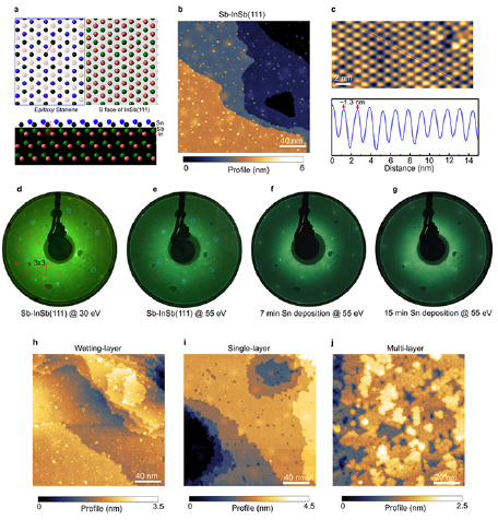
Figure 1. (a) Schematically shown the atoms alignment of epitaxial stanene on InSb (1 1 1) with Sb termination where the Sb atoms bond with the Sn atoms; (b) STM topographic image of InSb (1 1 1) surface after cleaning process in situ UHV chamber; (c) high-resolution STM image shows the reconstruction of surface atoms with a lattice constant of ~1.3 nm on InSb (1 1 1) after annealing; (d)–(g) LEED patterns collected on InSb (1 1 1) and Sn films with deposition for 7 min, 15 min and 22 min and annealed in UHV at 220 °C for 30 min. (h)–(j) Show the STM images of the wetting layer Sn film (7 min deposition), single-layer stanene (15 min deposition) and multi-layer stanene (22 min Sn deposition).
Download figure:
Standard image High-resolution image3. Results
It is an important question whether the reconstruction of InSb surface would influence the epitaxial growth of stanene. Figures 1(f) and (g) present the LEED patterns collected from samples with deposition of Sn atoms for 7 and 15 min, respectively. It reveals a 1  1 configuration similar to that of native InSb (1 1 1) substrate. We further increased the LEED electron energy to survey a larger momentum space, nevertheless we have not observed the diffraction of 3
  3 InSb reconstruction. This suggests the coverage of Sn film has recovered the InSb (1 1 1) substrate from 3
  3 reconstruction to the 1
  1 configuration owning to the bonding between Sb and Sn atoms. STM morphologies of the stanene with different thickness are presented in figures (h)–(j). It shows that, films with Sn atoms deposition for 7 or 15 min are continuous in morphology. On the other hand, for the sample with 22 min deposition of Sn atoms, islands can be easily observed. It suggests the
  -tin film epitaxial growth on InSb (1 1 1) as reported in this work shows a SK growth mode where the first layer acts as a wetting layer [21]. Layer by layer growth mode has been reported in epitaxially grown
  -Sn films on InSb (1 1 1) at room temperature [17, 20]. Here in our experiments, high-quality films with uniform lattice configuration are formed only after post-annealing at 220 °C, which enhances the hybridization between Sn and atoms of the substrate by forming Sn–Sb chemical bonds. Thus, the first layer of Sn is called the wetting layer and the second layer is the single-layer of stanene.
High-resolution topographic images in figures 2(a)–(c) provide a clearer description of SK growth mode. The wetting layer Sn on InSb (1 1 1) is atomically flat and nearly dislocation free. Triangle lattices can be distinguished in the atomically resolved tunneling image inset in figure 2(a), it matches the bulk configuration that the three top Sn atoms are more easily tunneled by STM. The tunneling signal is easily perturbed by the hybridization between Sn and Sb atoms in InSb substrate. The hybridization should help to enhance the large band gap in atom thick Sn film [12]. The line profile across the island above the wetting layer in figure 2(a) shows the thickness of the single-layer stanene is about 0.35 nm. A SK transition takes place with visible islands with defects (figure 2(b)). The formation of islands is energetically favorable to reduce strain in the film. Increasing the thickness, the density of the islands increases in the multilayer stanene (22 min Sn deposition) and the film is discontinuous as shown in figure 2(c). Figures 2(d)–(f) show the local differential conductance (dI/dV) spectra taken at the point far away from the edges (bulk) and near the step edges (edge) of the stanene films. There is a large band gap of about 0.35 eV in the bulk of the Sn wetting layer which is smaller than the angle-resolved photoemission spectroscopy (ARPES) data (0.44 eV) of monolayer stanene that grown on InSb (1 1 1) at room temperature without annealing, as reported in [17]. In contrast to the gap in the bulk, dI/dV at the edge shows a 'V-shape' spectrum with states filling in the bulk gap, which indicates the existence of a conductive edge state (figure 2(d)). Figure 2(g) presents dI/dV as a function of energy and distance away from the edge, it indicates the conductance is localized at the edge of the atom thick Sn wetting layer. The observed states could be the topological edge states as theoretically predicted [11], but the experimental results showing here are not sufficient to prove the topological nature of the states. Non-topological edge states, such as dangling bond states, could also exist. Figure 2(e) shows the conduction spectrum of single layer stanene film with a bandgap of about 0.2 eV, which may be induced by the release of strain and the reduced hybridization between Sb and Sn atoms. Meanwhile, a filled states located in the bulk gap can also be detected at the step edge. We further provide a STS map on single layer stanene at an energy of −100 meV as labeled by the dashed square in figure 2(b), and the results are shown in figure 2(h). A strong enhancement of state can be recognized along the step with perturbation by the defects. As mentioned before, STS in figure 2(f) no evidence for a clear gap, consistent with the notion that the multilayer stanene behaves as a Dirac semimetal [17].

Figure 2. (a)–(c) High-resolution STM images of the wetting Sn layer, and the single-layer and multilayer stanene; (d)–(f) Shows the STS of bulk and edge state; (g) dI/dV color scale map across the step edge shows the edge state on the wetting layer; (h) dI/dV conduction map collected at the sample bias of −100 mV shows the edge state along the step of single layer stanene.
Download figure:
Standard image High-resolution imageDirect observation of QSHE in transport measurements is a hallmark of a 2D TI. The stability of stanene film in ambient condition is critical for fabrication of devices and transport measurements. In figure 3(a), Raman scattering measurement has been performed on InSb substrate, the wetting layer Sn film (denoted as 1-Sn/InSb) and single-layer stanene (denoted as 2-Sn/InSb) that has been exposed in atmosphere for one week. A prominent peak ( ) originated from the in-plane vibrations of Sn atoms in stanene film can be observed in 2-Sn/InSb, demonstrating that the single-layer stanene is stable in the ambient condition [22]. However, we cannot observe the feature peak in 1-Sn/InSb sample, which provides a further proof that the first layer of deposited Sn film acts as a wetting layer. And its properties are easily modified by the absorption in the air.
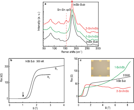
Figure 3. (a) Raman spectrum acquired from InSb (1 1 1) substrate (black), and as-grown wetting Sn layer (green) (denoted as 1-Sn/InSb) and the single layer stanene (red) (denoted as 2-Sn/InSb) exposed in ambient condition for one week; (b) The magneto-resistance of InSb substrate in both perpendicular magnetic field ( ) and parallel magnetic field
  B//) show field-induced metal–insulator transition at
  ; (c) The magneto-resistance of InSb substrate,1-Sn/InSb and 2-Sn/InSb at 300 mK in the perpendicular magnetic field. Inset shows the optical picture of the device.
Download figure:
Standard image High-resolution imageMagnetotransport measurements have been carried out on several Van der Pauw devices ( ) fabricated on InSb substrate, 1-Sn/InSb, 2-Sn/InSb samples. The optical image of the device is presented in the inset of figure 3(c). While our experiment does not directly address the topological properties of the material, the results provide information relevant to the bulk electronic structure. To obtain the intrinsic properties of stanene, it is crucial to eliminate the signal from bulk InSb substrate. Actually, at low temperature, n-typed InSb substrate goes through a magnetic-field-induced metal-insulator transition, under either a perpendicular or parallel magnetic field [23]. As shown in figure 3(b), when the magnetic field reach the phase-transition point (around
  here), the resistance of InSb dramatically increases and InSb quickly gets into the insulator phase. Generally, when the magnetic length
  becomes smaller than the mean distance between impurities, the electrons are localized in the vicinity of impurities, making the doped-InSb an electric insulator [24, 25].
As shown in figure 3(c), at  , for devices fabricated on InSb substrate, either 1-Sn/InSb or 2-Sn/InSb shows the longitudinal resistance
  with the same order of magnitude, indicating a large parallel conduction from the InSb substrate. However, at
  , the
, the  of the substrate dramatically increases owning to the magnetic-field-induced metal-insulator transition and the value is about 3500 times larger than the value of 2-Sn/InSb and 1-Sn/InSb samples at
  . It demonstrates that the Rxx and Rxy measured at
  shows the stanene properties rather than that of the substrate. Here, a strong oscillation has been observed in the
  of 2-Sn/InSb sample. The absence of oscillation in 1-Sn/InSb may be attributed to the strong hybridization between Sn and Sb, which strongly influences the energy band of the wetting layer.
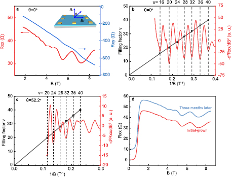
The longitudinal resistance  and Hall resistance
  of 2-Sn/InSb sample at
  are shown in figure 4(a). Periodic in 1/B of the
  oscillation indicates the SdH oscillation and the high quality of single layer stanene film. The negative slope of Hall resistance demonstrates the Fermi level lies in the conduction band. The filling factor index
  and the negative second derivate of
  versus
  are plotted in figure 4(b). Here, the factor 4 comes from the fourfold spin-valley degeneracy of the Landau levels in this case, similar to that of the bilayer graphene [26, 27]. Estimated from the period of SdH oscillations
  ) of the
  , the electron density is about
  . And the carrier mobility is found to be in the order of
  .
.
Figure 4. (a) The longitudinal resistance  (red) and Hall resistance
  (blue) of 2-Sn/InSb at perpendicular magnetic field
  . Filling factor index (black dot symbols) and second derivates of
  (red) versus 1/B are plotted in (b) with sample in perpendicular magnetic field and (c) in tilted magnetic field with
  . The minima of the
  oscillations are assigned for the integer filling factor. (d) The
  measured after device fabricated on initial-grown stanene film and device put in vacuum glovebox for three months (with 10 Ohm up shift).
Download figure:
Standard image High-resolution image
The magneto-resistance measurements are also performed in a tilted magnetic field. In figure 4(c), the period of SdH oscillation 
 ) is changed when the magnetic field with a tilted angle of
  . The ratio of the two periods
  obeys the relationship of
  . Notably, the SdH oscillation of 2-Sn/InSb sample barely changes even after the device is being stored in a low-vacuum glovebox for three months, as show in figure 4(d). The results demonstrate the single-layer stanene on InSb (1 1 1) is amenable to nanofabrication. Stanene device with gate modulation is a promising platform for future experiments on high temperature QSHE.
4. Conclusion
In this work, stanene with few-layer has been epitaxially grown on InSb (1 1 1) surface with the SK growth mode. The LEED patterns demonstrate the coverage of Sn films transits the 3  3 reconstruction of InSb (1 1 1) surface into the 1
  1 configuration, which results in each of the bottom Sn atoms located on the Sb atoms in the substrate. Localized dI/dV spectra reveals a large bandgap of more than 0.2 eV and the filled edge state near the steps in the single layer stanene. STS results confirms that, by increasing the thickness, the film transits from TI to Dirac semimetal. And the SdH oscillation has been observed in single layer stanene. Furthermore, single-layer stanene film is found to be stable under ambient condition. With further refined epitaxial techniques, stanene should enable a variety of experiments and devices based on high temperature QSHE.
Acknowledgments
The work at Peking University was funded by National Key R&D Program of China (No. 2017YFA0303301); Strategic Priority Research Program of Chinese Academy of Sciences (No. XDB28000000); NSFC for young scientist (NO.11704010); China's Post-doctoral Science Fund (NO. 2016M600844).