
Abstract
Sc has been employed as an electron contact to a number of two-dimensional (2D) materials (e.g. MoS2, black phosphorous) and has enabled, at times, the lowest electron contact resistance. However, the extremely reactive nature of Sc leads to stringent processing requirements and metastable device performance with no true understanding of how to achieve consistent, high-performance Sc contacts. In this work, WSe2 transistors with impressive subthreshold slope (109 mV dec−1) and ION/IOFF (106) are demonstrated without post-metallization processing by depositing Sc contacts in ultra-high vacuum (UHV) at room temperature (RT). The lowest electron Schottky barrier height (SBH) is achieved by mildly oxidizing the WSe2 in situ before metallization, which minimizes subsequent reactions between Sc and WSe2. Post metallization anneals in reducing environments (UHV, forming gas) degrade the ION/IOFF by ~103 and increase the subthreshold slope by a factor of 10. X-ray photoelectron spectroscopy indicates the anneals increase the electron SBH by 0.4–0.5 eV and correspondingly convert 100% of the deposited Sc contacts to intermetallic or scandium oxide. Raman spectroscopy and scanning transmission electron microscopy highlight the highly exothermic reactions between Sc and WSe2, which consume at least one layer RT and at least three layers after the 400 °C anneals. The observed layer consumption necessitates multiple sacrificial WSe2 layers during fabrication. Scanning tunneling microscopy/spectroscopy elucidate the enhanced local density of states below the WSe2 Fermi level around individual Sc atoms in the WSe2 lattice, which directly connects the scandium selenide intermetallic with the unexpectedly large electron SBH. The interface chemistry and structural properties are correlated with Sc–WSe2 transistor and diode performance. The recommended combination of processing conditions and steps is provided to facilitate consistent Sc contacts to WSe2.
Export citation and abstract BibTeX RIS
Introduction
Continuous engineering of contacts compatible with state-of-the-art semiconductor technology relies upon a detailed understanding of the critical relationships between processing conditions, interface chemistry and structure, and contact performance [1]. Silicides [2] and salicides [3, 4] exhibit a broad spectrum of composition-dependent contact resistances (Rc) and have long been employed as standard, low resistance contacts in traditional (Si, Ge) and compound (e.g. InGaAs) semiconductor-based CMOS technologies. Similar interface engineering has only recently been explored to improve Pd contacts to WSe2 [5], a semiconducting member of the transition metal dichalcogenide (TMD) family of two-dimensional (2D) materials, and is a promising, versatile strategy to engineer high-performance contacts comparable with Si technology (Rc ≈ 50 Ω cm) [6].
High defect concentrations (>1018 cm−3) [7–9], metal-TMD and metal-ambient gas reaction products [10–12], and spurious electrostatic effects [13, 14] often manifest as strong EF pinning [15] and/or large parasitic Rc, which can convolute the intrinsic properties (e.g. mobility) of a TMD-based device [16, 17]. A number of strategies have been employed to reduce Rc to TMDs, with varying degrees of success [18–24]. However, many are incompatible with typical back-end-of-line (BEOL) process flows, and direct metallization in top contacted devices is preferred. Impressive electron contact performance in MoS2 and black phosphorous (BP) devices has been demonstrated with Sc contacts [25–27]. However, Sc has yet to be explored as a contact metal in WSe2-based devices. Furthermore, the highly reactive nature of Sc lends to processing difficulties and metastable device performance [26, 27]. Sc spontaneously forms scandium oxide, a high-κ dielectric with a 5–6 eV band gap [28], even in ultra-high vacuum (UHV) conditions [10] and when a capping layer is employed to limit spurious air-exposure induced effects. Therefore, engineering high-performance Sc contacts to WSe2 requires a detailed understanding of the relationship between processing conditions, interface chemistry, and Sc contact performance.
WSe2 is also a promising alternative 2D switch in state-of-the-art magnetoresistive random-access memory technology due to the giant spin splitting in the valence band (456 meV) [29], moderate hole mobility [15], and low switching power. Spin-torque transfer based on the spin-valley Hall effect in WSe2 has emerged as a preferred magnetic bit-writing method in analogous devices [30] but relies on a single WSe2 layer, which can experience catastrophic damage during processing. Before the technology can be integrated in commercial applications, the effects of common BEOL processing conditions on the integrity of the WSe2 monolayer must be quantified.
In this work, we establish relationships between processing conditions (deposition chamber ambient, post-metallization annealing temperature and ambient), interface chemistry, and band alignment in the Sc–WSe2 system with in situ x-ray photoelectron spectroscopy (XPS) experiments. The number of WSe2 layers consumed by reactions with Sc after fabrication, 300 °C post-metallization anneals, and as a function of time between fabrication and characterization are quantified with Raman spectroscopy, scanning transmission electron microscopy (STEM), and energy dispersive x-ray spectroscopy (EDS). Scanning tunneling microscopy/spectroscopy (STM/STS) elucidate the effects of Sc atoms on the local density of WSe2 surface states, providing insight into the extracted band alignment. We demonstrate moderate EF depinning in metal-WSe2 systems by deliberate growth of a scandium oxide depinning layer at the contact-WSe2 interface. Finally, we evaluate the electrical performance of UHV-deposited Sc contacts to WSe2 field-effect transistors (FETs) as a function of post-metallization annealing conditions. Recommendations are provided to preserve the high-performance Sc electron contacts to WSe2 and to alleviate EF pinning in metal-WSe2 systems, which are based upon the impressive FET performance metrics and band alignment control demonstrated here.
Methods
Metallization, annealing, and in situ characterization
- (a)Depositing 1 nm Sc in UHV or high vacuum (HV): The synthetic WSe2 crystals employed in this work were purchased from HQ Graphene [31]. Before performing electron beam evaporation of Sc in UHV or HV, materials (WSe2, Sc metal) were prepared, the metal deposition rate was determined, and reference core level spectra were obtained identical to that employed and described in our previous work [10, 11]. Metal deposition was performed in UHV and HV using a similar base pressure of < 2 × 10⁻⁹ and deposition pressures of 7 × 10⁻⁹ mbar and 5 × 10⁻⁶ mbar, respectively. The Sc depositions in HV and UHV were performed in the same chamber. However, the deposition in HV was performed by first ramping the filament current up to the deposition current under UHV conditions, then backfilling the chamber with air to a pressure of 5 × 10⁻⁶ mbar, and subsequently opening the shutters to start the deposition. This method permits in situ XPS characterization after Sc deposition in HV unlike when the deposition is performed ex situ. A 50 nm thick Sc film was deposited on highly oriented pyrolytic graphite (HOPG) at RT in UHV and the reference Sc 2p core level spectrum was immediately obtained in situ.
- (b)Step-wise Deposition and Post-Metallization Annealing: All Sc depositions, anneals, and XPS characterization were performed in a cluster tool described elsewhere [32, 33]. Sc was deposited in UHV on separate bulk WSe2 crystals to estimated thicknesses of 0.1, 0.2, 1.0, 2.0, and 5.0 nm. Consecutive annealing steps were subsequently performed on each sample in UHV or forming gas (FG; 5% H2, 95% N2; 1 mbar) at 200 °C, 300 °C, and 400 °C for 1 h each. The stainless steel gas line connecting the FG cylinder to the annealing chamber was pumped overnight to a pressure of <2 × 10⁻⁹ mbar to remove any adsorbed species (i.e. H2O) from within the gas line before the chamber was backfilled with FG and the anneal was performed. XPS was performed after exfoliation and each subsequent deposition and annealing step to characterize the surface chemistry and the secondary electron cutoff. The secondary electron cutoff was measured to track the work function. The procedures employed to fit high-resolution core level spectra and construct band diagrams are discussed in detail in the supporting information (stacks.iop.org/TDM/6/045020/mmedia).
XPS instrumentation, parameters, and data analysis
XPS characterization was performed via a A monochromated Al Kα source and hemispherical analyzer (Omicron EA125) with ±0.05 eV resolution were employed for XPS. The cross sectional area of the incident x-ray beam is ~7.85 × 10⁻³ cm2. A 45° takeoff angle, 8° acceptance angle, and 15 eV pass energy were employed when acquiring high-resolution spectra. The analyzer was calibrated according to ASTM E1208 [34]. Spectra were deconvolved using the curve fitting software AAnalyzer [35].
Quantifying layer number consumption: sample fabrication and characterization
WSe2 flakes onto a SiO2/Si substrate (270 nm thermal SiO2). After transferring the samples into the cluster tool, the annealing chamber was pumped to a base pressure of < 2 × 10⁻⁸ mbar and then backfilled with Ar to 1 bar before annealing at 300 °C for 1 h to remove organic tape residue. Many 1 to 5 layer (1L to 5L) flakes were identified with optical microscopy, atomic force microscopy (AFM), and Raman spectroscopy. 5 nm thick Sc films were then deposited in UHV onto the WSe2 flakes (see supporting information for more details). Immediately after metallization, select samples were annealed in situ in UHV or FG at 300 °C for 1 h. A full coverage, 10 nm thick Si capping layer was subsequently deposited in situ using electron beam evaporation to protect the Sc–WSe2 heterostructure from spurious air-induced reactions during ex situ Raman spectroscopy. The anneals were performed before depositing the Si cap to prevent intermixing between Si and the underlying Sc–WSe2 heterostructure at elevated temperatures.
All Raman spectra were obtained using a laser power density of 0.49 mW µm−2 and a 0.2 cm−1 detector resolution. The Raman spectra were obtained from exfoliated WSe2 flakes after the vacuum anneal with 1 s exposure time and ten accumulations. After metallization and annealing (where applicable), Raman spectra were obtained using a 5 s exposure time and five accumulations. These parameters were carefully tuned to prevent laser-induced damage to WSe2 (see [5] for details regarding our carefully optimized Raman spectroscopy parameters).
Raman spectra were deconvolved with AAnalyzer to rigorously determine Raman shifts. A combination of Gaussian and Lorentzian functions was employed in the fitting process. The Lorentzian contribution varied with the number of WSe2 layers in the probed region and was therefore held constant for each set of spectra representing a certain number of WSe2 layers.
STEM and EDS
- (a)Lamella were milled from the Si/Sc/WSe2/SiO2 samples, which were initially fabricated for characterization by Raman spectroscopy, using a FIB electron microscope (FEI Nova 200 Dual Beam). High-resolution STEM was performed in an aberration corrected JEM-ARM200F instrument operated at 200 kV. Images were obtained using annular bright field and high angle annular dark field modes. EDS experiments were performed in an Aztec Energy Advanced Microanalysis System according to the procedure outlined in detail elsewhere [33]. EDS line scan data were acquired point by point (acquisition time ~0.5 s/pixel), which minimizes radiation damage in the lamella and increases the noise level in the data.
- (b)A lamella from a 65 nm Pd/5 nm Sc/WSe2 diode treated with atomic hydrogen (see below for details) was cross sectioned using an FEI Dual Beam Helios Nanolab 600i SEM/FIB microscope. Annular bright field TEM images were obtained with a JEOL 2100 operated at 200 kV.
Device fabrication
- (a)The backside gate dielectric was formed by depositing a 27 nm Al2O3 film onto a Si wafer (p++) at 250 °C and subsequently annealing the wafer at 400 °C in FG to reduce charge traps [36]. Al was then deposited by electron beam evaporation on the reverse side of the Si wafer as the backside contact. After exfoliating WSe2 flakes onto the Al2O3, source/drain contacts were defined using photolithography and Sc/Pd (20 nm/50 nm) contacts were subsequently deposited in UHV by electron beam evaporation. The sample was then transferred ex situ to an elastomer sealed electron beam deposition tool where 100 nm Au was deposited on top of the Sc/Pd layers. Finally, a lift-off process was performed. The devices were electrically characterized in air at RT and 1 bar in a Cascade Probe Station using a Keithley 4200 Semiconductor Characterization System.
- (b)Schottky Diodes: A bulk WSe2 crystal was exfoliated, resulting in a mirror-like (presumably low defect density) surface, and loaded into a UHV cluster tool [32, 33]. Select samples were treated with atomic hydrogen in situ prior to metallization. Sc/Pd contacts (65 nm Pd, see main text for Sc thickness details) were deposited through a shadow mask in UHV and 100 nm Au was subsequently deposited ex situ in an elastomer-sealed Temescal BJD-1800 electron beam evaporator [37] (base pressure < 5 × 10⁻⁶ mbar) to form arrays of circular contacts (diameters = 50, 100, 200 µm) across the WSe2 crystal. I–V curves were obtained by first sweeping from 0 to 2 V and then from 0 to −2 V (0.01 V step) to prevent hysteresis effects. Measurements were obtained after metallization and subsequent anneals in FG (1 mbar) at 200 °C, 300 °C, and 400 °C. I–V curves were obtained from all working diodes, normalized according to the area, and directly compared to confirm the electrical performance scales with area as expected.
Atomic hydrogen treatment
An MBE Komponenten Hydrogen Atom Beam Source (Model No. HCS-40-K-2000654) with tungsten filament was operated at a filament temperature of 1500 °C and a H2 (99.9999% purity) partial pressure of 5 × 10⁻⁶ mbar. The bulk WSe2 samples were maintained at a substrate temperature of 300 °C throughout the treatment, which was performed for 45 min. After the treatment and cooling to RT, the surface chemistry was characterized with XPS. Contacts were then deposited in situ.
Scanning tunneling microscopy and spectroscopy
A bulk WSe2 crystal was exfoliated and loaded into a UHV cluster tool described elsewhere [33]. The STM/STS images and spectra were acquired at RT in the constant current mode using an etched tungsten tip. Imaging under positive (negative) bias probes filled (empty) surface states within a few eV of the EF. The conductance (dI/dV versus V) curves obtained in this work are each differentiated averages of 20 curves obtained sequentially at a single location. STM images are processed in the WSxM software.
Results and discussion
Effects of processing conditions on the Sc–WSe2 interface chemistry and structure
Highly exothermic reactions between Sc, WSe2, and background gases in vacuum
The metal–semiconductor interface chemistry can vary significantly with the deposition chamber base pressure and the deposition rate [10–12, 38]. According to the kinetic theory of gases, the impingement rate of background gases on the substrate during deposition in HV is sufficiently high for continuous metal oxidation on the substrate surface. In addition, the reaction products formed between highly reactive metals, such as Sc, and TMDs also undergo exothermic reactions with the background ambient, complicating the interface chemistry further.
Sc aggressively reacts with WSe2 when deposited at RT regardless of the deposition chamber base pressure. Figure 1(a) shows the Se 3d and W 4f core level spectra obtained from exfoliated, bulk WSe2 after depositing ~1 nm Sc at RT in UHV or HV. When deposited in UHV, Sc completely reduces WSe2 to form metallic W and ScSex. The presence of metallic W is confirmed by the binding energy (BE) of the asymmetrically shaped, low BE chemical state in the corresponding W 4f core level spectrum (W 4f 7/2 BE = 31.30 eV), which is in close agreement with that of a metallic W reference (see Methods for details regarding the metallic W reference). The ScSex chemical state in the Se 3d core level spectrum is detected at lower BE from the WSe2 chemical state, which is expected considering, for example, the Pauling scale electronegativity of Sc (1.36) is much less than that of W (2.36) [39].
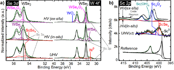
Figure 1. (a) Se 3d, W 4f , and (b) Sc 2p core level spectra obtained in situ after Sc deposition in UHV and HV on bulk WSe2 (base pressure <2 × 10⁻⁹ mbar in each case, see Methods for details on the deposition in HV). Significant reactions occur between Sc, WSe2, and background gases in the chamber, which completely convert Sc and ScSex to ScxOy when the deposition is performed in HV.
Download figure:
Standard image High-resolution imageOur previous work investigating the interface chemistry between transition metals and TMDs have shown that early transition metals typically oxidize in situ when deposited in HV [10–12]. However, the HV deposition was performed ex situ from the post metallization XPS in [10, 11]. In the aforementioned experimental design, it is difficult to explicitly determine whether the observed oxidation occurs in situ during metallization or while transferring the sample between the elastomer-sealed deposition tool and the UHV cluster tool. In this work, the HV Sc deposition was performed in the same chamber as the UHV deposition. However, the chamber was backfilled with air to 5 × 10⁻⁶ mbar before the deposition to simulate the conditions typically found in an elastomer sealed deposition tool. This experimental design eliminates any spurious air-exposure induced changes in interface chemistry and elucidates the true chemistry in the Sc–WSe2 system formed in HV. Sc was also deposited ex situ in an elastomer-sealed deposition chamber and subsequently characterized by XPS to compare the Sc–WSe2 interface chemistry formed in HV with and without air exposure between deposition and XPS.
Sc reduces WSe2 when deposited in HV with and without the air-exposure step between Sc deposition and XPS. When Sc deposition and subsequent XPS are performed in situ, the presence of substoichiometric WSex and ScSex are evidenced by the chemical states detected at 55.00 eV (31.73 eV) and 54.05 eV, respectively, in the Se 3d (W 4f ) core level spectrum. When the HV Sc deposition and subsequent XPS are performed ex situ, the WSex that presumably forms as Sc is deposited is oxidized, as evidenced by the appearance of WSexOy and WOx chemical states at higher BE from the bulk WSe2 chemical state in the W 4f core level (figure 1(a)). However, in a typical contact structure where a thicker Sc film and inert capping metal are employed, WSexOy and WOx are likely absent from the interface.
The additional grey peaks at low BE relative to the Se 3d and W 4f core levels correspond with the Sc 3s and Sc 3p core levels, respectively. The BE and area of these peaks were carefully calibrated according to a Sc reference film to maximize the accuracy of the fit (see supporting information for more details). When deposited in UHV, the majority of the ~1 nm Sc film reacts to form either ScSex or ScxOy (figure 1(b)). In contrast, all of the Sc deposited in HV is oxidized (including or excluding air-exposure between deposition and XPS). When Sc is deposited in situ in HV, a small concentration of ScSex is detected according to the low BE chemical state in the corresponding Sc 2p core level spectrum. This indicates that a small concentration of Sc reacts in situ with the underlying WSe2 when deposited in HV. Therefore, a Sc contact deposited in HV is mostly oxidized in situ, likely implicating contact performance considering Sc2O3 has been employed as a high-κ dielectric [40]. Nearly complete Sc oxidation in situ in HV is reasonable considering Sc–O bond formation is highly exothermic ( = −630 kJ mol−1) compared with the persistence of Sc–Se bonds (
 = −360 kJ mol−1) [41]. The presence of ScxOy and Sc(OH)x are corroborated by the chemical states detected in the corresponding O 1s core level (figure S3(b)).
Any reactions between adventitious carbon, which is detected on the exfoliated WSe2 surface at ~284.4 eV (figure S3(a)), or nitrogen in the background ambient are below the limit of detection. However, when a thicker Sc film is deposited on WSe2 in UHV, there is evidence for the formation of ScC and/or ScN, which is discussed in greater detail later.
Complete Sc oxidation at elevated temperatures in UHV
A complete understanding of the relationship between processing conditions, interface chemistry, and contact performance is critical to engineering the Sc–WSe2 interface for high-performance electron transport. Post-metallization annealing can drive additional reactions and concomitant EF shifts depending on the temperature and ambient. Therefore, the interface chemistry and band alignment between Sc and WSe2 were tracked in situ throughout stepwise Sc deposition in UHV and post metallization annealing (see Methods for experimental details).
Figure 2(a) displays the evolution of integrated intensities of chemical states associated with W0, ScSex, ScxOy , and metallic Sc formed after depositing ~5.9 nm Sc on WSe2 and subsequent UHV anneals. The integrated intensities displayed include both spin orbit split peaks in each of the Sc 2p , Se 3d, and W 4f core levels and are corrected by the appropriate atomic sensitivity factors unique to the detector employed (see supporting information). Sc reacts aggressively with WSe2 at RT to form metallic W and ScSex. A complete discussion regarding the evolution of chemical states in the Se 3d, W 4f , and Sc 2p core level spectra throughout Sc deposition at RT up to a total film thickness of 5.9 nm is included in the supporting information. The target Sc film thickness was 5 nm, but deviations from the calibrated deposition rate can manifest as a result of using Sc pellets as the source material instead of a solid Sc slug. In addition, calculating the Sc film thickness from core level attenuation requires the density of the attenuating film, which is difficult to estimate in this particular case considering the complex chemistry, which is discussed below.
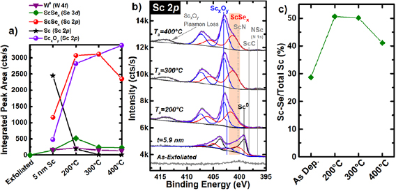
Figure 2. (a) Integrated intensities of chemical states in Se 3d, W 4f , and Sc 2p core level spectra associated with various reaction products as well as the (b) Sc 2p , core level spectra obtained from bulk WSe2 after exfoliation, depositing ~5.9 nm Sc in UHV, and subsequent in situ UHV anneals. (c) Percentage of the deposited Sc film converted to ScSex after RT deposition and subsequent UHV anneals, which depicts the aggressive reactions between Sc and WSe2 at RT and moderate intermetallic stability during 200 °C and 300 °C UHV anneals.
Download figure:
Standard image High-resolution imageThe 200 °C UHV anneal drives Sc to react with additional WSe2, which is evidenced by increases in the intensities of the ScSex (50.1% of the total Sc 2p core level intensity, figure 2(c)) and metallic W chemical states in the corresponding Se 3d and W 4f core level spectra (figures 2(a) and S4(a)). However, the concentration of ScSex decreases incrementally during the 300 °C and 400 °C UHV anneals, which indicates Sc–Se bonds are dissociated in favor of Sc–O bonds (as predicted by thermodynamics) [41]. In addition, the concentration of metallic W decreases slightly during the 300 °C and 400 °C UHV anneals, which suggests a reaction between metallic W and Se ions liberated from ScSex result in the reformation of W–Se bonds (figures 2(a) and S4(a)).
Figure 2(b) shows the Sc 2p core level spectrum obtained after depositing 5.9 nm Sc and after each subsequent UHV anneal. 28.7% of the 5.9 nm Sc film is converted to ScSex (Sc 2p : 400.27 eV) at RT (figures 2(b) and (c)), while the other 71.3% of the film is comprised of a mixture of metallic Sc (398.89 eV), ScxOy (402.16 eV), ScC (397.98 eV), and ScN (400.66 eV). ScC and ScN are near the limit of XPS detection, which is why they are difficult to resolve in figure 2(b). The presence of ScC and ScN in the same Sc–WSe2 system is validated in the discussion below.
During the 200 °C and 300 °C UHV anneals, all of the deposited metallic Sc either reacts with the underlying WSe2 to form ScSex and metallic W or with the outer ambient to form ScxOy as evidenced by the dramatic intensification of the ScSex and ScxOy chemical states in the corresponding Sc 2p core level spectrum (figure 2(b)). 17.9% of the ScSex formed during the 300 °C UHV anneal is converted to ScxOy during the 400 °C anneal (figure 2), which is thermodynamically favorable [41]. Extending the duration or increasing the temperature of the UHV anneal would presumably increase the relative ScxOy concentration within the film.
After depositing 3.2 nm Sc, a carbidic chemical state is detected at ~281.6 eV in the corresponding C 1s core level is detected at 281.60 eV (figure S5), which corroborates the presence of a small concentration of ScC. The formation of Sc–C bonds is exothermic at RT ( = −164 kJ mol−1) [42], which suggests ScC is present during initial deposition steps, but below the limit of XPS detection until a total of 3.2 nm Sc is deposited. The BE of the chemical state (~396.5 eV) detected after depositing > 3 nm Sc and throughout subsequent UHV anneals (figure 2(b)) is in good agreement with the ScN chemical state in the N 1s core level reported previously [43] and the ScN reference film grown in this work (figure S6). The evolution of chemical states in the C 1s core level throughout stepwise Sc deposition and subsequent UHV anneals as well as a detailed chemical analysis of the ScN reference film are discussed further in the supporting information.
Chemical states consistent with ScxOy and Sc(OH)x species are detected in the O 1s core level spectrum throughout the UHV anneals (figure S7) and are discussed in greater detail in the supporting information.
Intermetallic reduction via forming gas annealing
Annealing a TMD device in a partial pressure of H2 has been shown to passivate defects and improve performance [36, 44, 45]. Therefore, we investigated the effects of FG annealing on the Sc–WSe2 interface chemistry and band alignment. Prior to performing the FG anneals, stepwise Sc deposition at RT on bulk WSe2 results in the same Sc film thickness, interface chemistry, and EF position (figure S8) as were detected prior to the UHV anneals (figure 2).
The 200 °C FG anneal causes the metallic W chemical state in the corresponding W 4f core level to shift +0.30 eV and the ScSex chemical states in the Se 3d and Sc 2p core levels to shift −0.35 eV and +1.26 eV, respectively, relative to the chemical states detected after Sc deposition at RT. The aforementioned BE shifts indicate the formation of a ternary WxScy Sez compound (figures 3(b) and S8). The anneal also dissociates Sc–Se bonds, as evidenced by the small concentration of elemental Se detected at 55.30 eV in the corresponding Se 3d core level. Sc–Se bond scission is more favorable than W–Se bond scission considering the relevant bond dissociation energies (BDESc–Se = 385 kJ mol−1, BDEW–Se = 418 kJ mol−1) [46, 47]. After the 400 °C FG anneal, the WxScy Sez chemical states in the W 4f (Se 3d) core level shifts +0.42 eV (−0.34 eV) relative to that detected after the 200 °C FG anneal, which is consistent with a decreased concentration of Sc within the WxScy Sez compound and a corresponding increased oxidation state of the associated Wx+ component (figure S8). Thermodynamics indicates an additional anneal performed either for a longer period or at a higher temperature could completely dissociate Sc from WxScy Sez, potentially impacting contact resistance further. The gas line connecting the pressurized FG cylinder with the UHV annealing chamber was opened to the chamber overnight to remove adsorbed contaminants from the gas line before performing the FG anneals. However, the specific (presumably negligible) concentration of oxygen-based impurities within the FG and the associated effects on the scandium oxide concentration in the Sc film is not known in detail. Employing a molecular sieve in the gas line between the FG and the annealing chamber could cause additional variations in the chemistry and performance of the Sc contact to WSe2.
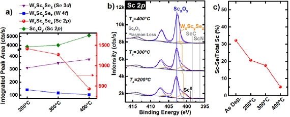
Figure 3. (a) Integrated intensities of the WxScy Sez intermetallic and ScxOy chemical states in the Se 3d, W 4f , and Sc 2p core level spectra. (b) Sc 2p core level spectra obtained from bulk WSe2 after Sc deposition at RT and subsequent in situ FG anneals. (c) Percentage of the deposited Sc film converted to ScSe intermetallic after deposition at RT and subsequent FG anneals showing aggressive reactions at RT and increasing Sc–Se dissociation with increasing FG anneal temperature.
Download figure:
Standard image High-resolution imageThe 200 °C FG anneal converts nearly all of the deposited Sc into either WxScy Sez or ScxOy (figure 3(b)). The intensity of the chemical state in the Sc 2p core level corresponding with the Sc–Se bond decreases by 64.1% during the 200 °C FG anneal. The Sc–Se contribution to the total intensity of the Sc 2p core level spectrum decreases to 18% and 5% after the 300 °C and 400 °C FG anneals, respectively (figures 3(b) and (c)), which contrasts the relatively stable intermetallic concentration throughout the UHV anneals. The ScN and ScC chemical states detected after the 200 °C FG anneal fall below the limit of XPS detection after the 400 °C FG anneal. This suggests the partial pressure of H2 in the FG ambient dissociates Sc–C and Sc–N bonds, which is an energetically favorable process (the energy liberated when a H–H bond is broken is greater than the BDEScC and BDEScN) [46].
This work indicates a Sc contact to WSe2 will completely oxidize when the post-metallization anneal is performed in FG, provided the anneal is performed at a high enough temperature or for a long enough time. Complete Sc–Se, Sc–C, and Sc–N bond dissociation in the presence of oxygen-containing species (i.e. the background gases in a vacuum chamber) are energetically favorable considering either the thermodynamics (see earlier sections for relevant  ) or the kinetics (BDESc–O > BDESc–N > BDESc–C > BDESc–Se > BDESc–Sc) [46] of the system. The effects of the increased ScxOy concentration on the band alignment and performance of the Sc contact to WSe2 will be discussed in detail later.
Multiple WSe2 layers consumed by thermally exacerbated reactions with Sc
The experiments discussed above were performed on bulk WSe2, which provides an appropriate platform to characterize effects of certain post metallization anneals on the metal-TMD interface chemistry and band alignment. However, FETs are typically fabricated with single and few layer TMDs. In addition, edge contacts exhibit superior performance compared to top contact analogs according to DFT calculations [48, 49] and experimental demonstrations [21, 49]. The true structure of the contact (edge versus top) will be affected by reactions at the metal-TMD interface. In addition, the broken inversion symmetry in WSe2 films with D3h symmetry is critical to the unique giant spin–orbit splitting in the valence band in the absence of an out-of-plane electric field [29]. It is therefore of interest to quantify the number of WSe2 layers affected by reactions with Sc.
Variations in structural and electronic properties of single and few layer TMDs due to interactions with a deposited metal have been investigated previously [50–52]. For example, depositing an incomplete coverage metal film on MoS2 resulted in a complex vibrational response due to metal-induced spatially varying strain across the TMD [51]. In this work, Raman spectroscopy is employed to quantify the number of layers consumed by reactions with Sc via a characteristic, layer number-dependent vibrational mode exhibited by WSe2. Special care was taken to ensure a full coverage Sc film was deposited (figure S2). In addition, a 10 nm thick Si capping layer was deposited in situ after the Sc deposition and the subsequent anneal (where applicable) to prevent any spurious, air-exposure induced changes in the Raman spectra obtained ex situ (procedure described in detail elsewhere) [5]. Therefore, any structural changes manifesting in the Raman spectra are attributed to Sc–WSe2 reactions. It is important to note here the Raman measurements were obtained within 24 h of Sc/Si deposition and the subsequent anneal.
The first (1st) order in-plane ( ) and out-of-plane (A1g) vibrational modes of WSe2 are degenerate and do not exhibit any discernible characteristic shifts or changes in intensity with layer number [53]. We recently demonstrated the layer number dependent Raman shifts exhibited by the second (2nd) order longitudinal acoustic mode at the M point in the Brillouin zone [2LA(M)] from single layer to five layer WSe2 [2.5 cm−1, 0.5 cm−1, 0.5 cm−1, and 0.3 cm−1 red shifts increasing from one layer (1L, 261.3 cm−1) to 2L, 2L to 3L, 3L to 4L, and 4L to 5L WSe2] [5]. Therefore, the number of WSe2 layers remaining after the Sc deposition and subsequent anneal can be accurately determined by tracking the Raman shift of the 2LA(M) mode. A λ = 532 nm laser is employed here to access the 2LA(M) mode via resonant excitation conditions [54]. The laser power density (0.49 mA µm−2), number of sweeps (5), and exposure time per sweep (5 s) employed in this work were carefully selected according to control experiments performed previously [5] to prevent laser-induced WSe2 damage. Therefore, spectral changes were confidently interpreted as indicators of chemical interactions between Sc and WSe2 rather than laser-induced intermixing.
Figures 4(a)–(c) display the Raman spectra obtained from exfoliated 1L, 2L, and 3L WSe2 flakes before and after depositing 5 nm Sc at RT and subsequent 300 °C UHV or FG anneals. Depositing 5 nm Sc at RT completely quenches the 1st and 2nd order modes of the 1L WSe2 flake, which indicates 1L WSe2 is consumed by reactions with Sc at RT (figure 4(a)). The 1.0 and 1.1 cm−1 red shifts and slight symmetric broadening exhibited by the 2LA(M) mode detected from the 2L and 3L WSe2 flakes, respectively, after depositing 5 nm Sc at RT suggest the interfacing reaction products cause stiffening (softening) of the A1g ( ) mode of the underlying WSe2 [51, 55].

Figure 4. Raman spectra displaying peaks corresponding with the  , A1g, and 2LA(M) vibrational modes of WSe2 obtained from 1L, 2L, 3L, and 5L (where applicable) flakes prior to and following (a) 5 nm Sc deposition under UHV conditions and subsequent post metallization anneal at 300 °C in (b) UHV or (c) forming gas. All spectra are normalized to the 2LA(M) peak unless vibrational modes are below the limit of detection. (d)–(f) Cross section STEM images and associated EDS spectra obtained from the same 3L WSe2 flakes investigated by Raman spectroscopy.
Download figure:
Standard image High-resolution imageAfter the 300 °C UHV anneal, the 1st and 2nd order vibrational modes of the 1L and 2L WSe2 flakes are completely quenched, while the 1st order modes exhibited by the 3L flake are near the limit of detection (figure 4(b)). This suggests at least two and possibly three WSe2 layers are consumed by reactions catalyzed during the 300 °C UHV anneal. To more explicitly quantify the number of layers consumed during the anneal, the vibrational modes of a 5L WSe2 flake were also probed throughout the experiment (figure 4(b)). After the anneal, the corresponding 2LA(M) mode exhibits a 1.2 cm−1 blue shift, which is consistent with a transition from 5L to 2L WSe2 [5]. The spectrum obtained from exfoliated 2L WSe2 (dotted line) is normalized to the 5L WSe2 spectra to clearly show the similarity between the spectrum of pristine 2L WSe2 and 5L WSe2 after Sc deposition and subsequent 300 °C UHV anneal. Therefore, we confidently conclude that three WSe2 layers are consumed by reactions with Sc during the 300 °C UHV anneal.
Interestingly, 1L WSe2 exhibits 1st and 2nd order modes above the limit of detection after the 300 °C FG anneal despite significant reactions detected by XPS in this work. In addition, asymmetric broadening towards lower wavenumber is detected in the 1st order modes of all WSe2 flakes after the FG anneal. This behavior indicates Sex+ (liberated by Sc–Se bond scission) reacts with metallic W to form defective WSex clusters, which is consistent with the Raman spectrum obtained from a WSe2 film lacking long range order [55] and also the XPS results displayed in figure 3.
Roughly nine months after characterizing the three different 10 nm Si/5 nm Sc/3L WSe2/270 nm SiO2/Si samples with Raman spectroscopy (figures 4(a)–(c)), lamella were milled and imaged by STEM. The corresponding STEM images are shown in figures 4(d)–(f). After Sc deposition at RT (figure 4(d)), nanocrystalline grains with lattice spacing of 0.21 nm are observed in the Sc film, which is consistent with the Sc{111} family of planes [56]. A significant concentration of oxygen is detected by EDS throughout the Sc film (figure S9). However, the lattice spacing of the grains observed in figure 4(d) is not consistent with that of Sc2O3 (0.31 nm) [57], which indicates the oxygen is dispersed in amorphous regions of the film between grains. Se and W diffusion into the Sc film is observed in the corresponding EDS (figure 4(d)). The three ~0.7 nm thick stripes of dark contrast coincide with high-Z W atoms and therefore indicate the presence of three WSe2 layers (figure 4(d)). The top most WSe2 layer in figure 4(d) appears to have retained its planar structure in some regions, but the contrast is slightly different from the underlying two layers indicating some disruption of the top layer due to intermixing in general agreement with the corresponding Raman spectra in figure 4(a).
When a lamella is milled from an analogous Sc–WSe2 sample fabricated at RT in UHV (see supporting information for details) within two weeks of fabrication and imaged immediately, a 2.0–2.5 nm thick amorphous region is observed between Sc and WSe2 in the corresponding TEM images (figure S10). Therefore, the WSe2 involved in reactions with Sc undergoes restructuring over time as Sc oxidizes, leading to the physical differences observed by TEM in this work depending on the time between fabrication and imaging.
The thickness of the dark contrast region observed after the 300 °C UHV anneal (~2.0 nm, figure 4(e)) is consistent with that expected of pristine 3L WSe2. However, individual layers are no longer distinguishable, which suggests significant intermixing occurs between WSe2 and Sc and corroborates three WSe2 layers are consumed by reactions during the 300 °C UHV anneal. An amorphous region is observed between the disordered WSe2 and the polycrystalline Sc film, which likely corresponds with the ScSex intermetallic detected by XPS after the same anneal. EDS indicates Se and W diffuse ~3 nm up into the Sc film and down into the SiO2 substrate. The 0.30 nm lattice spacing exhibited by the nanocrystallites in the Sc film after the anneal (figure 4(e)) indicates the dramatic increase in scandium oxide detected by XPS after the same anneal (figure 2) corresponds with the formation of a polycrystalline Sc2O3 film.
After the 300 °C FG anneal, local atomic structure and interlayer van der Waals gaps are resolvable in the corresponding STEM image (figure 4(f)). EDS indicates Se and W diffuse 2–3 nm into the Sc film, while Sc, Se, and W diffuse up to 5 nm into the underlying SiO2 (dark regions below the WSe2). Metal diffusion into the underlying dielectric in back-gated devices could impact the device performance (e.g. decreased gate modulation, increased off current). The WSe2 film is comprised of disordered regions with limited atomic order adjacent regions of 3L WSe2 with clearly resolvable van der Waals gaps between each layer. These observations corroborate our hypothesis, based on the corresponding XPS (figure 3) and Raman results; W–Se bonds re-form via Sc–Se bond dissociation throughout the FG anneals.
In a device where the contact metal consumes at least one TMD layer, the resulting intermetallic likely remains in intimate lateral contact with the adjacent channel. Therefore, any TMD layers in the contact region consumed by reactions at the metal-TMD interface should be considered pseudo-edge contacts, which may exhibit superior performance to the top contact analog. In addition, understanding changes in the band structure of few layer TMDs associated with interface reaction-induced layer number thinning is critical to engineering superior performance in a wide variety of TMD devices. For instance, maintaining an odd number of layers in the channel of a WSe2 spin valve is critical to device operation.
Band alignment and electrical performance of the Sc contact to WSe2
The EF shifts towards the conduction (valence) band edge will be referred to in the following discussion as positive (negative). Figure 5(a) displays the absolute BEs of the WSe2 chemical state in the Se 3d5/2 core level spectra detected from WSe2 after exfoliation and subsequent stepwise Sc deposition and post-metallization annealing6.
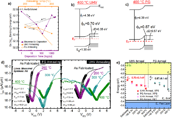
Figure 5. (a) Binding energies of the bulk WSe2 chemical state in the Se 3d core level spectra throughout stepwise Sc deposition and post-metallization annealing in either UHV ♦ or FG ◊ conditions. The BE shifts throughout RT Sc deposition are similar for both samples, which is why the data points obtained from the 'FG anneal' sample prior to the anneals are displayed in (a). Band alignments after the samples are annealed in (b) UHV and (c) FG at 400 °C, which are derived from XPS measurements. The error of ± 0.1 eV is associated with all Fermi level positions depicted. (d) IDS–VBG characteristics (solid lines) measured from back gated few layer WSe2 FETs with Sc contacts after fabrication and subsequent annealing in UHV or FG. The symbols in (d) correspond with fits of the IDS–VBG obtained with an analytical Schottky barrier model to extract the electron and hole Schottky barrier heights (SBH) throughout the anneals. (e) Band alignment between Sc and WSe2 after contact deposition and post-metallization anneals according to XPS in (a) and the analytical fits of the IDS–VBG curves in (d). Band diagrams in (b) and (c) are reflected in (e). The ambipolar FET characteristics obtained after FG and UHV anneals corroborate the mid-gap band alignment indicated by XPS.
Download figure:
Standard image High-resolution imageAfter exfoliation, the EF is detected 0.95 ± 0.15 eV from the WSe2 valence band edge according to the initial valence band offset and secondary electron cutoff (0.95 ± 0.07 eV, 4.36 ± 0.08 eV, respectively; figure S11). The bulk WSe2 chemical states initially shift to lower BE during the first two Sc depositions. In contrast, the EF shifts towards higher BE beyond an effective Sc film thickness of 5 Å. The WSex and ScSex formed during initial Sc depositions likely shift the EF towards the valence band, while the metallic Sc that accumulates in latter depositions shift the EF towards the conduction band. Depositing 5.7 nm Sc at RT in UHV shifts the WSe2 chemical states −0.09 eV (figure 5(a)) from the BEs detected after exfoliation, which corresponds with the formation of a 0.44 ± 0.15 eV electron Schottky barrier. The appreciable Schottky barrier detected here is far from the expected Ohmic electron band alignment expected between Sc and WSe2 considering the low metal work function (3.5 eV) [58]. It is possible the metallic W, formed as a product of the Sc–WSe2 reaction, dominates the band alignment in an unannealed Sc contact to WSe2 (polycrystalline tungsten work function ≈4.5 eV) [58].
As the UHV anneal temperature increases, the EF shift towards lower BE increases in magnitude, exhibiting a total −0.26 eV shift after the 400 °C UHV anneal. The EF shift corresponds with an increased electron SBH to 0.70 ± 0.15 eV (figure 5(b)).
The band alignment between Sc and a separate bulk WSe2 crystal after exfoliation, Sc deposition, and subsequent FG anneals (figures 5(a) and (c)) is similar with that detected in the 'UHV anneal' sample. A more detailed discussion of the band alignment between Sc and bulk WSe2 throughout annealing in FG is provided in the supporting information.
EF pinning occurs due to gap states in the semiconductor that can be generated by defects, interface reactions, or a deliberately placed re-pinning layer [59]. An appreciable concentration of oxygen deficient ScxOy in the Sc film could generate gap states in the underlying WSe2, producing the near-midgap alignment detected after the 400 °C anneals. When annealing is performed in UHV, the chemistry, and therefore the electrostatics of the junction, are also convoluted by ScSex. The Ohmic hole band alignment reported recently between Pd and WSe2 after a 400 °C FG anneal was facilitated by passivating defects at the interface with atomic hydrogen in the FG ambient [5]. However, the beneficial effects of hydrogen-induced defect passivation on the Sc contact to WSe2 are either negligible compared with the interface chemistry effects or require hydrogen radicals, which are not readily catalyzed from H2 by Sc as they are in Pd.
To corroborate the XPS-derived near-midgap band alignment with the electrical performance of Sc contacts to WSe2, back-gated, few-layer WSe2 FETs were fabricated on an Al2O3/Si substrate with 20 nm Sc/50 nm Pd/100 nm Au contacts. It is difficult to accurately extract SBHs from ultra-thin body transistors in which the depletion width is defined by the thickness of the region under the contacts, such as in few-layer TMD FETs. Therefore, an analytical Schottky barrier model based on Landauer transport theory [14] was employed here to extract electron and hole SBHs from the measured IDS–VBG characteristics of our few layer WSe2 FETs with Sc contacts. The model, which has been employed in recent works [14, 15, 26, 27], accounts for thermionic emission and the appreciable tunneling contribution to the total current due to the ultra-thin body of the devices. After fabrication, the Sc–WSe2 FETs exhibit impressive ION/IOFF ratios in the order of 106, subthreshold slope (SS) of 109 mV dec−1 (among the best reported to date) [16], and electron SBHs of 0.4–0.45 eV (figure 5(d)), which are in good agreement with the corresponding XPS-derived 0.36–0.44 eV electron SBH (figure 5(e)). Analogous WSe2 FETs with Pd contacts exhibit a larger 0.73 eV electron SBH, which is likely attributed to photoresist residue-induced EF pinning [5, 24]. Sc mitigates EF pinning effects induced by photoresist residue in as-fabricated devices by reacting with the WSe2 at RT and 'cleaning' resist residue from the interface. Reactions between Sc and common resist polymers are favorable considering Sc–C, Sc–N, and Sc–O bonds are all detected in a resist-free Sc–WSe2 system, as discussed earlier.
The 400 °C UHV and FG anneals convert 59.9% and 94.9% of the Sc film to ScxOy , respectively. According to the analytical Schottky barrier model, the UHV and FG anneals increase the electron SBH to 0.70 eV and 0.87 eV, respectively (figures 5(d) and (e)). The additional 0.17 eV EF shift towards the valence band detected after the FG anneals could be related to the much higher ScxOy concentration within the deposited film, considering the charge neutrality level of Sc2O3 (~5.3 eV) [28, 40] aligns closely with the WSe2 valence band edge. In addition, the ION/IOFF ratio decreases by ~103 and the SS increases by approximately a factor of 10 after the UHV and FG anneals. High performance Sc electron contacts to BP have recently been demonstrated [26, 27]. One study correlates significant improvements in n-type device performance with the formation of a ScxOy layer between the Sc contact and BP over one month in ambient conditions [27]. ScxOy formed in the presence of hydroxide molecules (e.g. gettered from air), such as the ScxOy that formed over time at the Sc–BP interface, contains a significant concentration of hydrogen (figure S7), which presumably affects the conductivity. The anneals performed in this work dehydrogenate the ScxOy in the Sc films on WSe2 [28] resulting in the degraded performance measured with increasing anneal temperature. Therefore, post-metallization anneals in a reducing environment (e.g. UHV or FG) should be avoided to prevent device performance degradation, maximize the gate modulation, minimize the turn-on voltage, and maintain a low electron SBH when Sc contacts are employed.
Controlling the contact polarity by inserting a ScxOy interlayer
EF depinning at the contacts in devices based on 2D materials has been achieved by inserting a tunnel barrier [15, 60] or 're-pinning' layer [59] between the contact and the channel. ScxOy has only recently been explored, albeit unintentionally, as an interlayer to control contact performance [27]. In this work, WSe2 was treated with atomic hydrogen to etch the surface, which promotes surface oxidation in situ in UHV (figure S12, see supporting information for details). Pd/Sc contacts were then deposited in situ, in UHV, at RT, and through a shadow mask to reactively form a ScxOy interlayer between the metal and the WSe2. Sc scavenges oxygen from WOx during the UHV deposition, forming an interfacial ScxOy layer. A 3 nm Sc film was deposited on one sample to form an interlayer entirely comprised of intermetallics and ScxOy and therefore facilitate hole dominant conduction via the Pd layer. 15 nm Sc was deposited on another atomic hydrogen-treated sample to form a substantial metallic Sc layer between the ScxOy interlayer and the Pd capping layer, which facilitates electron dominant conduction.
The forward bias currents measured from the 65 nm Pd/5 nm Sc/WSe2 diodes were transformed according to equation (1) [62]

where I, q, V, k, and T represent the measured current, electron charge, applied bias, Boltzmann's constant, and temperature, and the linear region in each curve between 0.15 V and 0.35 V was fitted using linear regression. The Richardson constant (33.9 A cm−2 K−2,  = 0.33) [63], SBH (0.85 eV), and an ideality factor (1.00, averaged from 5 diodes) are calculated from the slope and intercept of the best fit line to the I–V curve obtained at 110 °C (figures S13(a) and (b), see supporting information for details) [62]. An ideality factor of 1.00 indicates the barrier height is homogeneous across the interface. This suggests the atomic hydrogen treatment coupled with the ScxOy interlayer eliminate defects at the interface unlike the highly inhomogeneous barrier formed at the inert Pd–WSe2 interface at RT. However, the EF resides much closer to midgap when the ScxOy interlayer is included between Pd and WSe2 compared with the Ohmic hole band alignment exhibited by Pd contacts to WSe2 at RT [5]. Some metallic Sc is likely present within the interlayer and contributes to the near-midgap alignment measured here.
The transformed, annealing-temperature-dependent I–V curves obtained from the 65 nm Pd/15 nm Sc/WSe2 Schottky diodes yield ideality factors >3 in all cases, which indicates the corresponding SBH will be unreliable. However, an Arrhenius plot of the reverse bias I–V characteristics of the 65 nm Pd/15 nm Sc/WSe2 Schottky diodes yields a linear pattern, from which a 0.34 eV electron SBH is extracted. The 0.34 eV electron SBH obtained with the 15 nm Sc layer deposited onto the atomic hydrogen-treated WSe2 is 0.51 eV smaller than the diodes where only 3 nm Sc was deposited (figures 6 and S13(c)) and ~0.1 eV less than Sc–WSe2 FETs after metallization at RT. The contact structures, fabrication and processing details, and SBHs of all devices from this work are summarized in table 1. Therefore, electron dominant conduction is facilitated by the low work function metallic Sc layer that accumulates on top of the interfacial ScxOy . More effective EF depinning may be achievable with scandium oxide by tuning the ScxOy layer to minimize the thickness and maximize the tunneling current or by directly depositing the ScxOy rather than depositing metallic Sc on oxidized WSe2.
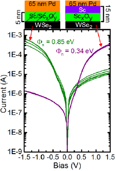
Figure 6. I–V characteristics obtained from Pd–Sc–WSe2 Schottky diodes deliberately treated with atomic hydrogen before metallization to form an interfacial ScxOy interlayer.
Download figure:
Standard image High-resolution imageTable 1. Schottky diode and FET contact structure, fabrication details, and electron SBH after processing.
| Sc Thickness | Pd Thickess | Anneal Temperature | Anneal Ambient | Atomic Hydrogen Treatment | Electron SBH |
|---|---|---|---|---|---|
| 20 nm | 50 nm | N/A | N/A | N/A | 0.44 eV |
| 20 nm | 50 nm | 400 °C | UHV | N/A | 0.70 eV |
| 20 nm | 50 nm | 400 °C | 95% N2, 5% H2 | N/A | 0.87 eV |
| 3 nm | 65 nm | N/A | N/A | 45 min | 0.85 eV |
| 15 nm | 65 nm | N/A | N/A | 45 min | 0.34 eV |
The electron Schottky barrier formed between Sc and WSe2 can be reduced by limiting the intermetallic concentration (i.e. minimizing intermetallic-induced gap states). The contact structure, fabrication and processing details, and employing an optimized, oxygen deficient ScxOy interlayer will minimize reactions with WSe2 and also provide greater EF control when other contact metals are employed in conjuction with the interlayer.
Local density of states around Sc atoms/clusters on WSe2: STM and STS
The Sc–WSe2 diodes and FETs discussed above exhibit appreciable 0.4–0.45 eV electron SBHs at RT, which is unexpected considering the work function of Sc (~3.5 eV) is smaller than the electron affinity of WSe2 (~4.1 eV) [9, 61]. Scanning tunneling microscopy (STM) and spectroscopy (STS) elucidate the surface topography and local density of states (LDOS). Therefore, STM and STS can provide insight into changes in the electronic structure of the WSe2 surface induced by Sc in the earliest stages of metallization (i.e. after depositing a <3 Å Sc film). The exfoliated WSe2 surface before metallization is atomically flat with a random distribution of atomic scale defects across the surface, similar to previously published STM images from bulk WSe2 [9]. The upper and lower STM images in figure 7(a) were obtained in situ under positive and negative tip bias, respectively, from exfoliated, bulk WSe2 after depositing ~1 Å Sc in UHV at RT. Sc atoms/clusters appear as small bright spots surrounded by large dark regions under forward bias, while they appear as large bright patches and ~2 nm diameter rings under reverse bias. The dark contrast exhibited by Sc regions in positive bias indicate an associated high resistance tunneling barrier and therefore fewer occupied LDOS. Sc oxidation occurs in UHV and therefore could contribute to the suppressed LDOS around Sc when 'filled' states are probed.

Figure 7. (a) STM images obtained from WSe2 after a ~1 Å Sc film was deposited in UHV with the upper (lower) image obtained at 1.5 V and 0.5 A (−1.8 V and 0.8 A). (b) STS conductance spectra obtained from points spanning a ~3 nm diameter Sc cluster and the surrounding WSe2 showing the significant increase in density of states below the WSe2 EF when the tip probes directly over the Sc cluster. Each spectrum is a differentiated average of 20 sweeps over the same spot. The spectra are manually offset to more clearly show the features in each spectrum. (c) High resolution STM images obtained from the same 1 Å Sc–WSe2 sample showing atomic resolution in a region of bare WSe2, rings of bright contrast reflecting charge redistribution around single Sc atoms (some indicated by green arrows), and larger Sc clusters.
Download figure:
Standard image High-resolution image
Five STS spectra were obtained in an array spanning a Sc cluster and the surrounding WSe2 (dots in figure 7(a), lower image). The bare WSe2 exhibits a band gap of 1.32 ± 0.05 eV, which is consistent with previous STM studies of bulk WSe2 (figure 7(b)) [9]. The EF is detected 0.33 ± 0.05 eV from the valence band edge, which is consistent with the XPS-derived band alignment of exfoliated WSe2 in this work. As the tip approaches the Sc cluster, the reverse bias conductance and density of gap states below the EF increase and reach a maximum when the tip is positioned directly over it. The enhanced density of states in the valence band observed over Sc clusters is qualitatively consistent with the EF shift away from the conduction band detected by XPS after depositing Sc on WSe2.
In high resolution reverse bias images (figure 7(c)), individual Sc atoms and the associated Sc–Se bonds are inferred from numerous ~2 nm diameter rings of bright contrast (pointed out by arrows). These regions exhibit central symmetry, which suggests a 1D feature (i.e. a single atom) is present at the center. Similar features were observed via STM around isolated Mo atoms at interstitial sites in the MoTe2 lattice [61]. The ring of bright contrast observed in reverse bias images manifests as a result of charge transfer from Sc to the surrounding Se atoms, similar to the charge redistribution associated with mirror twin boundaries in TMDs. Therefore, the formation of Sc–Se bonds and the associated enhanced density of states below the WSe2 EF contribute significantly to the unexpectedly high electron Schottky barrier formed between the Sc contact and WSe2.
Discussion
The physical characterization, EF shifts according to XPS, and electrical characteristics of Schottky diodes and FETs indicate the WSe2 FETs exhibit the lowest electron SBH, the highest ION/IOFF ratio (~106), and the steepest SS (109 mV dec−1) when the intermetallic concentration at the Sc–WSe2 interface is minimized and the concentration of metallic Sc within the contact is maximized. In this work, the lowest electron SBH between Sc and WSe2 (0.34 eV) is achieved by oxidizing the WSe2 surface prior to Sc deposition, which both limits the Sc–WSe2 reaction and avoids the deleterious post-metallization anneals. Inserting an inert, oxygen-free tunneling layer (e.g. hBN) [15] between Sc and WSe2 would more effectively prevent the Sc–WSe2 reactions and decrease oxygen concentration in the Sc layer compared to the reactively formed ScxOy interlayer employed in this work, likely resulting in the highest performance Sc contact to WSe2. Sc immediately consumes one WSe2 layer at RT and at least three layers during the post-metallization anneals. This work establishes relationships between the Sc–WSe2 interface chemistry, structure, and band alignment associated with specific pre- and post-metallization processing steps, which are integral to engineering consistent, high-performance Sc contacts to any TMD. Critically, we demonstrate high performance n-type WSe2 FETs with Sc contacts and establish processing conditions (both to employ and to avoid) for consistent, high-performance n-type Sc contacts.
Conclusions
This work demonstrates high-performance n-type WSe2 FETs with impressive ION/IOFF (106) and SS (109 mV dec−1), which is achieved without any post-metallization processing and by depositing the Sc contacts in UHV. Mildly oxidizing the WSe2 surface at the contact regions before metallization reduces the electron SBH formed between Sc and WSe2 at RT by 0.10 eV as a direct result of the minimized concentration of scandium selenide at the interface. The largest electron SBHs of 0.70 eV and 0.87 eV (400 °C UHV and FG, respectively) worst SS (~1 V dec−1), and lowest ION/IOFF ratios (~103) are measured when post-metallization anneals are employed, which contrasts the highest performance Pd contacts to WSe2 after the same anneal. XPS indicates the anneals increase the electron SBH by 0.4–0.5 eV and completely oxidize the Sc contact, which cause the aforementioned degraded device performance. STM and STS explicitly relate the unexpectedly large electron SBH observed between Sc and WSe2 throughout this work with an enhanced LDOS below the WSe2 EF in the presence of Sc–Se bonds, which necessitates processing steps that minimize the Sc–WSe2 reaction. The significant reactions between Sc and WSe2 are corroborated by Raman spectroscopy and STEM, which indicate 1L WSe2 is consumed at RT and at least three WSe2 layers are consumed during the anneals. The processing condition-dependent number of WSe2 layers consumed by Sc is a critical benchmark for future device architectures based on WSe2, especially those relying on the giant spin-Hall effect that occurs in WSe2 with D3h symmetry. This work shows a detailed understanding of the relationships between processing conditions, interface chemistry, and contact performance can be leveraged in any metal–TMD system to consistently achieve the highest device performance.
Acknowledgment
The authors would like to thank A Yu (Massachusetts Institute of Technology) and M J Mleczko (Intel) for useful discussions regarding the analytical Schottky barrier fitting procedure and the Landauer theory behind the model. The support of Prof P Hurley at the Tyndall National Institute/University College Cork Ireland is also gratefully acknowledged. This work was supported in part by NSF Award No. 1407765 under the US/Ireland UNITE collaboration and by the Semiconductor Research Corporation (SRC) as the NEWLIMITS Center and NIST through award number 70NANB17H041. This work has also received funding in part from the European Union's Horizon 2020 research and innovation program under the Marie Skłodowska-Curie grant agreement No 713567 and a research grant from Science Foundation Ireland (SFI) under Grant Number SFI/12/RC/2278.
Supporting information
C 1s and O 1s core levels obtained from WSe2 after Sc deposition in UHV and HV; calibrating the Sc 3s and Sc 3p core level BE and intensity; calculating stoichiometry based on XPS; chemical state evolution throughout stepwise Sc deposition and post metallization annealing in UHV; evidence of Sc–C, Sc–N, and Sc–O bonding; chemical state evolution throughout Sc deposition and post metallization annealing in FG; determining the critical Sc and Si thickness for full coverage films; EDS including the oxygen spectra; TEM image of the Pd–Sc–WSe2 structure two weeks after fabrication; SBH extraction from Schottky diode I–V characteristics; constructing band diagrams from XPS measurements; oxidized WSe2 after atomic hydrogen treatment; valence band edge and secondary electron cutoff from exfoliated WSe2; AFM images of exfoliated single and few layer WSe2 flakes.
Conflict of interest
The authors declare no competing financial interest.
Footnotes
- 6
The separation between the WSe2 chemical states in the Se 3d5/2 and W 4f 7/2 core level spectra were held constant throughout Sc deposition and post metallization annealing. Therefore, the binding energies of the WSe2 chemical state in the W 4f 7/2 core level spectra are omitted from figure 5(a).