

Abstract
We demonstrate that microwave absorption experiments offer a route for efficient measurements of transport properties for fast and accurate quality control of graphene. This conctactless characterization method can be used to quickly evaluate transport properties over large areas without recourse to complex lithographic methods making it suitable as a probe of quality during wafer scale fabrication. In particular, we demonstrate that absorption measurement of transport properties is sensitive to inhomogeneities in sample transport properties. This is in contrast to traditional methods using electrical contacts which tend to overestimate transport properties due to the formation of preferential conducting channels between the electrodes. Here we compare Shubnikov–de Haas oscillations simultaneously detected by microwave absorption and by conventional contact Hall bar measurements in fields up to 15 T on quasi-free standing, large area ( 25 mm2) monolayer graphene. We find that although the evaluated charge carrier densities from both measurements are similar, the mobility differs considerably due to electronic transport inhomogeneity.
Export citation and abstract BibTeX RIS
1. Introduction
Graphene has great potential in various applications because of its unique properties [1]. Its high mobility even at room temperature, its flexibility and its transparency makes it a promising candidate for a range of applications beyond Moore electronics. Whereas fundamental physical investigations of the integer and fractional quantum hall effect [2, 3], of Klein tunneling [4] or of semi-metallicity in graphene [5] can be carried out on micrometer scale devices there is a demand for large area, uniform, high quality, reproducible and cost-effective graphene [6] for a wide range of applications, as for instance electrodes [7], field-effect transistors [8], membranes [9], optoelectronics [10], solar cells [11] or optical modulators [12]. Furthermore, in smaller sized samples, the low energy properties of the charge carriers are suppressed [13]. While in graphene samples that are naturally grown on graphite, mobilities can exceed  [14] the mobility of man-made 'gently' hydrogen intercalated graphene synthesized on SiC is in the range of
  for samples <1
  [15, 16]. This means there is a plenty of opportunity for improvement. In large scale graphene, uniformity is a substantial issue, which can differ substantially from smaller size samples, due to e. g. grain boundaries, ripples or grow-in defects [17–20]. Therefore the determination of the intrinsic charge transport properties on wafer scale graphene samples is an essential prerequisite for applications. Classical methods for determination of transport properties, such as field-effect or Hall-effect measurements are time consuming and challenging, since contacts and gates are needed. In addition the graphene properties may be influenced by their preparation [21]. It is well known that photoresist, commonly used in nano-lithography, deteriorates the graphene properties due to difficulties to entirely clean it [22]. Even though it is possible to grow patterned graphene without using lithography [23], for general applications contactless techniques are important in order to assess reliable information on the large area transport properties.
Contactless microwave measurements at X-band (9.5 GHz) as well as THz frequencies can extract the average conductivities of 2D systems such as GaAs quantum wells and others [24–29]. THz time-domain measurements can be used to map conductivities of large area samples with submillimeter resolution, yielding charge carrier densities, transport lifetimes and mobilities [30–34]. However, only in the quantum limit can information be obtained on the single particle lifetime, which is the decisive property that determines suitability of the material for quantum applications. Single-particle lifetimes can be obtained from THz magneto-optical measurements, where quantum effects, such as cyclotron resonances or Shubnikov−de Haas (SdH) oscillations can be observed. Cyclotron resonances were observed at sub-THz frequencies in coincidentally decoupled graphene layers on natural graphite [14]. In man-made graphene, cyclotron resonances were only observed magneto-optically using far infrared spectroscopy [35]. Furthermore, the information content of cyclotron resonances is more limited than that of SdH oscillations, where the latter accurately provide the charge carrier density and Berry's phase and thus the quantum mobility. However, until this work, SdH oscillations have not been observed in contactless microwave absorption measurements on graphene.
Here we report SdH oscillations on large area ( 25 mm2) quasi-free standing epitaxial monolayer graphene detected by contactless microwave absorption in 0.1–0.6 THz range. We compare these measurements to conventional contacted Hall bar measurements. Both simultaneous, but independent measurements of the transport properties were evaluated and compared. While the charge carrier density and the Berry's phase in both measurements are the same, Hall measurements showed higher mobilities than microwave absorption measurements. This indicates that both methods have different access to inhomogeneities. The Hall measurement is preferentially sensitive to favorable conduction channels, whilst the microwave absorption addresses the entire sample. This demonstrates microwave spectroscopy is a valuable technique to have an easy, fast and non-invasive access to more realistic estimates of the averaged transport properties compared to contacted measurements. Furthermore, this magneto-optical method is sensitive to various impurities and imperfections, which may occur during production. Thus, this relatively simple and powerful tool can be used for spectroscopic characterization of the sample quality and can be great help in the production of large area graphene.
2. Sample and measurement technique
The epitaxial graphene was synthesized on semi-insulating, nominally on-axis,  (0 0 0 1) 6H-SiC coupons (II-VI, Inc.) in an Ar ambient at
  C for 1.75 min and then cooled; the samples were initially etched with H2 at similar temperatures (see [36] for additional details). Hydrogen intercalation took place during the cooling step where at
  C the ambient was switched to H2 at
  for 60 min, after which the sample was allowed to cool. More information on quasi-free standing graphene synthesis can be found in our previous works [37, 38].
The sample was characterized by Hall measurements in the van der Pauw configuration and Raman spectroscopy at room temperature taken before the sample was patterned into a bar and annealed. Repeated Hall measurements yielded the same results to about 5%. The ratio of horizontal  and vertical
  resistance was
  , indicating conductance inhomogeneity. The transport mobility was determined to be
  and the charge carrier density to be
  . Representative Raman spectra of the sample are shown in figure 1(b). A Raman map of the Full-width half maximum (FWHM) of the 2D peak is shown in figure 1(c). A FWHM of ∼
 (blue) is an indicator for the presence of monolayer graphene [39–41]. The green regions along the SiC step edges in figure 1(b) indicate FWHM of about 55 cm−1, consistent with bilayer graphene. This bilayer graphene is a consequence of the difficulty in forming large area quasi-free standing monolayer graphene; our unoptimized process introduces this extra layer. Thus, some thickness inhomogeneity is present in the sample. The correlation between Raman spectroscopy, atomic force microscopy and transport has been reported in literature [42, 43] and commonly observed in our samples, too [37]. Figure 1(c) shows representative spectra from the monolayer and bilayer regions. For a defective spot that was found, the Raman spectra is given by the blue curve, showing a pronounced peak near 1560 cm−1; this is thought to be due to a SiC surface defect.

Figure 1. (a) Schematic of the sample holder. Using a quasi-free standing graphene sample a Hall bar was processed. The channel is as large as the microwave exposed area (5 mm). The waveguide used for propagation of the microwave inside of the magnet ended approx. 0.5 mm above the graphene layer. (b) Full-width half maximum map of the 2D peak revealing a predominant coverage of monolayer graphene (MLG) on the sample. (c) Representative Raman spectra of the graphene sample. The offset of the data is shifted for clarity. The sharp 2D Peak clearly shows the presence of MLG at the terraces. Remnants of bilayer graphene are noted near SiC step edges, indicating the sample is not uniformly monolayer. Only negligible spots of defective areas are found.
Download figure:
Standard image High-resolution imageThe quasi-free standing monolayer graphene was patterned into a Hall bar of  , using Lift-off resist 5A and Shipley 1811 to minimize contamination of the graphene surface [44]. The Hall bar was etched into the graphene film using a negative pattern and a 100 W oxide plasma etch for 10 s. The wirebonding pads were formed by depositing 10 nm of Ti and 200 nm of Au with e-beam evaporation. The bonding pads were then connected to graphene leads in Hall bar design with a subsequent deposition of 10 nm of Ti and 40 nm of Au. To obtain low contact resistance the graphene leads were subjected to a 5 min UV-ozone treatment prior to metal deposition [45]. After each processing step the samples were annealed for 30 min at
  to both anneal the metal, and thus reducing contact resistance, and to remove any contaminants.
The sample was placed on a printed circuit board and contacted by gold wires by wire-bonding, see figure 1(a). The area under the sample was a gold coated copper layer, which acted as mirror for the microwave radiation and showed negligible absorption signal over the entire field. In this way, the microwave absorption passes twice through the sample. A detailed description of the sample holder can be found in supplementary information, see figure 4 (stacks.iop.org/TDM/6/035028/mmedia).
All measurements were done on a home-built high frequency electron paramagnetic resonance (HFEPR) spectrometer [46]. The linear polarized microwave radiation is generated by a synthesizer (Virginia Diodes Ltd) multiplied in an amplifier-multiplier chain to frequencies of 80–1100 GHz. The microwave is propagated through free space and, inside the magnet, through a corrugated waveguide which is then focused on the sample position. Here the microwave power is typically less than 1 mW and has a spot size of 5 mm at sample position. The sample is mounted perpendicular to the magnetic field. Fields up to 15 T and temperatures down to 2 K are accessible. For the spectroscopic measurements phase sensitive lock-in amplification (field modulation amplitude 20 G and modulation frequency of 1.2 kHz) is used. The transmitted radiation is measured using a hot electron bolometer (QMC Instruments Ltd). The transport measurements used a Keithley Nanovoltmeter Model 2182A in combination with a Keithley SMU4000 source measure unit (SMU) as excitation source.
If not otherwise noted the measurements are performed at a microwave frequency of  , a modulation Field of
  and an excitation current of
  for all temperatures. We note that the samples used here were nominally quasi-free standing single layer graphene. Our quasi-free standing graphene is synthesized on semi-insulating (0 0 0 1)SiC which is mostly transparent to the wavelengths used in this work, and hence does not require removal and transfer to another substrate.
3. Theory
The classical magneto-conductivity  of a system is described by [47]
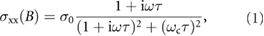
where  is the zero-field conductivity,
  , where f is the microwave frequency,
  the lifetime of the charge carriers and
  the cyclotron frequency. Here e is the elementary charge,
  the effective mass of the charge carriers and B the applied magnetic flux density. The microwave absorption A is proportional to the real part of the (optical) conductivity

Hence  is the measured quantity in microwave absorption experiments. In order to observe the quantum behavior of a system there are several conditions which must be fulfilled [26, 48]. First, the magnetic field must be strong enough to fulfill the quantization condition
  leading to quantization of the density of states into Landau levels, that give rise to field-induced oscillations in the conductivity. Here
  is the single particle life-time. This condition can be understood as a requirement for the charge carrier to carry out at least one full classical cyclotron orbit without scattering. Also the charge carrier temperature T must be small compared to the spacing between the Landau levels
  to prevent thermal damping of the signal. Since these measurements are performed on large area samples, the width of the charge carrier density distribution
  should be much smaller than its mean value
  ,
,  . In contrast to Hall measurements, for a detectable spectroscopic signal the additional condition of
  , where
  is the transport scattering time, is required. This can be classically understood as the necessity for at least one scattering event during one cycle of the microwave oscillation [26].
The SdH oscillations are described by the general Lifshitz–Kosevich-formula (LK) in the limit of low temperatures in spite of the non-equidistant Landau level spacing due to the linear energy dispersion in graphene [26, 48, 49]. Since the microwave absorption  is directly proportional to the real part of the conductivity
  the microwave absorption detected SdH is described by
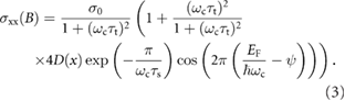
Here  is the Fermi energy of the system,
  the reduced Planck constant and
  is Berry's Phase (modulo 2
 ). By inverting the conductivity tensor the expression for SdH oscillations in the resistivity domain is found:
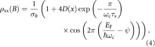
In both cases  accounts for the temperature damping:
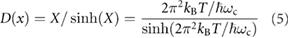
with the Boltzmann constant  and the absolute temperature T. The quantum mobility
  of the sample can be determined by evaluation of the amplitude of the oscillations [26, 48]. In case of the electrical measurements the expression
can be derived, from equation (4). Here the fitting parameter f summarizes any other non-oscillatory contribution, such as geometrical scaling factors and zero field resistance. For the case of microwave absorption measurements the derivation from equation (3) leads to
Here the fitting parameter  counts not only zero-field conductivity but also for microwave absorption specific parameters, such as effective microwave field strength experienced by the sample.
The temperature-independent charge carrier density  can be extracted from the oscillation period by:
where  and
and  are the spin- (
 ) and valley-degeneracy (
 ) in graphene and
  the oscillation period in the inverse field. Due to the linear energy dispersion, the Fermi energy
  is directly related to the charge carrier density by

where  is the Fermi velocity
  [14].
[14].
Since in our measurements a relatively large area of 
 is investigated every parameter should be taken in a first approximation as average over the sample and can indicate therefore the sample quality in terms of uniformity. The obtained parameters represent the intrinsic properties of the sample only in the limit of highly isotropic and homogeneous samples.
4. Results
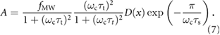
Figure 2 shows the microwave absorption and Hall measurements taken simultaneously. The resistance is measured by transport measurements using a Hall configuration (figure 2(a)), on the other hand in microwave absorption measurements were performed with a 20 G field modulation and hence the first derivative of the conductivity was obtained (figure 2(b)).

Figure 2. Measurements of the sample were carried out simultaneously at a bath temperature of  , a microwave frequency of
  , a modulation Field of
  and an excitation current of
  . The black curves represents the measured data set and red the symmetrized data used for evaluation. (a) Hall measurement of the sample. (b) The microwave absorption measurement; since field modulation is used, the derivative of the absorption signal is measured. (c) The optical absorption of the sample obtained by integrating the spectrum in panel (b).
Download figure:
Standard image High-resolution imageIn both, microwave absorption and Hall measurements, different transport phenomena were observed. The most important one in our measurements are the dominant SdH oscillations, which manifest as oscillations at fields above  in the Hall and the microwave absorption measurement. To our knowledge, this work is the first report of SdH oscillations by microwave absorption measurements of graphene. The oscillations were detectable up to frequencies of
  (compare supplementary information figure 7) in the microwave absorption measurement, where the low intensity of excitation microwave power leads to a low signal-to-noise ratio. Additionally in microwave absorption, electron paramagnetic resonances (EPR) can be detected. In our particular measurements the EPR signal of vanadium, used for doping of the substrate, is visible near B = 11.5 T [50, 51]. Additionally, at
  T weak localization manifests in the hall measurements as a small increase in the resistance and in microwave absorption measurements as a small signal increase [28].
The microwave absorption data was integrated to yield the absorption A (the conductivity), which is directly comparable to the theoretical model, equation (3) (figure 2(c)). Because of inhomogeneities and disorder in the sample and the large dimensions of the Hall bar  /
/ and
and  /
/ are mixed in the measurements. The data was therefore symmetrized in order to separate both contributions (see supplementary information, [52]). Another manifestation of the large area properties is a V-shape background in the Hall measurements instead of the flat background expected from equation (4) [13]. The mean value of the envelopes of the oscillations was subtracted to remove the background (see supplementary information).
We use a formula for resistivity  equation (4) and conductivity
  equation (3) to describe SdH oscillations in transport and microwave absorption, respectively. The minima in conductivity (microwave absorption), correspond to minima in resistivity (diagonal component of the inverse conductivity tensor), as observed in the experimental data, figures 2(a) and (c). The correspondence is due to large Hall resistivity
  ,
,  , which enables inversion of the tensor. Due to the approximation,
  assuming monotonic B-dependence of
  (no oscillations) and
  , we get the proportionality between oscillatory contribution to conductivity
  and resistivity
  ,
,  .
.
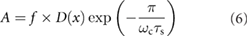
The temperature dependence of the SdH oscillations is illustrated in figures 3(a) and (b). The SdH oscillations are clearly visible up to  . The background is temperature independent in both measurements. A plot of the Landau level index over the inverse field is shown in figure 3(c). Using the slope, the charge carrier density was calculated by using equation (8) and shows
  for both measurements at
  , which translates to
  ; repeating the analysis for higher temperatures (not shown) reveals a similar value. The magnitude and lack of temperature dependence of
  is similar to prior reports for hydrogen intercalated monolayer graphene [39, 53]. We extrapolate the linear fit in figure 3(c) to
  to determine the Berry's phase. We obtain
  from both transport and optical measurements. This is close to the expected value of
  and indicates that the sample is predominantly MLG, since BLG would have a Berry's phase of
  . A plot of the fast-Fourier-transformation of the SdH oscillations is shown in figure 3(d) and shows one major signal at an oscillation period of B = 91.7 T and thus using equation (8) a charge carrier density of
  and a small harmonic at approximately doubled frequency. The results confirm that the Fermi energy and Berry's phase are independent of the measurement technique used and that only MLG contributes to the SdH oscillations.
Figure 3. Temperature dependent transport measurements. The measurements were carried out at a microwave frequency of  , modulation Field
  and excitation current of
  . Hall measurements are red and microwave absorption measurements black. (a) Temperature dependence of the microwave absorption conductivity. The data is normalized and offset for clarity. (b) Hall measurements show the same trends as the microwave absorption measurements. The data is normalized and the offset shifted for clarity. (c) Landau-Fan plot of the positions of the minima of the SdH oscillations in both measurements at a bath temperature of
  . The inset shows the intercept of about 0.5. (d) Fast-Fourier-transformation of the SdH oscillations at the same temperature. The data is normalized and offset for clarity. (e) Temperature dependence of the charge carrier temperature. At temperatures T < 15 K the charge carrier temperature decouples from the bath temperature due to joule heating when the current is
  A. A Hall measurement with only
  at 2.3 K is marked as blue dot and is close to the expected charge carrier temperature (light blue line).
Download figure:
Standard image High-resolution image
While in the Hall measurements only the single particle life time  contributes to the amplitude of the oscillations, in case of microwave absorption measurements also the transport lifetime
  plays a role. Because there is no accurate measurement of
  in this particular sample it was assumed to be
  , as in ordinary metals and semiconductors. With this assumption the mobility extracted from equation (7) is an upper limit, which is a useful quantity for comparison. The ratio
  is reportedly favored in graphene because backscattering is forbidden. However, a crossover to the ordinary behavior
  is possible at low carrier densities (
 ) [54, 55].
The mobility is assumed to be temperature independent throughout the data analysis, as observed experimentally in intercalated samples [39, 49]. A self-consistent fit of the temperature dependence of the SdH oscillations is used to obtain the electron temperature. The electron temperature is then plotted as a function of the bath temperature in figure 3(e). As is readily seen, the carriers become hotter than the bath for  . We believe that the joule heating from the Hall current of
  coupled with insufficient heat extraction from the lattice, caused the deviation in electron temperature. To test this, we reduced the Hall current to
  and found an improvement. The electron temperature became T = 4.8 K when the bath temperature is T = 2.3 K; this is also plotted in figure 3(e). In case of the microwave absorption measurement the used microwave frequency
  causes the heating of the charge carriers (compare supplementary information figure 7). The fit of equation (6) to the SdH Hall data for
  yields a quantum mobility of
  and the fit of equation (7) to the microwave absorption data for
  yields
  . Since the ratio of
  is unknown, there is uncertainty in the latter measurement. Therefore, the estimated mobilities for the microwave absorption measurements represent the upper limit.
Despite the fact that essentially the same graphene area is probed by both measurement methods, the microwave absorption measurements show lower mobilities than the Hall measurements. The difference in mobilities can be understood as a consequence of inhomogeneities, which were anticipated given the Hall and Raman data taken before the sample was patterned into a bar. The Hall measurement is preferentially sensitive to favorable conduction channels between the electrodes and tends to favor the highly conductive parts of the sample.
In microwave absorption measurements the whole sample contributes equally to the resulting signal, because the microwave field induces electronic oscillations only in length scales of  m [29]. In Hall measurements the induced driving field is in the range of the distance betweens the contacts (here mm). This difference becomes in particular important in samples with inhomogeneities, since different spatial parts of the samples may contribute different to the conductivity. This conclusion is also supported by large ratio of horizontal
  and vertical
  resistance
  measured in van der Pauw configuration taken before the sample was patterned into a bar.
We note that, in addition to inhomogeneities, the spectral dependence of the scattering mechanisms could also lead to a minor difference between the quantum mobility determined by optical absorption, which probes electron–hole excitations in the vicinity of the Fermi level and by transport measurements, which probes single-charge carries at the Fermi level. However, this effect will be of minor importance in our relatively highly doped ( ) samples.
The different processes of carrier heating could also cause the difference between the two mobilities. The optical absorption will lead to significant heating at low temperatures only ( ), and, as we have shown (see figure 3(e), also compare supplementary information figure 7). Joule heating can be neglected at
  . As we have excluded the
  data from the analysis of the quantum mobility, the role of inhomogeneities in different spatial parts of the graphene sheet probed by either experimental technique is the major contribution to the observed discrepancy.
5. Summary
We report extensive comparative transport studies of large area, single layer hydrogen intercalated graphene measured simultaneously by two methods: Contacted using a large area Hall bar and contactless microwave absorption from the bar. Shubnikov–de Haas oscillations are exhibited by both methods up to 53 K. The sheet density determined by both methods were within experimental error, showed minimal temperature dependence, were consistent with room temperature Hall measurements of the sample before bar fabrication and are consistent with electronic transport measurements by others using the Hall effect. Further analysis of the SdH oscillations produced by both methods yielded a Berrys phase of 0.45 (modulo 2 ), consistent with monolayer graphene. The mobility found by microwave absorption measurements was about two-fold less than the mobility found in Hall measurements. The difference is most likely due to sample inhomogeneity, where the Hall measurements tend to overestimate the conductance along favorable conduction channels in contrast to the microwave absorption measurements which obtain contributions from all regions of the sample. This work demonstrates microwave absorption as a valuable characterization technique with the potential for use in the production environment for graphene, or similar materials. This is due to the contactless nature of the method, which greatly simplifies the measurement process and the critical characterization data produced.
Acknowledgments
Financial support by the Deutsche Forschungsgemeinschaft under project DFG: NE1900/2-1, SPP1601 NE1900/3-2 and SL104/3-2 is gratefully acknowledged. Also financial support from the Czech Science Foundation under project 16-15763Y and Ministry of Education, Youth and Sports of the Czech Republic through the project CEITEC 2020 (LQ1601) is gratefully acknowledged. Work at NRL was supported by the Office of Naval Research.