

Abstract
The charge transfer phenomenon is identified to be a major factor determining exciton and trion characteristics of atomically thin MoS2 layers in various stacking configurations. We report photoluminescence (PL) from CVD-grown layered MoS2 in the presence of a skewed or a deformed triangular-shaped monolayer/bilayer (1L/2L) lateral interface. Integrated PL mapping images over the 1L and 2L MoS2 regions revealed that the neutral exciton emission was significantly enhanced and exhibited an oscillatory behavior in its intensity in the 1L region near the 1L/2L boundary, whereas the negative trion emission remained unchanged. The interplays among the number of MoS2 layers, a substrate, and a geometric boundary structure of the 1L/2L lateral interface turned out to be important in charge transfer due to a modulation in work functions. Density functional theory predicted that the work functions of 1L and 2L MoS2 were strongly influenced not only by the substrate material but also by the edge configuration of MoS2. As a result, PL intensity profiles showed rich features such as a stacking dependent decomposition of excitons and trions, a sharp spectroscopic contrast along the 1L/2L boundary, and a charge transfer relevant to the work function difference at the lateral interface. Our results demonstrate that understanding the MoS2 PL is useful in characterizing the electronic properties in 2D layered nanostructures and sheds light on possible new device applications.
Export citation and abstract BibTeX RIS
Introduction
Atomically thin two-dimensional (2D) transition metal dichalcogenides (TMDs), such as molybdenum disulfide (MoS2), exhibit a noticeable change in the electronic band structure from an indirect bandgap in bulk to a direct bandgap in monolayer (1L) [1, 2]. Owing to the modifications in the electronic structures as a function of the layer number (N), a few-layer MoS2 (1 ⩽ N ⩽ 4) has a great potential for optoelectronic devices such as phototransistors [3–6], solar cells [7], and light emitting sources [8]. In a few-layer MoS2, two distinct optical transitions are observed at ~1.85 eV (A exciton) and ~2 eV (B exciton) [1], which originate from the valence band splitting at the K point of the Brillouin zone due to the spin–orbit coupling and the interlayer interaction [2, 9]. In MoS2, unintentional n-type doping can be caused by sulfur vacancies [10], PMMA or acetone used in a transfer process [11], and charge traps at the interface between MoS2 and SiO2 substrate [12]. As a result, an excess electron can be tightly bound to a neutral exciton (X), forming a negatively charged exciton (X−) [13, 14]. As both the neutral excitons and the negatively charged excitons (also known as negative trions) are closely related to the optical transitions of MoS2, understanding their characteristics is one of the important issues not only for optoelectronic applications but also for fundamental research works.
Optical responses of excitons and negative trions in 1L MoS2 are strongly influenced by the carrier density. For example, spectral weights of the absorption and photoluminescence (PL) responses of the excitons can be systematically increased with decreasing electron doping density via back-gate voltage, whereas those of the negative trions are nearly unchanged [13]. When the excess electrons of unintentionally n-doped 1L MoS2 are extracted by the adsorption of chemical p -type dopants, trion formation rate from excitons decreases, resulting in the enhancement in the PL spectral weight of the X peak [15]. In contrast, the PL spectral weight of the X peak is reduced by the adsorption of chemical n-type dopants [15]. Without the external extraction or injection of electrons, charge transfer can also occur in the 'vertically stacked' TMD heterostructures, resulting in the variations of the PL intensities of the X and X− peaks in the constituent TMD layers [16, 17]. For example, in the vertically stacked MoS2/WS2 bilayers, charge transfer occurs from WS2 to MoS2 owing to the type-II band alignment, resulting in an increase of the PL intensity of the X− peak in MoS2 [16]. The difference in work functions of constituent TMD materials also leads to charge transfer. For example, a work function difference across the 'lateral' WS2/MoS2 heterojunction induces the electrical potential distribution and, in turn, initiates the charge transfer between WS2 and MoS2 [18, 19]. The work functions are influenced by several factors: layer thickness, surface chemistry, underlying substrate, and edge termination type [20, 21]. The charge transfer can occur even at the lateral homojunction of monolayer and multilayer MoS2, resulting in an enhancement of the photoresponse [22]. The space charge region induced by the charge transfer at the 2D lateral junction extends to a much longer distance than that in a bulk junction [18, 19, 23, 24]. Because the PL responses of layered TMDs are sensitive to the variation of the electron density and the number of atomic layers, PL mapping images of the X and X− peaks can provide useful information on the charge transfer across the lateral interface and the space charge region over the area around the lateral interface of the layered TMDs.
In this paper, we report simultaneous studies of spatially resolved Raman scattering and PL from a few-layer MoS2 in which 1L/2L lateral interface is formed. In particular, PL mapping images revealed that spectral intensities of the excitons were greatly enhanced in the 1L region near the lateral interface between 1L and 2L MoS2, whereas those of the negative trions were nearly unchanged. To understand the exciton and trion emission behaviors near the 1L/2L lateral interface, we used density functional theory (DFT) to calculate work functions for 1L and 2L MoS2 on a SiO2 substrate. Furthermore, we calculated work functions for different types of edge terminations of 1L and 2L MoS2 and compared the DFT calculations with the experimental PL results.
Results and discussion
The morphology of the multilayer-stacked MoS2 was identified by optical microscopy, atomic force microscopy (AFM), and Raman spectroscopy. Figure 1(b) shows an optical microscope image of the deformed triangular-shaped MoS2 flakes on the SiO2 substrate. The multilayer-stacked MoS2 exhibits a change in brightness contrast due to the thickness variation. The AFM height image in figure 1(c) reveals that the co-centered triangular-shaped MoS2 is stacked layer by layer on the large 1L MoS2. The lateral size of each co-centered MoS2 becomes smaller and smaller with an increase of the number of layers. Note that the 1L/2L lateral interface exhibits a deformed triangular shape boundary composed of the skewed edges. AFM line scan profiles show that the thickness of the 1L MoS2 on the SiO2 substrate and that on the MoS2 are ~12 Å and ~9 Å, respectively. These values are in good agreement with previously reported ones [25, 26]. The bright center in the AFM image corresponds to bulk MoS2 with a thickness of ~50 nm.
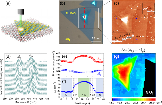
Figure 1. (a) Schematic illustration of the 1L and 2L MoS2 on SiO2. (b) Optical microscope image of the multi-stacked MoS2. (c) Tapping-mode AFM topographic image of MoS2 obtained over the area marked by the square box in the optical microscope image. Upper right inset shows an AFM line scan profile of the 1L MoS2 on the SiO2 substrate. Lower left inset shows an AFM line scan profile of the multi-stacked MoS2 on the 1L MoS2. (d) Series of Raman spectra along the dashed arrow in the optical microscope image. Each spectrum was normalized to the peak value of the  mode. (e)
  and
and  phonon energy changes and (f) corresponding Δω along the dashed arrow in the optical microscope image. (g) Spatial variations in the energy difference Δω between the
  and
and  phonon modes.
Download figure:
Standard image High-resolution imageOptical phonon energies in MoS2 vary as a function of N. Figure 1(d) shows a series of the Raman spectra along the dashed arrow in the optical microscope image. Two distinctive Raman peaks are observed:  and
and  phonon modes, corresponding to the in-plane and out-of-plane vibrational modes, respectively [25]. As the number of layers increases, the
  phonon energy shifts downward from 385 cm−1 for N = 1 to 383 cm−1 for bulk, while the
  phonon energy shifts upward from 404 cm−1 for N = 1 to 409 cm−1 for bulk. These shifts in their phonon energies are mainly due to the changes in the short-range interlayer and the long-range Coulomb interactions with an increase in the number of layers [27]. The difference in the peak energies
  identifies the number of layers (figure 1(f)): 19.36 ± 0.08, 22.20 ± 0.14, 23.33 ± 0.57, and 24.53 ± 0.21 cm−1 for N = 1, 2, 3, and 4, respectively. For bulk MoS2 at the center region,
  25.79 ± 0.09 cm−1. The
  image in figure 1(g) clearly visualizes the vertically stacked MoS2 layer by layer and is comparable to the AFM data. The values of
  are in excellent agreement with previously reported ones for mechanically exfoliated MoS2 [25, 26] and chemical vapor deposition (CVD)-grown MoS2 [28, 29].
To explore the exciton and trion emission properties related to the changes in the band structures of 1L, 2L, and a few layers of MoS2, spatially resolved PL measurements were performed over the same area where the AFM and Raman images were obtained. Figure 2(a) shows an image of the spectral weight of the A exciton (IA) obtained over the area shown in figure 1(c). Emission efficiency of IA decreases when the layer thickness increases from 1L to a few layers. The PL response is finally quenched in thick MoS2 for N > 5. A remarkable feature observed in the PL mapping image is that IA is significantly enhanced in the 1L MoS2 region near the 1L/2L lateral interface, identifying a sharp spectroscopic contrast between 1L and 2L MoS2. Furthermore, the enhancement in IA strongly oscillates in its intensity around the 1L/2L boundary.
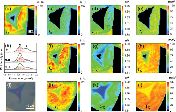
Figure 2. (a) Spectrally integrated PL intensity image of the A (X + X−) exciton region. (b) Representative PL spectra obtained from 1L MoS2 remote from the 1L/2L interface (1L-1), 1L MoS2 near the interface (1L-2), and 2L MoS2 (2L). Probing spot for each spectrum is marked in figure 1(c). In 1L MoS2, the A exciton region is decomposed into the negatively charged exciton (X−) peak and the neutral exciton (X) peak. (c)–(e) are PL integrated intensity, peak energy, and linewidth maps of the X− peak, respectively. (f)–(h) are PL integrated intensity, peak energy, and linewidth maps of the X peak, respectively. (i) Optical microscope image of MoS2, consisting of only 1L and 2L. (j)–(l) are PL integrated intensity, peak energy, and linewidth maps of the X peak, respectively. All of the image sizes are 40 × 40 µm2.
Download figure:
Standard image High-resolution imageThe PL spectrum obtained from 1L MoS2 consists of the A exciton and the B exciton that originate from the direct gap transitions at the K point [1]. The A–B splitting comes from the valence band splitting mainly due to the spin–orbit coupling [2, 9]. For 2L MoS2, the interlayer interaction also contributes to the valence band splitting [2, 9]. In the case of the unintentional n-doping in MoS2, excess electrons can contribute to the formation of negative trions consisting of two electrons and one hole [13]. Because of the large trion binding energy of ~40 meV in 1L MoS2 [14, 15, 30, 31], the trions are present in 1L MoS2 at room temperature. In contrast, in 2L MoS2, as the conduction band minimum occurs at the Λ point lying between the K and Γ points, the photo-excited electrons can be easily relaxed to the Λ valley via thermal escape from the K-point valley at room temperature, leading to a significant decrease of the trion emission [32]. As a result, in 2L MoS2, only the exciton emission becomes a dominant process in the K–K transition, whereas the trion emission at the K point is considerably suppressed [14]. Figure 2(b) shows the representative PL spectra obtained from 1L MoS2 remote from the 1L/2L interface (marked by 1L-1), 1L MoS2 near the interface (marked by 1L-2), and 2L MoS2 (marked by 2L). In the 1L MoS2, the spectral region of the A peak is decomposed into two Lorentzian peaks, consisting of the X and the X− peaks. The PL spectra obtained from 1L MoS2 are well reproduced with the sum of these two peaks and the B exciton peak, while the PL spectra in 2L MoS2 consist of only the X and the B components. The spectrally integrated intensity, peak energy, and linewidth maps of the X− and the X peaks are shown in figures 2(c)–(h). Note that the band-to-band PL transition of the trions at the K point occurs only in 1L MoS2 at room temperature. Thus, the trion emission is negligible in the other MoS2 region for N ⩾ 2, designated by black colors in figures 2(c)–(e). Interestingly, figures 2(c) and (f) show that  is spatially inhomogeneous and strongly enhanced near the 1L/2L lateral interface in the 1L region, whereas
  is relatively uniform. Therefore, the strong enhancement in IA in the 1L MoS2 region is mainly attributed to the enhancement in
  . For N ⩾ 2, there is no appreciable change in
  . Finally, the exciton emission is quenched for N > 5.
The average peak energies of the negative trions ( ) and neutral excitons (
 ) obtained from the region enclosed by the dashed squares in the peak energy maps in figures 2(d) and (g) are 1.808 ± 0.002 eV and 1.843 ± 0.003 eV, respectively, giving rise to the trion binding energy of ~35 meV, which is consistent with the previously reported values of mechanically exfoliated [14, 15] and CVD-grown 1L MoS2 [30, 31]. Distinctive difference in
  is clearly observed in the exciton transitions at the K point of the Brillouin zone as the number of layers are increased:
  decreases to 1.837 ± 0.005 eV and 1.824 ± 0.001 eV for N = 2 and 3, respectively. The decrease in
  with an increase of the layer thickness is partly due to the relaxation of size confinement [33, 34]. In addition to the changes in the peak energies of the excitons, the average spectral widths of the excitons (
 ) are also affected by layer numbers:
  decreases systematically from 99.3 ± 2.5 meV to 95.2 ± 3.4 meV and to 82.4 ± 2.2 meV for N = 1, 2, and 3, respectively.
The MoS2 sample shown in figure 1(b) consists of multi-stacked layers. Therefore, the electronic correlation between the 1L and 2L MoS2 might be altered in the presence of MoS2 for N ⩾ 3. To understand the exciton and trion characteristics related only to the 1L/2L lateral interface more precisely, PL mapping measurement was performed on the other sample consisting of only 1L and 2L MoS2 (figure 2(i)). Figures 2(j)–(l) show the intensity, energy, and linewidth maps of the X peaks for the 1L and 2L MoS2 with a deformed triangular shaped 1L/2L lateral interface. Similarly to the previous result, the X peak intensity is substantially enhanced in the 1L MoS2 region near the 1L/2L interface, whereas  in the 2L region does not exhibit any noticeable changes. Besides, the energy and the linewidth of the X peak are decreased in 2L MoS2. The average values of the X peak energies are 1.844 ± 0.009 eV and 1.817 ± 0.004 eV for 1L and 2L MoS2, respectively. The variations in the X peak energies between two different MoS2 samples for N = 2 are presumably due to the differences in interlayer twist angles, shapes, and/or stacking configurations between 1L and 2L MoS2 [35, 36].
Figures 2(f) and (j) show that the PL signals exhibit some distinct features such as strong enhancement and oscillation of  in the vicinity of the skewed/deformed outer edge of 2L MoS2. The spatial variation in
  seems to be attributed to the electrostatic potential difference because it affects the sensitivity of PL response. For example, electrochemical control of PL was reported in the case of a MoS2 flake, suggesting that the electrostatic potential can influence the overall strength of PL of MoS2 [37]. According to the surface potential study of MoS2/SiO2 using Kelvin probe force microscope, the work function (
 ) of 1L MoS2 is smaller than that of 2L MoS2 by 0.05 eV [38]. Therefore, to explain the spatial variation in
  , we may consider the electron transfer from 1L to 2L MoS2 across the 1L/2L lateral interface owing to the work function difference. The decrease in the number of excess electrons in 1L MoS2 suppresses the trion formation rate, resulting in the enhancement of the exciton PL intensity. Our experimental observation is consistent with the results of the changes in
  and
and  in 1L MoS2 when the number of excess electrons are decreased via back-gate voltage in the field-effect transistor structure and when p -type dopants are adsorbed onto 1L MoS2 [13, 15, 39]. The strongly enhanced
  and the relatively unchanged
  with the decrease of the excess electrons can be theoretically explained by solving the rate equations within the framework of a three-level model in a steady-state condition [15]. Based on the three-level model consisting of an exciton, a trion, and the ground state, the exciton PL intensity is strongly enhanced with a decrease of the electron density, whereas the trion intensity is relatively insensitive to the change in the electron density [15]. The 1L MoS2 region near the 1L/2L boundary might be strained due to the presence of the 2L MoS2, resulting in the changes in the neutral exciton peak position and intensity. The in-plane
  phonon mode is sensitive to strain and shifts in energy linearly at a rate of −5.2 cm−1/% for biaxial strain [40]. The average
  phonon energies are 384.1 ± 0.1 cm−1 and 384.3 ± 0.2 cm−1 in the 1L MoS2 region near and away from the 2L boundary edge, respectively. The peak energy difference of 0.2 cm−1 corresponds to a strain of ~0.038%. The exciton PL peak position and intensity changes are negligible under such a small strain [40].
Considering the charge transfer across the 1L/2L lateral interface due to the work function difference, the strong oscillation of  in the vicinity of the 'skewed' or 'deformed' triangular-shaped 1L/2L lateral interface is not observed in other types of MoS2 homostructures with a CVD-grown 'equilateral' triangular-shaped 1L/2L lateral interface and a mechanically exfoliated 'flat' 1L/2L interface [41, 42]. Figure 2(f) shows that the oscillation of electrostatic potential in the vicinity of the skewed edge is evident. The work function depends appreciably on a straight edge that comprises the oblique edge boundaries. Furthermore, the work function in MoS2 depends on the edge termination atoms [21]. Indeed, Wei et al has reported that the work functions of TMD edges with different edge terminations should be taken into account in order to understand charge transfer behaviors in the lateral heterostructure of TMDs [21].
To understand charge transfer characteristics in more detail, we performed theoretical calculations of work functions of 1L and 2L MoS2 based on the DFT. The work functions are calculated to be 5.34 eV and 4.97 eV for the 1L and 2L MoS2, respectively (figure 3(a)). However, our experiments were performed on the MoS2 layers on the SiO2 substrate with possible exposure to H2O during the transfer process. In order to include the effect of the substrate, we calculated work functions and charge density isosurfaces for two MoS2 1Ls, with an atomically thin SiO2 layer (thickness ~6 Å) and H atoms inserted between the 1Ls. Similarly, we also calculated work functions and charge density isosurfaces for two MoS2 2Ls, with the SiO2 layer and H atoms inserted between the MoS2 2Ls. From the charge density isosurfaces in figures 3(b) and (c) we infer there are more S-Si interactions in 2L MoS2/SiO2 than in 1L MoS2/SiO2. Interestingly, the order of the calculated work functions is reversed: Φ = 4.52 eV and 4.67 eV for the 1L and the 2L MoS2 with the SiO2 layer and H atoms, respectively. The difference in the work functions allows us to interpret the overall features of the PL maps in the 1L MoS2 region around the 1L/2L lateral interface. To equilibrate the Fermi energies, transfer of electrons from the 1L to the 2L MoS2 should take place across the step boundary. The transfer of electrons from the 1L to the 2L MoS2 leads to an enhancement in  in the 1L MoS2 region near the 2L MoS2 flake. However, the transfer of electrons will not affect
  in the 2L MoS2 region because the conduction states near the K points are mostly empty.
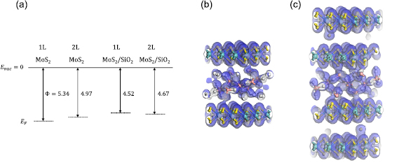
Figure 3. Work functions and charge density: (a) calculated work functions of 1L and 2L MoS2 surfaces with and without SiO2 substrates. Charge density isosurfaces of (b) 1L MoS2/SiO2 and (c) 2L MoS2/SiO2. Turquoise, yellow, pink, light gray, and white spheres correspond to Mo, S, Si, O, and H atoms.
Download figure:
Standard image High-resolution imageThe PL characteristics are also influenced by a termination atom of the 1L MoS2 flake on the basal 1L MoS2. S terminal atoms tend to gain electrons and Mo terminal atoms tend to lose them because the electronegativity of the S atom is larger than that of the Mo atom. The negatively charged S-termination exerts Coulomb force away from the termination on the electrons in the vicinity. Likewise, the positively charged Mo-termination exerts the force towards the termination on the electrons. Therefore, the S-termination weakens the enhancement effect of  in the 1L MoS2 region near the 1L/2L lateral interface, whereas the Mo-termination strengthens the effect.
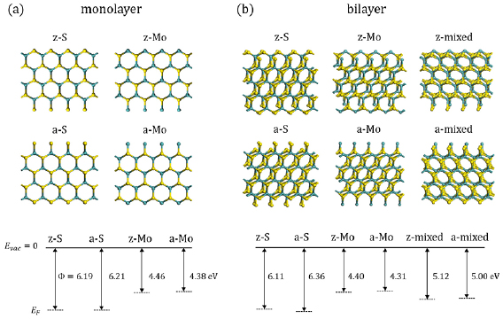
To assess the enhancement effect of  in terms of electronic energies, we calculated work functions for various edge terminations of MoS2. Experimentally, Mo-terminated zigzag edges and S-terminated antenna edges have been observed in 2L MoS2 boundary edges on 1L MoS2, indicating that various edge structures can be formed via CVD growth [43]. In general, four different types of edge terminations can be considered for the 1L MoS2, as shown in figure 4(a): a zigzag edge with S termination (z-S), a zigzag edge with Mo termination (z-Mo), an antenna edge with S termination (a-S), and an antenna edge with Mo termination (a-Mo) [44]. We included a pair of symmetric MoS2 strips in a supercell to accurately calculate work functions of different terminations of MoS2. The zigzag (antenna) terminations have edge atoms forming zigzag-shaped (antenna-shaped) arrays. S-termination and Mo-termination indicating outer edge atoms correspond to S and Mo, respectively. In the cases of 2L MoS2, we additionally considered the mixed terminations whose outer edge atoms are both S and Mo (figure 4(b)).
Figure 4. (a) Schematics of the top views of the zigzag and antenna edges of MoS2 1Ls with the S- and Mo-terminations, and the corresponding work functions. (b) Schematics of the zigzag and antenna edges of MoS2 2Ls with the S-, Mo-, and mixed-terminations, and the corresponding work functions.
Download figure:
Standard image High-resolution image
The computed work functions are summarized in figures 4(a) and (b) for 1L and 2L MoS2, respectively. The work functions of S-terminations of 1L MoS2 are 6.19 eV (6.21 eV) for the zigzag edge (the antenna edge), and those of 2L MoS2 are 6.11 eV (6.36 eV) for the zigzag edge (the antenna edge). Similarly, the work functions of Mo-terminations of 1L MoS2 are 4.46 eV (4.38 eV) for the zigzag edge (the antenna edge), and those of 2L MoS2 are 4.40 eV (4.31 eV) for the zigzag edge (the antenna edge). Interestingly, the work functions of mixed terminations of 2L MoS2 are 5.12 eV (5.00 eV) for the zigzag edge (the antenna edge), which are in between the work functions of S-terminations and those of Mo-terminations. Our calculated work functions indicate that the electronic potential away from the edge depends strongly on the types of the outer edge atoms (S or Mo atoms), but weakly on the zigzag and the antenna types of the same species. The calculated work functions of the 1L and 2L MoS2 are larger for the S-terminations and smaller for the Mo-terminations as expected in terms of the electronegativity of the S and Mo atoms. The calculated work functions confirm our claim that the S-termination weakens the enhancement effect of  in the 1L MoS2 region near the 1L/2L lateral interface, whereas the Mo-termination strengthens the effect.
In the case of a MoS2 flake with a skewed/deformed triangular shape, outer atom configurations and edge types may vary, and the electron density at the boundary of the skewed/deformed triangle (i.e. the 1L/2L interface) is expected to be highly non-uniform. The non-uniform electron density at the 1L/2L interface and the corresponding transfer of electrons from the 1L MoS2 to the 2L MoS2 lead to the varying effect of  in the 1L MoS2 region near the MoS2 flake (i.e. 2L MoS2). The irregular shape and large change of PL around the 1L/2L lateral interface is consistent with our calculated work functions. The enhanced area of
  in the 1L MoS2 region extends more than 10 µm (figures 2(f) and (j)). Theoretical studies show that the depletion width of the 2D lateral junction extends much longer than that of the bulk counterpart [23, 24]. For example, Kelvin probe force microscopy of MoS2/WS2 heterojunction has revealed the depletion width of several micrometers [19]. Furthermore, the space charge region extends even longer beyond the depletion width [23]. Therefore, our experimental PL results clearly demonstrate that the space charge region spreads over the large area around the 2D lateral junction.
Conclusions
We performed Raman and PL mapping measurements simultaneously on the multi-stacked MoS2 to study optical phonons and exciton properties. The Raman mapping images helped identify the number of MoS2 layers, which was confirmed by the AFM measurement. Interestingly, a strong enhancement and an oscillatory behavior of the neutral exciton emission were observed in the 1L MoS2 region near the 1L/2L lateral interface. DFT calculations showed that the work function was significantly influenced by the underlying SiO2 substrate: it was lower in 1L MoS2 than in 2L MoS2, resulting in the electron transfer from 1L to 2L MoS2. Furthermore, the work function strongly depended on the terminal atoms of the MoS2 edge, leading to the non-uniform electrical potential distribution at the 1L/2L lateral interface. As a result, highly inhomogeneous exciton emission was observed in the 1L MoS2 region. Finally, our experimental and theoretical analysis of a TMD material demonstrates that the exciton and trion properties can be modulated by the type of the edge termination, providing diverse design strategies for 2D optoelectronic nanodevices.
Experimental methods
Synthesis of layered MoS2 film on SiO2
MoS2 was synthesized by using a CVD method. The growth method is as described in a previous report [28]. Briefly, a 50 nm-thick MoO3 film as molybdenum precursor was deposited on an Al2O3 plate by a thermal evaporator and sulfur powder was used as the sulfur precursor. To grow MoS2, two zone furnaces were utilized. A total of 0.5 g of sulfur powder was placed in an Al2O3 crucible and positioned at the center of heating zone 1. The grown SiO2 substrate was then placed face-down and parallel on the pre-deposited MoO3 film on Al2O3 (MoO3/Al2O3). The temperatures of both zone 1 (sulfur powder in crucible) and zone 2 (Si/SiO2/MoO3/Al2O3) were then increased at a rate of 15 °C min−1 to 180 °C and 680 °C respectively, and maintained for 30 min under argon atmosphere at a flow rate of 350 sccm. After growth, the furnaces were cooled rapidly by opening the chamber. The grown MoS2 was then transferred to a SiO2 substrate for optical measurements.
PL and Raman measurements
PL and Raman measurements were carried out in a backscattering geometry at room temperature. An Argon-ion laser with a wavelength of 514.5 nm was focused on the sample surface through an optical microscope objective (100×/0.9 NA) with a spatial resolution better than 1 µm. An excitation laser power was maintained at less than 0.5 mW to avoid any laser-induced heating effects. The scattered light from the sample was dispersed using a 150 or 1200 grooves mm−1 grating for PL or Raman measurements, respectively. The dispersed light was collected by a thermoelectrically cooled charge-coupled device detector. For the PL and Raman mapping measurements, the MoS2 sample was placed on a computer-controlled piezoelectric xy stage that moved in 1 µm increments along the x and y directions over the area of 40 × 40 µm2.
Theoretical calculations
The calculations were performed using the ab-initio total-energy and molecular-dynamics program VASP (Vienna ab initio simulation program) developed at the Institute für Materialphysic of the Universitat Wien, using the projector-augmented-wave approach [45]. The generalized gradient approximation (GGA) for the exchange-correlation energy functional was used [46]. We employed a plane-wave basis set for wave functions. The cutoff energy of the plane-wave basis set was 260 eV for structural relaxation calculations and 400 eV for all other calculations. We relaxed the lattice parameters and atomic positions, with the allowed remaining force on each atom less than 0.01 eV Å−1 for the structural relaxation calculations. We added a vacuum space larger than 19 Å between the MoS2 monolayers. The Monkhorst–Pack grid to sample the Brillouin zone was 24 × 24 × 1 to relax the 1L MoS2 unit cell, and to calculate the work functions of the 1L and 2L MoS2. The 5 × 5 × 1 Monkhorst–Pack grid was used to calculate the work functions of 1L and 2L MoS2 with SiO2 because we used 3 × 3 unit cell for 1L and 2L MoS2 in this case. The 21 × 1 × 1 Monkhorst–Pack grid was used to calculate the work functions for the zigzag/antenna edges with Mo-/S-terminations. Spin–orbit coupling was included in all calculations except for the structural relaxation calculations. The work functions are determined from the difference between the vacuum level and the Fermi level. It is well-known that band gaps are usually underestimated in GGA. However, the work functions calculated within GGA are more reliable than the band gaps calculated within GGA for the following reasons. First, unlike the band gaps, the Fermi levels and the vacuum levels are calculated without the explicit reference to the conduction band minima. Second, the vacuum levels and the Fermi levels are determined by ground state properties. We note that H2O molecules on MoS2 edges are adsorbed and dissociated easily [47]. The H atoms inserted between the MoS2 layers and SiO2 substrate possibly lead to hydroxyl groups (–OH), whose effects should be similar to those of the dissociated H2O. Indeed, after the structural relaxation calculation, some hydroxyl groups are formed in our calculations.
Acknowledgments
This research was supported by Basic Science Research Program through the National Research Foundation of Korea (NRF) funded by the Ministry of Education (Grant Nos. 2016R1D1A1B03935270 and 2016R1D1A1B04931384). SMK acknowledges support by Basic Science Research Program through the National Research Foundation of Korea (NRF) funded by the Ministry of Science, ICT and Future Planning (Grant No. 2018R1A2B2002859).