

Abstract
Semiconducting transition metal dichalcogenides (TMDs) demonstrate a wide range of optoelectronic properties due to their diverse elemental compositions, and are promising candidates for next-generation optoelectronics and energy harvesting devices. However, effective band offset engineering is required to implement practical structures with desirable functionalities. Here, we explore the pressure-induced band structure evolution of monolayer WS2 and Mo0.5W0.5S2 using hydrostatic compressive strain applied in a diamond anvil cell (DAC) apparatus and theoretical calculations, in order to study the modulation of band structure and explore the possibility of band alignment engineering through different compositions. Higher W composition in Mo(1−x)W(x)S2 contributes to a greater pressure-sensitivity of direct band gap opening, with a maximum value of 54 meV GPa−1 in WS2. Interestingly, while the conduction band minima (CBMs) remains largely unchanged after the rapid gap increase, valence band maxima (VBMs) significantly rise above the initial values. It is suggested that the pressure- and composition-engineering could introduce a wide variety of band alignments including type I, type II, and type III heterojunctions, and allow to construct precise structures with desirable functionalities. No structural transition is observed during the pressure experiments, implying the pressure could provide selective modulation of band offset.
Export citation and abstract BibTeX RIS
1. Introduction
Various types of two-dimensional (2D) materials have been heavily studied for diverse applications in nanoelectronics, flexible internet-of-things (IoT) devices, light-emitting/detecting devices, and/or energy harvesting devices [2–8]. Monolayer transition metal dichalcogenides (TMDs) are attracting interest due to their sizable direct band gaps [9–12]. Unlike single-element layered materials such as graphene [13], phosphorene [14, 15], or silicene [16, 17], the primitive unit cell of TMDs is composed of a transition metal (M = Mo, W, Re, Ta, Nb, etc) and two chalcogen (X = S, Se, Te) atoms, allowing for a wide range of compositional combinations. Their band structure, and hence their optoelectronic properties, vary with elemental composition from semiconducting to semi-metallic. The sulfide TMDs (MS2) are well suited for optoelectronic applications thanks to their relatively large band gaps, small effective masses, and high carrier mobilities [18, 19]. Moreover, the sulfides are known to be the most robust TMDs, chemically and mechanically, positioning them to be the most suitable 2D materials for practical applications [20, 21].
However superior their properties, the shortage of means to precisely and selectively engineer the band edges hinders realizing the spectrum of TMD-based electronic devices. Practical structures with desirable functionalities demand various types of band offsets or heterojunctions: (i) Type I heterojunctions, in which the band gap of a material is completely embodied within the band gap of the other (straddling gap); (ii) Type II heterojunctions, in which the band gaps of the two materials partially overlap (staggered gap); and (iii) Type III heterojunctions, in which the band gap of a material lies higher than the band gap of the other, leaving no overlap between the band gaps (broken gap; summarized in figure 4(d)). Many efforts have been made to progressively modulate the band offset beyond the natural compositional degree of freedom [11, 22–26]. Alloying of metals or chalcogens from the same valence group allows for continuous tunability of band structure with respect to the compositional ratio. Compositional engineering in Mo(1−x)W(x)S2 and MoS(x)Se(2−x) reportedly modulates their band structures, as well as effective mass and carrier transport properties [27–30]. Down-shifted band structures, as well as p-type MoS2 and MoSe2 behaviors, have been obtained by chemical doping of hole-donating Nb atoms [31, 32]. However, these methods lack the ability to arbitrarily control the band structures and band offsets, or to reverse the modulation.
Recent studies suggest that strain or pressure could be used to effectively modulate band structures and optoelectronic properties of 2D materials in a chemically clean, reversible, and precisely controllable manner [33]. For example, in-plane tensile strain applied on monolayer TMDs has been shown to reduce the optical band gap up to ~100 meV [34–36]. Moreover, monolayer MoS2 under out-of-plane compressive strain was reported to experience electronic transitions into indirect band gap semiconductor at 0.6 GPa, and into metal at 3 GPa, respectively [37]. 2D materials are especially responsive to hydrostatic pressure due to their unique layered geometry, as the interlayer van der Waals bond is highly compressible [38–43]. Application of hydrostatic pressure delivers compressive strains in in-plane and out-of-plane differently, which can help reveal unique physical phenomena of 2D materials in extremes. Under a given hydrostatic pressure, the interlayers bonded by van der Waals force are expected to be significantly influenced by compressive strain such that lattice distance is dramatically shortened and electronic interactions are significantly enhanced. On the other hand, the intra-layers with strong covalent bonds will be much less sensitive to the hydrostatic pressure. Multi-layered semiconducting TMDs were reported to undergo metallic transitions and orders of magnitude resistivity drop as well as the appearance of superconducting phase with increased pressure [39, 40, 42–48]. The direct band gaps of monolayer 1H–MoS2, MoSe2, and WS2 were reported to increase up to ~12%, ~9%, and ~5% under hydrostatic pressure, respectively [1, 49–51]. After direct-to-indirect band transition, the band gap of MoS2 is theoretically predicted to close at a much higher pressure of 68 GPa [39]. The large disparity in band gap behavior and transition pressures of the TMDs under hydrostatic pressure compared to uniaxial or out-of-plane compressive strain is likely a result of the different magnitude of the compressive strain applied onto different crystallographic directions. Moreover, MoS2-based field-effect transistors (FET) under hydrostatic pressure have been reported to have enhanced mobility, carrier concentration, and conductance [52]. In addition, charge transfer in MoS2/graphene heterostructures reportedly reduces the band gap of the MoS2 and shifts the Dirac point of graphene under hydrostatic pressure [41]. Charging effect from the pressure medium has been reported to induce difference in exciton intensities in monolayer MoSe2 under pressure [51].
In this light, we explore the pressure-induced evolution of band structures in monolayer transition-metal disulfides using a diamond anvil cell (DAC) in conjunction with theoretical calculations, and examine the possibility of pressure-induced band offset engineering. Monolayer 1H–WS2, 1H–Mo(1−x)W(x)S2 (x = 0.5 denoted as MoWS2, otherwise noted), and 1H–MoS2 were studied to explore the composition-dependence of band structure modulation.
2. Results and discussions
1H–WS2 single crystals with controlled monolayer thickness and lateral size reaching ~50 µm were synthesized by chemical vapor deposition (CVD) method (figure 1(a)) [53]. Various characterizations including high-resolution transmission electron microscopy (HRTEM), atomic force microscopy (AFM), resonant Raman spectroscopy, and photoluminescence (PL) spectroscopy indicated good crystallinity of CVD-grown monolayer crystals, comparable to that of exfoliated crystals (figure S1). The 1H–WS2 crystals with the growth substrate were cleaved and loaded into a diamond anvil cell (DAC) for pressure experiments (figure 1(b)). Monolayer 1H–MoWS2 was achieved by mechanical exfoliation of bulk MoWS2. Mo:W atomic ratio of 53:47 was confirmed using x-ray photoelectron spectroscopy (XPS) (figure 1(d)). According to previous reports, the distribution of Mo and W atoms are random in the aforementioned atomic range [27, 38, 54]. After initial inspections including optical, Raman spectroscopy, and PL spectroscopy a flake with high-quality monolayer region was selectively transferred onto a diamond culet of a DAC using PDMS stamp method (figures 1(e) and S2) [55]. Initial PL characterizations at ambient pressure showed strong and nearly symmetric peaks in both WS2 (figure 1(c)) and MoWS2 (figure 1(f)), indicating that the materials consist of high-quality crystals and have well-defined monolayer thickness. The direct optical band gaps at ambient conditions derived from the maximum point of the PL spectra were ~1.95 eV and ~1.90 eV for of the WS2 and MoWS2, respectively.

Figure 1. Preparation and characterizations of monolayer 1H–WS2 and 1H–MoWS2 samples for high-pressure experiments. (a) Schematic showing the chemical vapor deposition (CVD) synthesis setup for growing monolayer 1H–WS2. Insets are optical (left) and scanning electron microscopy (SEM; right) images of a representative monolayer 1H–WS2. Scale bars are 20 µm. (b) Optical images of a diamond anvil cell (DAC) with monolayer 1H–WS2 on a Si/SiO2 substrate. The white dashed line in the inset indicates the loaded region of WS2 and substrate. (d) X-ray photoelectron spectroscopy (XPS) spectrum of bulk 2H–MoWS2 sample. (e) Optical image of a DAC with an exfoliated MoWS2 flake on a piece of thin silicon wafer. White dashed squares indicate the region corresponding to the inset image, which shows the exfoliated flake including monolayer region with size of 5 µm × 20 µm. (c) and (f) Photoluminescence (PL) spectrum of (c) monolayer WS2 and (f) MoWS2 at ambient conditions before Ne gas loading.
Download figure:
Standard image High-resolution imageThe change in optical band gaps of the monolayer 1H–WS2 and 1H–MoWS2 under high pressure were evaluated from analysis of the measured PL spectra in situ. For 1H–WS2, a rapid increase in the direct band gap, as well as monotonic decrease in PL signal intensity were observed with increasing pressure. Analysis of the PL peak at 4.0 GPa indicated a band gap of 2.08 eV, but its intensity dropped below the noise level after 4.0 GPa, which implies a direct-to-indirect (D-to-I) band transition (figure 2(a)) [1]. 1H–MoWS2 alloy exhibited a similar pressure-dependent direct band gap increase to 2.05 eV at 6.1 GPa. The PL signal decreased and vanished above 6.1 GPa, which is attributed to the D-to-I band transition (figure 2(b)).
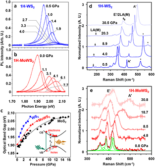
Figure 2. PL and Raman spectra evolution of monolayer TMDs with pressure (a) and (b) PL spectra of monolayer (a) 1H–WS2 and (b) 1H–MoWS2 at selected pressures. PL signal intensity dropped below noise level after 4.0 GPa and 6.1 GPa, for WS2 and MoWS2, respectively. (c) Optical direct band gap evolution of 1H–WS2, 1H–MoWS2, and 1H–MoS2 as a function of pressure. Solid lines are polynomial fits to the data. The band gap opening rates in linear regions of WS2, MoWS2, and MoS2 are 54 meV GPa−1, 36 meV GPa−1, and 25 meV GPa−1, respectively. (Inset) Schematic view of photoluminescence of monolayer TMDs with a direct band gap. CB, VB, and Eg indicate conduction band, valence band, and band gap, respectively. Experimental data of MoS2 were adapted from Nayak et al [1]. (d) and (e) Raman spectra of (d) WS2 and (e) MoWS2 at selected pressures. Asterisks denote silicon peaks. Green and black solid lines are Lorentzian fits and fit sum, respectively.
Download figure:
Standard image High-resolution imageAnalysis of the PL results, as well as results of MoS2 adapted from Nayak et al [1], are summarized in figure 2(c), presenting increase of direct band gap as a function of pressure, with different pressure dependence according to the different composition. The ambient band gaps range from 1.95 eV in WS2, 1.90 eV in MoWS2, and to 1.85 in MoS2, which are in good agreement with the previously reported composition-dependent band gap values [27]. The D-to-I transition pressures, attributed to the vanishing PL signal, ranged from 4.0 GPa for WS2, 6.1 GPa for MoWS2, and 16 GPa for MoS2. Interestingly, higher W composition led to a more pressure-sensitive direct band gap opening. The rate of WS2 was the fastest (54 meV GPa−1), which was more than double of that of MoS2 (25 meV GPa−1). The direct band gap opening rate of MoWS2 was an intermediate 36 meV GPa−1. The maximum direct band gap values before D-to-I transition remained 2.05–2.08 eV, regardless of composition.
DFT band structure calculations were carried out for all monolayer systems in order to provide a comprehensive understanding of their electronic and optical properties under pressure with different compositions. The D-to-I band transition of 1H–WS2 occurs at a pressure of 9 GPa, and metallization is predicted to occur at 86 GPa (figure 3(a)). The indirect transition and metallization pressures correspond to ~13 % and ~46 % in-plane strain, respectively (figure S3). The 1H–MoWS2 alloy undergoes a D-to-I transition at 15 GPa (~19 % in-plane strain), and metallization at 77 GPa (~46 % in-plane strain; figures 3(b) and S3). The conversion between in-plane and out-of-plane compressive strains and hydrostatic pressure was done by calculating the energy cost per unit volume, as detailed in the Supplementary Information. The trend of band gap widening and D-to-I transition pressure is in good agreement with the experimental results. It is notable that the direct band gap energies of monolayer MoWS2 are identical regardless of different super-cell size ranging from 4 × 4 × 1 to 8 × 8 × 1 (figure S4).
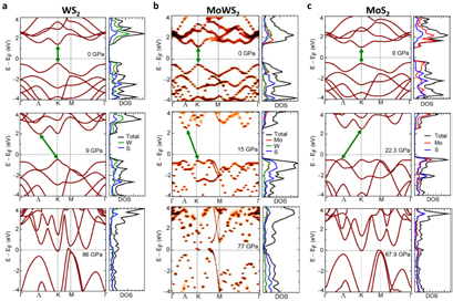
Figure 3. Band structure evolution of Mo(1−x)W(x)S2 under pressure. Band structures and DOS of monolayer (a) 1H–WS2, (b) 1H–MoWS2, and (c) 1H–MoS2 at ambient (top row), indirect transition (middle row), and metallization (bottom row) pressures. Green arrows indicate band gaps.
Download figure:
Standard image High-resolution imageThe difference in the D-to-I transition pressure and band gap opening rate regarding the composition can be attributed to the metal orbital contribution to the conduction band minima (CBM). The W contributions to the CBM/VBM follows the gradual change in W composition in nearly linear tendency [27]. Therefore, the pressure-dependence of band structures, which is closely related to the orbital contributions to the VBM and CBM, is also expected to show gradual change as a function of W composition. The band gaps of Mo(1−x)W(x)S2 monolayers with different W compositions as a function of pressure were calculated to confirm the composition dependency (figure S5). Band gaps at any given pressure, including metallization pressure, show linear relation to the W composition x. As pressure is applied, the CBM at the K point rises with the fastest rate in WS2, whereas the CB valley at the Λ point rises relatively slowly (upper panel of figure 3(a)). Also in the valence band, the VB valley at Λ point rises at a slow rate. The CBM(K) exceeds the CB valley at the Λ point and creates an indirect band gap with the VBM at the K point at low pressure (middle panel of figure 3(a)). Lower W composition results in slower rate of band gap opening as well as a delayed D-to-I transition. In the case of the MoWS2 alloy, W(d) states are located at the higher energy positions of the conduction bands than the Mo(d) states, and the hybridization between the Mo and W states is very limited. However, the Mo and W states are homogenously hybridized in the valence bands (figure 3(b)). As the pressure increases, the contribution from S (both W and S) becomes more dominant in the valence (conduction) bands. With increasing pressure, these orbitals move away from the Fermi level, resulting in an increase in the band gap. The rising rate of CB(K) is relatively slow compared to that of WS2, so it exceeds the CB(Λ) level at a higher pressure than WS2. Also, the VB valley at the Λ point rises with pressure but remains at lower energy at D-to-I transition pressures, forming an indirect band gap between the CBM(Λ) and the VBM(K) due to the fast-rising CB(K) (upper and middle panel of figure 3(b)). The increase in CB at the K-point is slowest in MoS2, so that the CB(K) remains the lowest energy valley at the D-to-I transition. Instead, the rapidly rising VB(Λ) exceeds the VB(K), and forms an indirect band gap at 22.3 GPa with the CBM at the K point (upper and middle panel of figure 3(c)) [1]. It is notable that despite seemingly similar D-to-I band transitions in Mo(1−x)W(x)S2 monolayers, the valleys forming the CBM and VBM could differ according to the composition. Therefore, the carrier behaviors such as effective mass could be different in Mo-rich systems and W-rich systems.
Calculated band gaps of WS2, MoWS2, and MoS2 with different thicknesses as a function of pressure are calculated as summarized in figure 4(a). Band gaps in bulk WS2, MoWS2, and MoS2 immediately decrease with applied pressure and metallize at pressures of 33 GPa, 27 GPa, and 23 GPa, respectively. In bilayers and monolayers, where sulfur–sulfur interaction is limited, applied pressure initially increases band gaps. Direct band gaps of monolayer WS2, MoWS2, and MoS2 increase until reaching indirect transition, and their maximum values at 21–24 GPa, and finally metallize at 86 GPa, 77 GPa, and 68 GPa, respectively. It is clear that the interaction between the layers induces charge concentration at chalcogen sites and therefore metallization is promoted [39]. The difference in the metallization pressure can be also understood in terms of their ionization potential, which controls the ability to transfer charge for Mo and W. In comparison to W, Mo has a lower ionization potential indicating that Mo can donate charges relatively easily and thereby facilitate the interaction between chalcogen atoms, which results in a S–M transition at a relatively lower pressure for MoS2 monolayer than in WS2. The same is true for bilayer and bulk MoS2/WS2 [56]. It is notable that extremely high pressure (>150 GPa) reportedly caused no structural transitions to bulk MoS2 other than Hc-to-Ha sliding at 29 GPa [48]. Moreover, bulk WS2 is reported to lack the sliding transitions and has more stable Hc phase [57]. Since the monolayers lack interlayer interactions and layer-sliding transitions, the pressure range discussed in this work is unlikely to induce structural transitions.

Figure 4. Band gap evolution of Mo(1−x)W(x)S2 with pressure. (a) Calculated band gap of WS2 (blue squares), MoWS2 (red triangles), and MoS2 (black circles) with varying layer number as a function of pressure. Direct band gaps are shown in open symbols, whereas indirect band gaps are shown in solid symbols. (b) Calculated conduction band minima (ECBM) and valence band maxima (EVMB) of monolayer 1H–Mo(1−x)W(x)S2 as a function of pressure. (c) Schematic of structure capable of applying pressure to selective regions of the monolayer. Pressure could be delivered by actuators, or transferred from external mechanical stress. (d) Schematics of Type-I, Type-II, and Type-III heterojunctions between strained and unstrained monolayer.
Download figure:
Standard image High-resolution image
Evolutions of individual CBMs, and valence band maxima (VBMs) of monolayer WS2, MoWS2, and MoS2 with respect to the vacuum level are summarized as a function of pressure in figure 4(b). For all monolayers, rapidly increasing CBMs and decreasing VBMs up to ~20 GPa lead to the band gap opening of the monolayers. VBMs show relatively similar pressure-dependent behavior regardless of metal composition, due to the similar contribution of W/Mo d-orbitals to the VBM. On the other hand, the different contribution of the metal d-orbitals to the CBM is responsible for the difference in the band structures. Considering the evolution of band gaps, it is conceivable that the hydrostatic compressive strains/pressures could be applied to monolayers to purposely modulate band edges. If a contact is formed between the strained/pressurized monolayer and unstrained monolayer or other smaller band gap 2D materials, the pressure-broadened band gap is expected to contain the other band gap and form a type I heterostructure (figure 4(d)). Interestingly, the VBMs increase after the pressure ~20 GPa, recovering initial values at pressures of 36 GPa, 31 GPa, and 28 GPa for WS2, MoWS2, and MoS2, respectively. The monolayers with pressure-elevated VBM and CBM above the ambient values are potentially suitable for forming a type II heterojunction with unstrained monolayers. The strained/pressurized monolayers are likely to extract holes and exhibit hole-dominant carrier behaviors. The DOS distributions marginally increase in the valence band, which will assist the p-type carrier behavior in the pressurized monolayer (figures 3(a)–(c) and Nayak et al [1]). With further pressure, VBMs continue to rise and even exceed the CBM levels at ambient conditions. This overtaking occurs at 77 GPa, 68 GPa, and 60 GPa for WS2, MoWS2, and MoS2, respectively. At such pressures, a contact with unstrained monolayer could form a type III heterojunction, where the charges from the pressurized VBM could tunnel directly to the unstrained CBM, which opens the possibility of tunneling devices.
In situ Raman spectroscopy was conducted for the monolayer WS2 and MoWS2 at high pressures to explore their pressure-dependent Raman shifts. In both WS2 and MoWS2 monolayers, in-plane (Eʹ) and out-of-plane (Aʹ) modes blue-shifted under applied pressure (figures 2(d) and S6–S8) [38, 58]. Higher pressure dependency of the Aʹ mode can be attributed to the faster normal compression and hampered lateral compression [1, 40, 43, 59, 60]. Also, it is notable that two Raman peaks denoted A† and A* were observed in the bilayer sample at pressures >15 GPa, but not in the monolayers, which confirms the interlayer disorder-related origin of the peaks (figure S9) [38]. Nevertheless, no obvious structural transition was observed in WS2 and MoWS2 up to ~30 GPa, suggesting the stable structure of monolayers even under extreme pressure. Raman spectra remained largely unchanged from the initial measurements and after quenching to ambient pressure (figure 2(d)), demonstrating that the pressure-induced electronic transition is a reversible process. Theoretical calculations were carried out to confirm the pressure evaluation of various phonon modes. The calculated phonon dispersion and density of states (DOS) are shown in figure S10, where the absence of negative phonon frequencies shows the dynamical stability of the structure. The pressure evolution of the Raman modes is in good agreement with the experimental results as shown in figure 2(d).
To demonstrate functional devices with modulated band offsets, structures capable of applying pressure or strain to a selective region are required, either to a particular layer in vertical heterostructures, or to a particular area of homogeneous monolayers (figure 4(c)). Such selective pressure could be actively provided by piezoelectric or electro/magnetostrictive actuators. Recent studies have suggested that TMD-based devices operating by piezoelectric gate barriers to be feasible, and could obtain a sub-60 mV/dec subthreshold swing (SS) [61, 62]. In energy harvesting devices or pressure/strain sensor applications, external mechanical stress could be passively delivered to a particular region of the monolayer [7, 63]. Moreover, composing lateral heterojunctions within a homogeneous monolayer could further overcome complications from stacking sequence or rotational alignment between the layers that are inevitable in vertical heterostructures [64, 65]. The pressure- and composition-engineered band structure could provide a wide range of band offsets and allow for the design of precise structures such as p-n junctions, quantum wells, superlattices, or tunneling structures. 2D-material-based optoelectronics such as transistors, light-emitting or detecting devices, and/or tunnel-FET could take advantage of the pressure-modulation technique.
3. Conclusion
In summary, pressure-dependent band structures of monolayer 1H–WS2 and 1H–Mo0.5W0.5S2 have been experimentally and theoretically explored to demonstrate the tunability of the band structure and band offset under compressive strain. The band gaps of monolayer Mo(1−x)W(x)S2 increased under pressure, where higher W composition contributed to faster band gap opening. With stable CBMs after the initial pressure increase, and significant rise of the VBMs, the strained monolayers are suggested to construct type I, type II, and type III heterojunctions with unstrained monolayers, according to the magnitude of applied pressure. Raman spectra of WS2 and MoWS2 monolayers experienced no noticeable structural transition or instability up to ~35 GPa, nor after recovering to ambient conditions, implying the pressure could provide reversible modulation of the polarity. The pressure modulation of carrier polarity in transition metal disulfides could allow for versatile engineering of opto-electronic device structures, such as logic devices, light-emitting devices, or photovoltaic devices.
4. Experimental section
4.1. Sample preparation
WS2 atomic layers were synthesized at Pennsylvania State University by atmospheric pressure chemical vapor deposition (CVD) method using WO3 (Alfa Aesar, 99.998%; 2 mg) and S (Alfa Aesar, 99.5%; 300 mg) powders as precursors (figure 1(a)). The sulfur powder and SiO2/Si target substrate were heated up to 250 °C and 800 °C, respectively. Argon (100 sccm) was used as a carrier gas during crystal growth. Detailed ramping parameters during the synthesis can be found in Lin et al [53]. After successful sample synthesis and recovery, the WS2 crystals and underlying substrate were cleaved and loaded into a diamond anvil cell (DAC).
Atomically thin MoWS2 flakes were mechanically exfoliated from bulk crystal (2D Semiconductors Inc.) onto a 90 nm SiO2/Si substrate, and annealed at high vacuum to remove tape residues. Suitable monolayer flakes were identified using optical microscopy, atomic force microscopy (AFM), and Raman/PL spectroscopy, and transferred either onto the Si substrate of thickness ~10 µm (University Wafers) that were placed on the diamond culet, or directly onto the culet using a dry transfer technique. Detailed dry transfer methods can be found in Kim et al [55]. Preparation and initial characterization of MoWS2 flakes were conducted at the University of Texas at Austin.
Screw-driven symmetric DACs with diamond culet size of 400 µm were used for the experiments. Re gaskets were indented to a thickness of ~40 µm and subsequently drilled with holes ranging from 190–230 µm in diameter to form sample chambers. Ne gas was used as a pressure medium, in order to minimize possible chemical reaction with or charge doping to the sample, while maintaining hydrostaticity up to the maximum pressure range of interest. The gas medium was loaded using the Gas Loading System in Mineral Physics Laboratory of the University of Texas at Austin. The pressure inside the sample chamber was determined by measuring the fluorescence of the ruby R1 line (figure S11) [66]. The pressure was slowly increased with 0.5–2 GPa increments.
4.2. Characterization and pressure experiments
The atomic ratio of the MoWS2 ternary alloy was determined using XPS with a Kratos x-ray photoelectron spectrometer—Axis Ultra DLD. CasaXPS software was used to fit peaks of the primary XPS peaks of the constituent elements, namely Mo 3d, W 4f and S 2p peaks. The S 2s peak was also fitted in order to exclude its overlap with the Mo 3d peak.
A Renishaw inVia micro-Raman system coupled with a 532 nm laser, and a WiTEC Alpha 300 micro-Raman system coupled with a 488 nm laser were used for the initial characterization as well as in situ pressure experiments of 1H–WS2 and 1H–MoWS2, respectively. The spectral resolution in Raman measurement of WS2 was ~1.2 cm−1 (2400 line mm−1 grating). A laser power of ~20 mW was used, while collection time was varied depending on the spectral quality. The spectral resolution in Raman measurements of MoWS2 was ~0.9 cm−1. A maximum laser power of ~2 mW was used for the Raman measurements. However, the power controller of the laser can only be manually adjusted, so that the precision over laser power is limited. For all cases, the laser was focused within a ~1 µm spot size. Lorentzian curve fitting was used in the spectral analysis of Raman spectra. Note that the MoWS2 flake for in situ Raman experiments was transferred directly onto the diamond culet because the Si substrate used in PL experiments was unstable at >13 GPa due to the structural phase transition of Si.
4.3. First-principle theoretical calculations
To generate the ideal random alloy of monolayer Mo0.5W0.5S2, the special quasi-random structures generation (SQS) method [67, 68] was used with three different supercell sizes of 4 × 4 × 1, 6 × 6 × 1, and 8 × 8 × 1. Since the band gap values are identical regardless of the supercell size, 6 × 6 × 1 cell was used for monolayer, and 4 × 4 × 1 for bulk and bilayer, to minimize the computational cost. The first-principles density functional theory, as implemented in the VASP package, was used for structural relaxation and electronic structure calculations [69, 70]. The projector augmented wave method and generalized gradient approximation within the framework of Perdew–Burke–Ernzerhof was adopted for the electron exchange and correlation [71]. The kinetic energy cutoff for the plane wave basis is set to 500 eV. The Γ-centered 7 × 7 × 1 k-point mesh is used for the Brillouin zone integration, with an energy convergence criterion of 10−4. A 15 Å vacuum was applied along the c direction for modeling the isolated layers. All structures were fully relaxed until the force on each atom is less than 0.005 eV Å−1. The method to apply hydrostatic pressure on monolayer is presented in detail in the previous works [1, 41]. In order to obtain effective band structures, the eigenvalues of the large supercells were unfolded into a primitive cell by a spectral function (SF) of continuous variable energy [72, 73]. The phonon spectra of MoWS2 was calculated using the finite displacement method by using PHONOPY code [74, 75]. The force constant matrix was calculated on 2 × 2 × 1 supercell along with a k-point grid of 3 × 3 × 1 by using VASP code. To obtain accurate phonon frequencies, a high-energy cutoff of 600 eV and strict energy convergence criterion of 10−7 eV were used. Non-resonant first-order Raman calculations under pressure for MoWS2 alloys were performed within VASP using the method proposed by Fonari et al [76].
Acknowledgement
This work is supported in part by the Defense Threat Reduction Agency (DTRA) Young Investigator Program (DA). SF, ZL, and MT acknowledge the financial support from the U.S. Army Research Office under MURI grant (W911NF-11-1-0362) and the National Science Foundation (2DARE-EFRI-1433311). Research at Indian Institute of Science was supported by DST Nanomission. JFL acknowledges support from Center for High Pressure Science and Technology Advanced Research (HPSTAR). The authors acknowledge Super Computing Education and Research Center (SERC) and Materials Research Center (MRC), at Indian Institute of Science Bangalore for providing required computational facilities. RA acknowledges the financial support from INSPIRE fellowship, AORC. We thank Dr Hugo Celio, Dr Anupam Roy, and Hema C P Movva for their contribution to sample preparation and analysis of MoWS2. Authors also thank prof. Yaguo Wang, Dr Ke Chen, and Richard Roberts for valuable discussions and editing that enriched this study.