
Abstract
Thermoelectric properties of materials are typically evaluated using the figure of merit, ZT, which relies on both the electrical and thermal properties of the materials. Although graphene has a high thermoelectric power factor, its overall ZT value is quite low as it possesses extremely high thermal conductivity. Phonons are the main heat carrier in graphene, and therefore propagation of heat in the material may be modulated by introducing defects into the structure, resulting in reduced thermal conductivity. In this study, we investigate the effect of graphene defect density on the thermoelectric performance of graphene. The defects introduced into graphene by oxygen plasma treatment reduce its Seebeck coefficient as well as its electrical conductivity; as a result, the thermoelectric power factor declines with increasing defect density. However, at higher defect densities, the reduction in thermal conductivity dominates over the reduction in electrical conductivity and, consequently, graphene treated in this way is observed to possess ZT values of up to three times that of pristine graphene. Therefore, it may be concluded that introducing controlled amount of defects into graphene is an effective way of reducing its thermal conductivity, thereby enhancing the performance of graphene-based thermoelectric devices.
Export citation and abstract BibTeX RIS

Original content from this work may be used under the terms of the Creative Commons Attribution 3.0 licence. Any further distribution of this work must maintain attribution to the author(s) and the title of the work, journal citation and DOI.
Introduction
Understanding heat conduction in materials is important for thermal management of electronic devices and energy recycling; for example, in an electronic device, a heat exchanger with high thermal conductivity is necessary to dissipate the excess heat generated by the electronic components. On the other hand, thermal energy recycling can be achieved through thermoelectric conversion, which requires materials with a high power factor (PF = S2σ, where S and σ are the Seebeck coefficient and electrical conductivity, respectively) and low thermal conductivity, κ; such materials possess high values of ZT, the standard figure of merit for thermoelectric materials (ZT = (S2σ/κ)T, T being the absolute temperature), and therefore display high thermoelectric conversion efficiencies. In essence, control of the thermal conductivity is crucial in the effective application of these materials. From this viewpoint, graphene has been considered as a candidate for thermal management due to its outstanding electrical, mechanical, and thermal properties, such as extremely high carrier mobility [1–3], flexibility [4, 5], and thermal conductivity [6]. In particular, graphene has been earmarked as a suitable material for heat dissipation due to its extremely high thermal conductivity [7]. In terms of thermoelectric conversion, graphene exhibits high electrical conductivity and a Seebeck coefficient of ~100 µV K−1 at room temperature [8, 9], resulting in a higher overall PF than other semiconductors and metals. However, the overall ZT value of graphene is normally quite low, owing to its extremely high thermal conductivity; as such, reducing the thermal conductivity of graphene—importantly, without significantly reducing the electrical properties of the material—is imperative for increasing its ZT value. Since the main heat carrier in graphene is phonon, the thermal conductivity can be reduced by introducing carbon isotopes [10–12], structural defects [12–15], domain boundaries [16, 17], or wrinkles [18, 19] into the structure, or by functionalization [20]. While introduction of domain boundaries and wrinkles decreases experimentally the thermal conductivity of graphene by less than 50%, random substitution of half of the carbon atoms with carbon isotopes, has been observed to yield a 50% reduction in thermal conductivity [10]. Further reductions in thermal conductivity may be achieved by forming a well-defined isotopic heterojunction between a 12C graphene film and a 13C graphene film, owing to the phonon frequency mismatch between the two sheets [11]. Another significant advantage of using isotopically substituted graphene this changes neither the electrical properties nor the PF of graphene [21]. However, practical application of graphene in thermoelectric devices requires even greater reductions in thermal conductivity. A promising route to achieve these was recently demonstrated by Zhao et al, who showed that the thermal conductivity of graphene can be reduced by more than 90% by introducing structural defects by oxygen plasma treatment [22]. Although this modification alters the electrical properties of the graphene films, the effect of the presence of defects on thermoelectric performance has not been investigated to this point, nor have these films been evaluated for application. It should also be mentioned that the controlling the amount and type of defects even increases the electrical conductivity of graphene [23]. Therefore, in this study, we use oxygen plasma treatment to induce defects in graphene and investigate the subsequent changes in its thermal conductivity and thermoelectric properties, with the ultimate goal of enhancing the material's thermoelectric performance.
Experimental section
Graphene synthesis and device fabrication
Graphene was synthesized by low-pressure chemical vapor deposition (CVD), using CH4 as a carbon source and Cu foils as catalyst. The grown graphene was monolayer with the domain size of 100–700 µm (300 µm on average), indicating that the graphene used in this study was single-domain. Details of growth conditions are described elsewhere [21]. Subsequently, graphene was transferred onto Si substrates with a thermally oxidized 500 nm thick SiO2 layer, on which a Pt micro-heater and Pt electrodes were deposited in advance in order to measure the electrical and thermoelectric properties. For thermal conductivity measurements, Au-coated silicon nitride (Si3N4) substrates with 2.5 µm diameter holes were used instead of SiO2/Si. For electrical and thermoelectric measurements, the graphene films were patterned by oxygen plasma, yielding microchannels with width and length of 5 µm and 10 µm, respectively.
Electrical and thermoelectric measurements
For measurement of the electrical and thermoelectric properties, the Pt micro-heater and four Pt electrodes were deposited by e-beam on the SiO2/Si substrate. A temperature gradient was generated along the graphene channel by the electric current running through the micro-heater. The inner electrodes serve both as thermometers and as a voltmeter between the two ends of the graphene sample. The temperature difference (ΔT) was evaluated by measuring the temperature coefficient of the inner electrodes using four-terminal method, and the Seebeck coefficient was estimated from the thermovoltage (ΔV) and the temperature difference (ΔT) between the inner electrodes. Prior to measurement, the graphene samples were annealed in vacuum (~10−3 Pa) at 150 °C for 4 h. All the measurements were performed in vacuum at room temperature.
Thermal conductivity measurement
The thermal conductivity of graphene was measured by Raman spectroscopy. Detail of the thermal conductivity measurement is described in the supporting information (stacks.iop.org/TDM/4/025019/mmedia). Briefly, the center of the graphene film was suspended over a hole and irradiated using a laser of wavelength 532 nm. The laser also generates heat at the center of the graphene film that dissipates towards the edge of the sample; as a result, the graphene temperature at the point of irradiation depends on the distance between the center and the edge. The thermal conductivity was estimated by  , where R is the radius of the hole, r0 is the laser radius, Q is the absorbed laser power, t is the thickness of graphene, and ΔT is the temperature difference between the center and the edge of the graphene [24, 25]. In this study, 1.25 µm and 0.26 µm were used for R and r0, respectively. For monolayer graphene, t is 0.335 nm. The temperature at the center of the film was estimated from Raman 2D peak shifts, after the temperature coefficient of the same graphene film was initially obtained by heating the substrate.
Results and discussion
Oxygen plasma treatment was used to introduce defects into graphene, with control of the generated defect density achieved by changing the plasma intensity and the treatment time [26]. Specifically, the RF plasma was generated by 50 W for 2–12 s for supported graphene samples and 35 W for 1 s for suspended samples. Oxygen partial pressure was set to be 40 Pa. Figure 1(a) shows the evolution of the Raman spectra of graphene films with different defect densities. Generally, the intensity ratio between Raman D (~1350 cm−1) and G (~1580 cm−1) bands, D/G, was used to estimate the defect density. D band intensity reflects the amount of defects, indicating that D/G increases with increasing the defect density. The Raman spectrum of as-prepared graphene (D/G = 0.04) indicates that the film consists of a monolayer with few defects. Figure 1(b) shows a 2D intensity map of the D band intensity that depicts that the defects in graphene were uniformly distributed after oxygen plasma treatment. Figure 1(c) shows the observed changes in D/G and 2D/G ratios as the number of plasma treatment cycles increases from 0 to 3. D/G was increased up to 2.47, while 2D/G ratio was reduced from 2.18 to 0.77 with increasing defect density. The defect density is often referred by LD that is the average distance between defects. LD is given by [27, 28]
where CA is a weighting coefficient, rS is the radius of the structurally disordered area, and rA is the radius of the area where the D band scattering takes place, although the hexagonal lattice structure is preserved. In this study, 4.2, 3.1 nm, and 1 nm were used for CA, rA, and rS, respectively [27, 28]. In this series of graphene films, the D/G ratios of approximately 0.04, 0.54, 1.74, and 2.47 correspond to LD values of 49.9 nm, 13.9 nm, 6.9 nm, and 5.2 nm, respectively.

Figure 1. (a) Raman spectra of the same monolayer graphene with 4 different defect densities introduced by oxygen plasma treatment. (b) D band intensity mapping of the graphene device. The white dashed lines mark the boundaries between graphene and the electrodes. (c) Change in D/G and 2D/G with increasing plasma treatment cycles, where each exposure lasted for ~0.5 s.
Download figure:
Standard image High-resolution imageElectrical conductivity and the field-effect mobility of graphene field-effect transistors (FETs) were measured by obtaining their transfer characteristics, using four-terminal device structures as depicted in figure 2(a). Figure 2(b) shows the electrical conductivity of graphene films with different defect densities as a function of back gate voltage, VG. The conductivity and field-effect mobility were both observed to decline in films with increased defect density; the field-effect mobility of as-prepared graphene is 2840 cm2 V−1 s−1, whereas plasma-treated graphene with a D/G = 2.61 yielded up to 64% and 90% reductions in electrical conductivity and field-effect mobility, respectively. This may be explained by the scattering of carriers at defect sites that increases with the increasing defect population. In addition, the Dirac point was observed to shift from −20 V to 177 V on oxygen plasma treatment; this is attributed to the modification of the carbon networks in graphene with functional groups which, in turn, introduce charged impurities into the material as dopants. Figure 2(c) plots the change in graphene Seebeck coefficient with the defect density. The Seebeck coefficient can be easily changed by tuning the gate voltage ΔVG (=VG − VD; VD is the voltage at the Dirac point). The sign of the Seebeck coefficient was seen to change from positive to negative across the Dirac point, depending on the carrier types. At the Dirac point, the Seebeck coefficient becomes zero because holes and electrons in graphene are equivalent. As the defect density increases, the peak Seebeck coefficient was observed to decrease [29]; in addition, the increased density of defects shifts the ΔVG at which the Seebeck coefficient reaches its maximum further from the Dirac point. This observed decrease in the Seebeck coefficient and the peak position shifts are also thought to arise from the increase in charged impurities in the graphene channel [30]. Given that the PF depends both on the Seebeck coefficient and on electrical conductivity, the decrease in both values on introduction of defects into graphene indicates that the overall PF will also decrease: this is presented in figure 2(d) that plots the ratio PF/PF0, i.e. the ratio between the measured PF and the PF of pristine graphene (PF0), with respect to D/G. At the highest defect density, where D/G = 2.61, PF/PF0 was observed to decrease down to 16%. The inset of figure 2(d) plots PF against ΔVG at the hole side, showing that for films with different defect density, the PF changes on tuning the gate voltage, similar to the trends observed for the Seebeck coefficient in figure 2(c); in addition, PF reaches zero at the Dirac point at which the Seebeck coefficient is also 0.
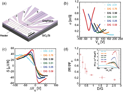
Figure 2. (a) Optical micrograph of the device used for thermoelectric measurements showing the position of the micro-heater and the four electrodes (labeled from 1 to 4). (b) Typical electrical conductivity of graphene films with different defect populations as a function of VG. (c) Change in Seebeck coefficient on tuning the gate voltage, ΔVG for the graphene films at the different defect density. (d) Change in PF (normalized with respect to the PF value for as-deposited graphene, PF0) values at different defect populations, D/G. Inset shows PF as a function of ΔVG for different defect densities.
Download figure:
Standard image High-resolution imageThe direction of change in the ZT value of graphene on introducing defects depends on the degree to which thermal conductivity is reduced in comparison to the electrical conductivity. To investigate the defect-induced changes in thermal conductivity of graphene, we fabricated suspended graphene films on Au-coated Si3N4 substrates in order to measure the thermal conductivity by Raman spectroscopy, as outlined in the experimental section: this is illustrated in figure 3(a). Both scanning electron microscopy (SEM) and Raman spectroscopy were used to verify that the graphene films were correctly suspended over the holes: figure 3(b) shows both holes covered with the graphene film and those uncovered, and it was found that this could be simply determined visually by the image contrast. In addition, the graphene was found to fully cover the holes and exhibited no signs of tears or wrinkles. Of 14 prepared samples, 6 were selected to measure the thermal conductivity. Figure 3(c) shows Raman 2D band intensity mapping from the same area as that of the SEM image shown in figure 3(b). The 2D peak intensity of the suspended graphene is more intense than that of the graphene supported on the substrate, allowing for simple visual distinction between the two regions. Figure 3(d) depicts the change in the thermal conductivity with increasing the defect density. The thermal conductivity of as-prepared graphene grown by CVD was measured to be 3367.6 ± 485.0 W m−1 K−1, which corresponds to the values previously reported [10, 11, 22, 24, 25]. As phonons act as the main heat carrier in graphene, the thermal conductivity can be dramatically reduced by introducing structural defects. In our study, the thermal conductivity of the suspended graphene film with D/G = 2.42 (highest defect density) was found to be just 5.6% of that of the as-prepared graphene (D/G = 0.04). Note that the thermal conductivity of graphene supported on the SiO2 substrate was also measured for comparison according to the recent publications [24, 31]. Details of the measurement and results are shown in the Supporting Information. The thermal conductivities of as-prepared and defective graphene (D/G = 2.51) supported on the substrate were 543 W m−1 K−1 and 36 W m−1 K−1, respectively. Although these values are smaller than those of as-prepared and defective graphene suspended over a hole, as expected due to damping of ZA phonons [32], it can be concluded that oxygen plasma treatment is an effective way to drastically reduce the thermal conductivity of both suspended and supported graphene samples.
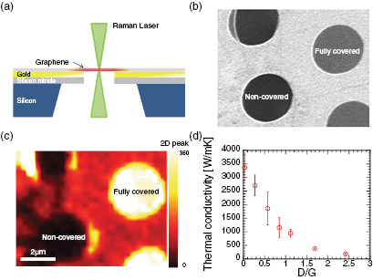
Figure 3. (a) Schematic illustration depicting thermal measurement of suspended graphene films by Raman spectroscopy. (b) SEM and (c) Raman 2D band intensity mapping of graphene situated over the holes in the substrate. Fully covered and non-covered holes with graphene can be identified by the contrast in SEM and Raman spectroscopy. (d) Defect density dependence of the thermal conductivity of suspended graphene.
Download figure:
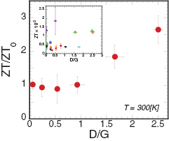
Standard image High-resolution imageFinally, we evaluate the defect-induced change in the graphene thermoelectric figure of merit, ZT = (PF/κ)T. In this study, each measurement was performed at room temperature. From the results in figures 2(d) and 3(d), we calculated the ratio ZT/ZT0 for each graphene film, where ZT0 is the ZT of pristine graphene, as shown in figure 4. Absolute ZT values from all the samples are present in figure 4 inset. At lower defect density (for films with D/G up to ~1.0), ZT remains almost constant irrespective of the defect density because the decreases in both PF and κ are comparable in this range. The absolute ZT value of pristine graphene is 0.55 × 10⁻³ at room temperature. For the film with the highest defect density (D/G ~2.61), however, the ZT was found to increases markedly. In this range, the defect-induced reduction in thermal conductivity becomes the dominant factor over the corresponding decrease in power factor, leading to an approximately threefold increase in ZT value. It is expected that the ZT value would begin to decrease as the defect density further increases. This may occur as the electrical conductivity diminishes more drastically, owing to disruption of the graphene structure. Therefore, in order to increase the thermoelectric performance of graphene devices, the defect density must be carefully controlled. From these results, we have shown that introducing defects into graphene is an effective strategy for modulating the material's thermoelectric properties, thereby making it more suitable for incorporation into thermoelectric devices. In addition, graphene maintains a substantial degree of sp2 binding networks even after oxygen plasma treatment, meaning that the thermal conductivity could be further reduced by structural modifications such as introducing carbon isotopes and 5–8 defects. Carbon isotopes reduce the thermal conductivity without affecting the electrical properties [21], whereas 5–8 defects can increase the electrical conductivity and reduce the thermal conductivity [23]. Therefore, a combined approach of defect introduction and isotopic substitution may further improve graphene ZT values, thereby making them even better suited to thermoelectric applications.
Figure 4. Normalized ZT values, ZT/ZT0, with respect to D/G at room temperature. Inset shows the actual ZT values from all the samples examined in this study.
Download figure:
Standard image High-resolution image
Conclusion
We investigated the effect of oxygen plasma-induced defects in graphene on thermoelectric performance by evaluating the thermoelectric figure of merit, ZT. The electrical conductivity, Seebeck coefficient, and thermal conductivity were measured for graphene with defects introduced by oxygen plasma treatment. At lower defect densities, ZT remained unchanged, although both PF and thermal conductivity were reduced by introducing defects. At higher defect density, ZT was observed to increase to a value three times higher than that of pristine graphene. Although both the electrical conductivity and Seebeck coefficient were found to decrease with increasing defect populations, it was possible to control the defect populations such that the reduction in thermal conductivity was dominant. As a result, we conclude that it is possible to enhance the ZT of graphene through defect formation, which is a new route for enhancing the thermoelectric performance of graphene devices.
Acknowledgments
This work was partially supported by a grant from The Murata Science Foundation, MEXT KAKENHI Grant Number 15H05869, and JSPS KAKENHI Grant Numbers 16H04283 and 15J12244.