

Abstract
Single-photon sources are important building blocks for quantum information technology. Emitters based on solid-state systems provide a viable route to integration in photonic devices. Here, we report on single-photon emitters in the layered semiconductor GaSe. We identify the exciton and biexciton transition of the quantum emitters with power-dependent photoluminescence and photon statistics measurements. We find evidence that the localization of the excitons is related to deformations of the GaSe crystal, caused by nanoscale selenium inclusions, which are incorporated in the crystal. These deformations give rise to local strain fields, which induce confinement potentials for the excitons. This mechanism lights the way for the controlled positioning of single-photon emitters in GaSe on the nanoscale.
Export citation and abstract BibTeX RIS
Since the discovery of graphene, 2D materials have gained widespread attention because of their extraordinary physical properties. Transition metal dichalcogenides (TMDCs), such as MoS2, WS2, MoSe2, WSe2, and MoTe2 represent a unique class of semiconductors, because of their transition from an indirect to a direct band gap material when thinned down to a monolayer [1–3]. Recently, single-photon emitters [4], have been found in monolayers of tungsten diselenide (WSe2) [5–9]. This discovery has stimulated the search for single-photon sources in other 2D materials. Single-photon emitters have been identified in WS2 [10], and narrow emission lines of localized centers have been found in MoSe2 [11]. A different class of single-photon emitters has been detected in hexagonal boron nitride (hBN) [12]. They have been associated with defects in the host crystal, similar to color centers in diamond [13]. In general, the localization of excitons in semiconductors can be achieved by confining them in quantum dots [14], by binding them to impurities [15], or by strain-induced potential traps [16–20]. However, in contrast to conventional semiconductors such as silicon or GaAs, the extraordinary mechanical properties of 2D materials allows for applying strain of a few percent and strong nanoscale bending. Indeed, the origin of the quantum emission in atomically thin WSe2 has been related to strain-induced local confinement potentials, which trap free excitons [5, 21, 22]. Here, we report on the discovery of single-photon emitters in GaSe. We find that the emitters occur due to local deformations of the GaSe crystal, which are caused by nanoscale Se clusters. The strain induced in the GaSe crystal leads to local confinement potentials, which trap excitons.
Bulk gallium selenide is a well-known material for non-linear optics, since it has a high nonlinear coefficient and damage threshold [23]. Efficient second-harmonic [24] and THz generation [25] has been demonstrated. Few-layer or atomically thin GaSe is promising for electro-optical devices, such as transistors [26] and photodetectors [27]. Gallium selenide belongs to the group of gallium chalcogenides, which crystallize in a layered structure with strong covalent (partly ionic) intra-layer bonds and weak, predominant van der Waals inter-layer bonding. A 'monolayer' of GaSe consists of four atomic layers with two layers of Ga atoms enclosed by two layers of chalcogen atoms (Se–Ga–Ga–Se). Our GaSe single crystals are grown by high pressure vertical zone melting in graphite crucibles in Ar atmosphere [28]. GaSe crystals with a thickness of a few tens of nanometers and lateral extensions of typically tens of micrometers are fabricated by mechanical exfoliation on a SiO2 (290 nm)/Si substrate. Subsequently, a Si3N4 layer of 10 nm is deposited by plasma-enhanced chemical vapor deposition on top of the sample to protect the GaSe flakes from ambient oxygen and water [29].
GaSe crystals on SiO2/Si substrate are identified with optical reflection and atomic force microscopy (figures 1(a) and (b)). The photoluminescence (PL) emission is measured with a homebuilt confocal laser scanning microscope at cryogenic (T = 10 K) and at room temperature [5]. Interestingly, we find various locations on the GaSe crystal with a strongly increased PL emission (figures 1(c) and (d)), while the surrounding flake area exhibits only very weak emission. The lateral size of these localized emission centers is governed by the spatial resolution of the experimental setup and amounts to 490 nm full width at half maximum (FWHM). The observed light emission is stable and does not show any blinking or spectral wandering. It exhibits either a single prominent line or a double peak in the range 1.7–2.0 eV. A spectrum of one emission center with a double peak structure recorded at low temperature is displayed in figure 1(e) (red curve). The two prominent emission lines are centered at 1.881 and 1.874 eV (ΔE = 7 meV) with a FWHM line width of 3.7 meV and 5.2 meV, respectively. The relative amplitude of the two maxima depends on the excitation power. At low excitation power only the energetically higher emission is visible, while with increasing power the other one brightens faster (see discussion below). The energetic separation of the two lines varies from center to center (ΔE = 2.6–8 meV), and for a significant number of emitters only one line is visible (see supporting information, figures S1 and S2). In addition, a weak emission at 2.03 eV is discernible. We assign this line to the bound exciton. The free exciton in GaSe has been reported previously at higher energy (2.11 eV) [30, 31]. Free excitons can bind to structural defects or impurities, so that at low temperatures their emission is suppressed in favor of the bound excitons [31–34].

Figure 1. (a) Optical reflection and (b) atomic force micrograph of a 36 nm thick GaSe crystal covered with 10 nm Si3N4. (c) and (d) The photoluminescence images show several diffraction-limited localized light sources in the GaSe crystal, recorded at a temperature of (c) T = 295 K and (d) T = 10 K. (e) Typical photoluminescence spectra of the emitters at a temperature of T = 295 K and 10 K.
Download figure:
Standard image High-resolution imageRemarkably, most of the bright emission centers are still observable at room temperature (T = 295 K). For the emitter shown in figure 1(e), the PL maximum shifts down to 1.74 eV and broadens to 100 meV (figure 1(e), black curve). The PL of other emitters is centered between 1.70 and 1.82 eV and has a similar line width (see supporting information, figure S3). At room temperature, the signature of the free or bound exciton of bulk GaSe around 2 eV is very weak and only visible at a high excitation power (60 kW cm−2).
To gain further insight into the properties of the two emission maxima of a single emission center we perform power-dependent PL measurements (figure 2(a)). As mentioned before, at low excitation powers of several tens of W cm−2 typically only one emission line is visible. We believe that the emission stems from a localized exciton (LX). With increasing excitation power, a second line (LXX) appears on the low energy side for some emitters. The new line rises faster with excitation power compared to the initial one (figure 2(b)). Interestingly, the intensity I of the LX line has a sub-linear power dependence according to I ~ P0.6. This behavior is similar to the bound exciton (X) at 2.03 eV, which has a slope of 0.7 (figure 2(b)). This sub-linear increase has been reported previously for bound excitons in 2D semiconductors [35] and GaSe [36] as well as for multiple quantum wells [37], while free excitons exhibit a linear increase with the power. The low energy emission LXX at 1.957 eV increases quadratically compared to the localized exciton LX ( ), which is typical for biexcitons [38]. Therefore, we believe that the second line LXX represents the biexciton transition of the localized emission center.
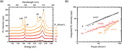
Figure 2. Power-dependent photoluminescence (PL) measurement. (a) PL spectra of a single emitter with two emission lines LX and LXX, and the bound exciton of GaSe (X) for different excitation powers. The additional lines X1, X2, and X3 appearing at higher excitation powers might be related to the same or a second emitter. (b) Integrated intensity of X, LX, and LXX depending on the excitation power. In the double-logarithmic plot the slope of the LXX line is twice the slope of the LX line.
Download figure:
Standard image High-resolution imageIn order to investigate the nature of the localized emitters we measure the photon statistics using a Hanbury Brown and Twiss setup (HBT). A grating spectrometer blocks the PL except for the energy range of the narrow band exciton emission (LX) at 1.881 ± 0.002 eV (high energy line in figure 1(e)). The second-order correlation function g(2)(τ) is shown in figure 3(a). The deep minimum at zero time delay g(2)(τ = 0) = 0.33 proves that the localized light source is a single-photon source. The rise time of the second-order correlation function g(2)(τ) is determined by the excitation rate and luminescence decay time and amounts to 7 ns for this emitter. Time-resolved PL measurements of other emitters yield decay times between 5 and 22 ns (see supporting information, figure S4). Interestingly, we find that emitters without a second emission line appearing at higher excitation power exhibit no or only a small antibunching dip (g(2)(τ = 0) is significantly larger than 0.5), which are therefore not single-photon emitters.
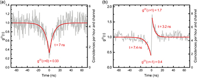
Figure 3. (a) Photon statistics measurement of the localized light source of figure 1(e), measured in the energy range 1.881 ± 0.002 eV at a temperature of T = 10 K. The minimum of the recorded second-order correlation function g(2)(τ = 0) is 0.33, which proves that the localized emitter is a single-photon source. (b) Cross-correlation measurement of LX and LXX from the single emitter shown in figure 2.
Download figure:
Standard image High-resolution imageTo prove that for an emission center with a double peak structure the two emission lines originate from the same emitter a cross-correlation measurement is performed (figure 3(b)). The signal of the high and the low energy line (LX and LXX) is dispersed in a spectrometer and routed to separate single-photon counters. The counter detecting the LXX emission triggers the start of the time measurement, while the counter for LX stops it. Positive times correspond to an event where first a LXX photon is detected, followed by the detection of a LX photon. The strong bunching signal for small positive times indicates the presence of the biexciton. After the decay of the biexciton there is an enhanced probability of the decay of the exciton (biexciton–exciton cascade [39]). Therefore, the two emission lines at 1.965 and 1.957 eV in figure 2 are due to the localized exciton and biexciton, respectively, with the binding energy of the biexciton given by the energy difference between the two emission lines. In general, the wider the potential well, the lower is the binding energy of the biexciton [40]. If the potential is too wide, the exciton and the biexciton cannot be spectrally resolved, in case the biexciton binding energy is smaller than the line width. This seems to be the case for the majority of the emission centers, where only one emission line appears even at higher excitation powers. Consequently, these are also emitters which exhibit no antibunching. In contrast, all emission centers proven to be single-photon sources exhibit a separate biexciton line at higher powers and therefore should reside in narrower potential wells. The spatial extent of the confinement potential can be estimated using a simple model for the binding energy of an biexciton in a spherical potential well [41]. The binding energy is given by  , where M is the translational mass of the exciton given by the sum of the effective masses of electron (
 ) and hole (
 ) [42] and R is the effective radius of the potential well.
  is the biexciton binding energy in bulk GaSe, which has been reported to be ~2 meV [43]. The measured biexciton binding energies between 2.6 and 8 meV yield an effective radius between 22 and 7 nm, corresponding to a diameter (width) of the potential well of 44 and 14 nm, respectively.
At room temperature, the photoluminescence of some localized centers is still visible (figures 1(c) and (e)). However, we do not observe significant antibunching due to an increased background from the surroundings of the emitter and a substantial overlap of biexciton and exciton lines due to their broadening.
We now turn to the origin of the single-photon emitters. By comparing the light emission in the photoluminescence maps (figure 4(a)) with the topography of the sample obtained by an atomic force microscope (AFM) measurement (figure 4(b)) of the GaSe flake, we find that the localized light sources are located at position of small elevated islands on the GaSe crystal. They have typical lateral extensions of 200–400 nm and heights of 3–10 nm. The islands have a smooth AFM line profile, implying a bulging of the GaSe surface (figure 4(c)) caused by a nanoobject underneath. This is in contrast to the small GaSe piece on top of the large flake (bottom left in figure 4(b)), which has a steep edge given by the spatial resolution of the AFM. It has been shown, that GaSe crystals may contain Se inclusions with sizes of 60–300 nm [44], which could lead to a locally modified and strained lattice. To prove that these inclusions are also present in our sample, the Si3N4 capping layer is mechanically removed by scratching with a stainless-steel tweezer on a different part of the sample. We investigate this region with a scanning electron microscope (SEM) equipped with an energy-dispersive x-ray spectroscopy (EDX) detector. Indeed, we find small nanoparticles with diameters of up to 300 nm. At position of the particles we detect a significantly enhanced EDX signal from selenium atoms as compared to the GaSe crystal (see supporting information, figure S5), indicating that these nanoobjects are selenium clusters. The Se clusters are most probably formed during crystal growth [45]. Once they appear, they force the surrounding layers of GaSe to bend, which leads to islands with a smooth profile on top of the GaSe crystal as illustrated in figure 4(d). In a simple model, we approximate the bending of the consecutive GaSe layers around a small Se cluster with a Gaussian, so that the profile of the topmost GaSe layer closely resembles the measured AFM profile of the island in figure 4(c). The color of the GaSe layers in figure 4(d) indicates their curvature  , i.e. the inverse bending radius R of a single layer with the height profile y(x). GaSe layers close to the Se cluster experience strong bending on the nanoscale, while more distant layers undergo a weaker bending. The curvature changes bond angles and bond lengths, which leads to bending-induced local strain [46–48]. In this way, a strain-induced localized potential well is formed near the Se cluster. In our simple model, the width of the potential well has an approximate size of the radius of the Se cluster, which is a few nm (roughly the height of the islands) and is on the order of the Bohr radius of excitons in GaSe [44]. This spatial extent agrees well with the result of the model for the biexciton binding energy presented above.
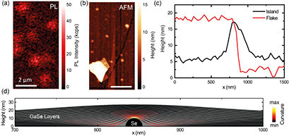
Figure 4. Light emission and topography of a GaSe crystal. (a) Photoluminescence map with several bright emission centers, which occur at elevated islands shown in the AFM image (b). (c) AFM line profiles of the islands (black line) are smooth compared to a second GaSe flake (red line) laying on top of the large one in the lower left corner in (b). (d) GaSe layers bent around a 20 nm Se cluster (black half sphere). The color of the GaSe layer indicates its curvature, which leads to local strain.
Download figure:
Standard image High-resolution imageWe not only find sharp emission lines at the small islands, but also when two different GaSe flakes are lying on top of each other. At the intersection, where the upper flake is bent due to the underlying one, narrow emission lines appear. Importantly, the single-photon emitters do not occur, where particles are lying on top of the GaSe surface (with sharp edges in the AFM line scan). Thus, the emission centers only occur when the GaSe flake is bent.
Further indication for the role of strain in the creation of single-photon emitters is found with photoluminescence excitation spectroscopy (PLE). The PLE spectrum of the emitter of figure 1(e) is presented in figure 5. It exhibits a broad maximum centered at 2.09 eV before it drops to a local minimum at 2.10 eV. The PLE spectrum resembles the absorption spectrum of the free exciton in bulk GaSe [44], providing evidence that the single-photon emitter is excited via the free exciton. The PLE spectrum is similar for all localized emission centers, although at the same time the PL emission of the individual emitters varies in a wide spectral range (1.7–2.0 eV). A closer look at the broad PLE maximum at 2.09 eV reveals that it is split into two resonances with a separation of 8 meV. For other emitters, the PLE maximum at the excitonic transition is split by up to 20 meV. The center of the double peak remains at a constant energy while both absorption lines are shifted symmetrically (see supporting information, figure S6). Recently, it was demonstrated that a splitting of the excitonic absorption can be caused by hydrogen intercalation of GaSe. The intercalation deforms the lattice leading to a quasi-2D localized excitonic state and a splitting in the absorption spectrum [44]. Therefore, this observation is another indication that the deformation of the GaSe lattice plays an important role for the formation of the single-photon emitters. However, for our GaSe multilayers we cannot exclude that defects in the crystal lattice or impurities are also involved in the formation of the single-photon emitters.

Figure 5. PLE spectroscopy of the emitter of figure 1(e), revealing a broad absorption maximum at 2.09 eV due to the free neutral exciton in GaSe.
Download figure:
Standard image High-resolution image
In summary, we have found single-photon emitters in GaSe, which are identified with photon correlation measurements. The observation of the exciton–biexciton cascade renders these emitters also interesting candidates for entangled photon sources [49]. Atomic force microscope and energy-dispersive x-ray spectroscopy measurements indicate that the localization of the excitons is related to deformations of the GaSe crystal, caused by incorporated nanoscale selenium clusters. These lattice deformations create local strain fields which induce confinement potentials for the excitons. Power-dependent photoluminescence measurements show that only single-photon emitters exhibit a separate biexciton line in the spectrum. This observation indicates that the spatial extension of the potential wells created by the Se clusters is critical for the formation of the single-photon sources. The strain-induced creation of single-photon emitters provides a route towards the controlled positioning of the light sources on the nanoscale [22].
Acknowledgments
SS and AT gratefully acknowledge financial support from FP7 ITN S3NANO, EPSRC grant EP/M012727/1 and Graphene Flagship under grant agreement No 696656. DNB and NNK acknowledge support by DPS RAS project II.5-5. We thank Hartmut Bracht and Gerhard Wilde for granting access to the atomic force microscope and the scanning electron microscope.
Supporting information
Photoluminescence (PL) measurements of other emission centers from T = 10–295 K, time-resolved PL measurements, PLE measurements, EDX measurement data.