

Abstract
First principles calculations demonstrate the metallization of phosphorene by means of Li doping filling the unoccupied antibonding pz states. The electron–phonon coupling in the metallic phase is strong enough to eventually lead to a superconducting phase at Tc = 17 K for LiP8 stoichiometry. Using angle-resolved photoemission spectroscopy we confirm that the surface of black phosphorus can be chemically functionalized using Li atoms which donate their 2s electron to the conduction band. The combined theoretical and experimental study demonstrates the semiconductor-metal transition indicating a feasible way to induce a superconducting phase in phosphorene and few-layer black phosphorus.
Export citation and abstract BibTeX RIS
Following the rise of graphene [1], three-dimensional materials in which different layers are brought together by weak van der Waals forces represent one of the main directions of the research in solid state physics and for technological applications [2]. Indeed, in the last few years, it has been discovered that many different layered bulk materials, like graphite, hexagonal boron nitride, transition metal dichalcogenides and iron-chalcogenides [3], possess single layer allotropes obtained experimentally by many different growth methods, which can represent building blocks of new and possibly useful materials. Recently, another member of this family was discovered by means of mechanical exfoliation: the fabrication of few layer phosphorene[4] was reported and plasma-assisted fabrication [5] allowed the fabrication of the first transistor of single layer black phosphorus [6]. By coincidence these discoveries happened exactly one hundred years after the discovery of this phosphorus phase by Bridgman [7]. The physical and chemical properties of few layer black phosphorus and its single layer form, phosphorene, are very promising so that they can be considered for nanoelectronic and nanophotonic applications [8]. They combine high electron mobilities like in graphene [6] with the existence of a direct moderate band gap (∼0.3 eV) (in between graphene and transition metal dichalcogenides insulators) which is strongly dependent on the number of layers [9, 10] and strain conditions [11]. Although the semiconducting properties of phosphorene and black phosphorus are so appealing, electron and hole doping represents an important possibility to tune the physical properties and device applications. In principle, doping can be achieved by gating, using an electrolyte gate [12], or by charge-transfer doping as demonstrated in other 2D systems like graphene [13] and MoS2 [14]. Black phosphorus is completely unexplored in this aspect posing the important question whether it is a functional material as most of the other 2D materials known. Moreover, charge doping can induce new and unexpected physical properties. For example, superconductivity, one of the most striking phenomena in nature, was recently induced in many 2D systems using suitable substrates [3], electric field [15] and chemical doping [16]. This last possibility is particular appealing considering that moderate doping of 2D semiconductors can result in relatively large superconducting critical temperatures [17]. In this paper, we report the results of first-principles calculations and of angle-resolved photoemission spectroscopy (ARPES) measurements which show the metallization of black phosphorus' surface by means of Li deposition which moves the Fermi level into the conduction band. We further explored the effects of the charge doping on the electron–phonon coupling (EPC) predicting a possible superconducting phase of Li-doped phosphorene.
1. First-principles results
Black phosphorus is a layered crystal formed by puckered AB stacked layers of P atoms. The P atoms are bonded with other three neighboring atoms with covalent sp3 bonds resulting in an interatomic distances of about 2.2 Å.
We performed Kohn–Sham density function theory calculation within local density approximation using norm conserving pseudopotentials, as implemented in the ESPRESSO package[18]. To model a single phosphorene layer, we considered a vacuum space of 15 Å between the periodic replicas. Results are converged using 58 Ry of plane-wave cutoff and a 14 × 14 uniform k-points grid for charge density integration. We relaxed both lattice constants and internal structural parameters in the lowest energy configuration. Phonon and EPC have been calculated within the linear response theory [18] on a 10 × 10 phonon q-grid as referred to the undoped unit cell. Supercells are computed with equivalent grids. The superconducting critical temperatures are estimated with the Allen–Dynes formula [19], by using a μ* = 0.1.
The band structure of a single phosphorene layer is reported as a reference in figure 1. It shows that phosphorene is a semiconductor with the top of the valence band (Γ) characterized by a  bonding combination while the bottom of the conduction band is of an anti-bonding nature. The undoped system is insulating with a direct band gap at Γ of 0.5 eV in LDA (figure 1) with strongly anisotropic effective masses of 1.47me along the
  direction and 0.14me along the
  direction. As it was clear after the discovery of MgB2, an interesting aspect of metallic covalent bonds is a possible increase of the EPC [20, 21] with phonons which modulate the bond-length. Exceptional examples are boron doped diamond [22] and graphane [23], in which these interactions drive the systems into a superconducting phase.
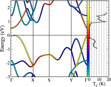
Figure 1. Left panel: Kohn–Sham LDA band structure of undoped (insulating) phosphorene. The color-scale (green to yellow) is proportional to the P-pz character of the KS-state. Right panel: estimation of the superconducting critical temperature (see text) as a function of the Fermi level position. The zero of the energy represents the valence band maximum of the undoped phosphorene.
Download figure:
Standard image High-resolution imageTo this end, we studied the EPC in one ML phosphorene and give a possible experimental way to dope the covalent  anti-bonding states, making the system metallic. The EPC and its variation with charge doping was studied as a function of the Fermi energy from negative (hole doping) to positive values (electron doping), by a rigid shifting of the Fermi energy considering the phonon frequencies calculated in the undoped (insulating) system. Although this procedure neglects renormalization of phonon frequencies induced by doping, it takes into account the modification of the Fermi surface, the variations of nesting conditions and of the EPC matrix elements. The behavior of the critical temperature as a function of doping is reported in the right panel of figure 1. A maximum Tc of the order of 15 K can be achieved moving the Fermi level at
  above the conduction band minimum. Hole doping, on the contrary, should be less promising. The estimated relevant superconducting critical temperatures upon electron doping deserves further investigations, in particular considering a more detailed and realistic system including dopant atoms.
To this end, we investigated lithium deposition as a possible route to achieve electron doping of black phosphorus' surface, or ultimately of single layer phosphorene. We simulate the black phosphorus' surface covered by Li adatoms at 1/8 of monolayer (ML) and at 1/16 of ML of concentration using respectively a 2 × 1 and 2 × 2 unit cell. Total energy calculations reveal that Li most stable adsorption site is the center of the triangle consisting of three P atoms in the surface (figure 6(a)), with a calculated binding energy of 0.18 eV. In this configuration the Fermi level shifts into the conduction band slightly modifying the pristine density of states of surface atoms (not shown). This confirms that we can consider a single phosphorene layer to calculate the phonon spectrum and EPC of Li doped system, reducing computational time still expecting quantitatively accurate predictions. We comment that some minor deviations on the calculated Tc (see below) could occur due to the fact that additional layers (or even the substrate on which a phosporene is grown) could perturb the vibrational properties of the active layer.
In addition, as a possible hole dopant, we considered carbon substitution (contrary to Li, P substitution with C is energetically favored with respect to the C adsorption on the phosphorene's surface), at a 1/7 of ML concentration. The density of states of lithium doped phosphorene is compared with the pristine and carbon doped phosphorene in figure 2, revealing that carbon can be indeed used as a possible hole dopant. Focusing on lithium, the band structure of the 1/8 doped compound (figure 3) shows that the Fermi level is shifted at 0.75 eV above the conducting band minimum at Γ: this is the region of maximum estimated Tc (see figure 1).

Figure 2. P projected density of states for clean (bold line), 1/8 of ML Li (thin line) and carbon doped (dashed line) phosphorene. The zero of the energy represents the position of the valence band maximum (Fermi level) of the undoped (doped) phosphorene.
Download figure:
Standard image High-resolution image
Figure 3. Band structure of Li-doped phosphorene at doping level of 1/8 of ML. The inset reports the surface BZ with high symmetry points. The zero of the energy represents the Fermi level.
Download figure:
Standard image High-resolution imageThe calculation of the dynamical properties reveals that Li- and C-doped systems are dynamically stable. The phonon dispersion and density of states of pure phosphorene reported in figures 4(a) and (b), respectively, are characterized by an energy gap between lower optical and higher optical branches of ≃10 meV, which is filled upon Li doping by modes which involve Li displacement, as confirmed by the projected phonon density of states in figure 4(c). At the same time, we observe a softening of the highest P–P stretching modes caused by the filling of the anti bonding  states. The calculation of the Eliashberg function,
  , for Li- and C-doped phosphorene reported in figure 5, partially confirms the estimations based on the rigid band model: at 1/8 ML (1/16 ML) of Li doping we obtain
  with an estimated superconducting critical temperature of 17 K(3 K). On the other hand, carbon dopig is strongly detrimental for the EPC, and does not induce superconductivity.
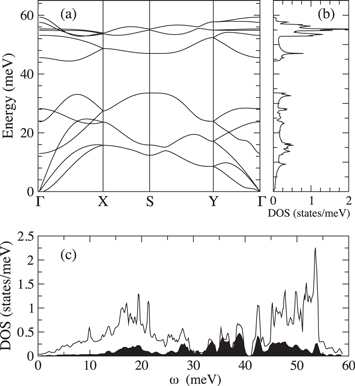
Figure 4. Phononic band structure (panel (a)) and density of states of undoped phosphorene (panel (b)). Panel (c): phonon DOS of 1/8 monolayer Li-doped phosphorene. The black shaded area highlights Li derived frequencies.
Download figure:
Standard image High-resolution image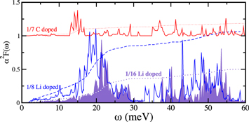
Figure 5. Eliashberg functions:  upon 1/8 of monolayer Li doping (blue full line), 1/16 of monolayer Li doping (shaded area) and 1/7 of ML carbon doping (upward shifted red line). The dotted and dashed curves represent
  leading to the total coupling
  for 1/8 of ML Li doping,
  for 1/16 of ML Li doping and
  for 1/7 of ML C doping (this curve is also shifted upward of 1 unit).
Download figure:
Standard image High-resolution image2. Experimental results
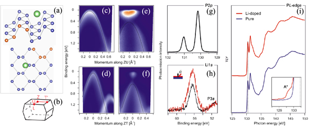
Guided by the successful theoretical results, we considered the experimental realization of lithium doped black phosphorus' surface and investigate the electronic properties in order to confirm the semiconductor-metal transition. For the experimental realization of the system we used commercially available black phosphorus crystals (99.999999%, Smart-Elements GmbH, HQ Graphene). The samples were cleaved by a scotch tape in the load-lock chamber of the beamline end station at a pressure better than 10−8 mbar. Li was evaporated [13, 24] onto the cold sample (T = 20 K) until the Fermi level position was not shifting anymore. The total amount of deposited Li corresponded to ∼1/8 of ML according to quartz microbalance and x-ray photoemission spectroscopy (XPS) data. The XPS and near edge x-ray absorption fine structure (NEXAFS) measurements were carried out at the German-Russian beamline (RGBL) [25] at the Helmholtz-Zentrum Berlin. Core level photoemission spectra were acquired at normal (90°) and grazing (30°) emission angles with respect to the sample surface. Li1s and P2p core-level spectra were acquired using  excitation energy. NEXAFS was measured in total electron yield mode at 55° incidence angle and then normalized to the intensity of incident radiation. High-resolution ARPES scans through the Z point along the ZU and
  directions were recorded at the BaDElPh beamline [26] of the Elettra synchrotron in Trieste (Italy) using linearly polarized radiation. ARPES spectra were acquired at a photon energy of 20 eV with the sample held at 20 K and a base pressure better than
  mbar. The total angular and energy resolution was determined to 0.15° and 15 meV, respectively. We performed our photoemission studies in both p- and s-polarizations. We have determined the inner potential V0 [27] by performing ARPES measurements along the
  direction with different photon energies in the range 10–40 eV. The Z point could be easily identified as the symmetry point where the valence band is closest to the Fermi level. This allowed us to find
  . This yields the Z point for a photon energy of 20 eV and is fully consistent with previous data [4]. ARPES measurements of pristine black phosphorusalong the ZU and
  line (figure 6 (b)) of the Brillouin zone (BZ) (shown in figures 6 (c) and (d), respectively) show the valence band maximum located at the Z point, revealing the semiconducting nature of the compound.
Figure 6. (a) Sketch of one-layer black phosphorus's (phosphorene) crystal structure, showing Li atom's (green atom) most stable adsorption site. Orange atoms represent the four atoms of the black phosphorus's primitive cell. (b) The Brillouin zone of black phosphorus. The ARPES spectra (referred to the chemical potential) of pristine black phosphorus recorded for (c) ZU and (d) ZT symmetry directions. ARPES spectra after Li doping along the (e) ZU and (f) ZT symmetry directions. (g) and (h) Depict the XPS spectra of the P2p and the Li1s core levels of doped black phosphorus, respectively. In panel (i), we report the x-ray absorption spectra for pristine and doped black phosphorus.
Download figure:
Standard image High-resolution image
The ARPES data along the same lines of the BZ, but after deposition ∼1/8 ML of Li are shown in figures 6(e) and (f). The Fermi level shifts into the previously unoccupied conduction band across the band gap (measured to be 340 meV) by ∼110 meV above the conduction band minimum at the Z-point. The effective valence band masses are strongly anisotropic,  (ZU direction) and
  (
( direction), and are not renormalised by lithium doping (within the experimental accuracy). These values are in satisfactory agreement with the theoretical estimations considering that the value of the tiny effective mass along y direction is strongly dependent on the computational details. Figures 6 (g) and (h) depict XPS measurements of the P2p and Li1s core levels of doped black phosphorus, respectively. As it can be seen in figure 6(h) the Li1s photoemission is more intense at grazing emission, indicating that Li atoms lie on black phosphorus'(s) surface and not intercalated into the bulk. The x-ray absorption spectrum of pristine and Li-doped black phosphorus in figure 6(i), reveals only subtle modifications upon doping. In particular, after Li doping a small shoulder appears at an energy lower than the absorption edge. Since we do not see important modifications of the ARPES and XPS we rule out defects as the source for this shoulder. Instead, we attribute this shoulder to dynamical effects in Li-doped black phosphorus'(s) surface as a result of a charge-transfer induced dipole. We conclude that the semiconductor-metal transition of black phosphorus and phosphorene can be obtained by lithium doping.
In conclusion, the theoretical predictions of sizable EPC and superconducting phase at 17 K in lithium doped black phosphorus's surface or phosphorene, and its demonstrated experimental feasibility deserves further dedicated studies, already performed on other 2D systems [28], like four-point probe electrical transport measurements [29] to confirm the existence of a superconducting phase in phosphorene.
Acknowledgments
The research leading to these results has received funding from the European Community Seventh Framework Program (FP7/2007–2013) under grant agreement n.312284 (CALIPSO). We thank HZB and Elettra for the allocation of synchrotron radiation beamtime and support during the stay. AG acknowledges the ERC grant no. 648589 SUPER-2D, funding from Quantum Matter and Materials and DFG project GR 3708-2/1. GP acknowledges support by the EU-Japan project (No. 283204 SUPER-IRON) and by the Supercomputing center Cineca (Bologna, Italy) through ISCRA projects. A.V.F and D.Yu.U acknowledge the support of Saint Petersburg State University (research Grant No. 15.61.202.2015).